A Novel HDL Coding Style to Reduce Power
Consumption for Reconfigurable Devices
Thomas Marconi, Dimitris Theodoropoulos, Koen Bertels, Georgi Gaydadjiev
Computer Engineering Lab, Delft University of Technology
{thomas,dtheodor,koen,georgi}@ce.et.tudelft.nl
Abstract—Power consumption has become the major factor that has to be considered while designing systems using recon-figurable devices, especially for battery-operated applications. Minimizing transitions is one of the ways to reduce power consumption. Overwriting a register with the same value occurs frequently in real digital systems. Such unneeded transitions increase the power consumption. To avoid this, a new HDL coding style to reduce power consumption for reconfigurable devices is proposed. The idea is to ”force” the CAD tool to configure the CLB flip-flop as a T flip-flop with its T input held constantly at logic one and drive its clock through the lookup table(LUT). Based on an extensive evaluation using MCNC benchmark circuits on a real FPGA and a real CAD tool, our proposal reduces total power consumption by 13-90 % and runs 2-20 % faster with 0-45 % area overhead compared to conventional coding style solutions. As a parallel activity we proposed a new logic element (LE) that implements the proposed design style directly.
I. INTRODUCTION
It is well known that dynamic power consumption is linearly proportional to switching activity and capacitance and has a quadratical relation to supply voltage. Therefore, one of the ways to reduce dynamic power consumption is to reduce switching activity. In real systems, many transitions are not necessary. For example, rewriting a register with the same value as its original one, is not needed. This unneeded tran-sition increases switching activity, thus consuming power for doing useless operations. Moreover, as reported in [17], even low-power flip-flops consume power during logic transition from zero-to-zero and from one-to-one.
Hardware Description Language (HDL) coding style can affect performance, area and power consumption. We observe that almost all existing coding styles focus on improving performance and reducing area. In our coding style, we focus on reducing power consumption. Another observation is that all existing styles still use what we call it as ”conventional coding style”. In conventional coding style, each flip-flop is coded into one process. This process will generate a D flip-flop (DFF) with the D input coming from the output of the corresponding next state function. Since the clock input of DFF is directly connected to the clock signal, the DFF is always clocked even when it is not necessary. For example, when the D input has the same logic value as the Q output (D = Q), the DFF does not need to be clocked. This unnecessary logic transition wastes power.
To avoid such unnecessary transitions, a new HDL coding style to reduce power consumption for reconfigurable devices
is proposed. The Microelectronic Center of North Carolina (MCNC) benchmark circuits [1] are used to evaluate the proposed coding style compared to conventional coding style. Our proposal can be used with any HDL. In this paper, we illustrate it using VHDL. Each MCNC benchmark circuit is converted into two VHDL files to represent two VHDL coding styles (conventional coding style and our proposal). The VHDL files are implemented in a real FPGA (Stratix EP1S10F484C5 from Altera) using a real existing FPGA tool (Quartus II 6.0 from Altera). The effect of the proposed VHDL coding style on power consumption, area, and performance is evaluated in comparison with conventional one.
The main contributions of this paper are:
• a novel low power coding style for reconfigurable
de-vices;
• reduction in total power consumption by 13-90 % with
0-45 % area overhead;
• performance improvement by 2-20 %.
The remainder of this paper is organized as follows. In Section II, we present related work in HDL coding styles. Our proposed coding style to reduce power is presented in Section III. In Section IV, we evaluate our HDL coding style. Finally, in Section V, we summarize the paper.
II. RELATED WORK
One of the early references about how HDL coding style affects design performance is presented in [2]. The author mainly focuses on certain VHDL constructs and how effi-ciently are interpreted by synthesis tools. A similar work is presented in [3], where a VHDL design methodology adapted to FPGA architectures is described. The authors discuss how different VHDL constructs can lead to suboptimal implementations. Furthermore, they compare different Finite State Machines (FSMs) encoding schemes when mapped onto FPGAs and ASICs.
A more recent study focusing on FSMs is presented in [4]. The conclusions were that a two-block approach for FSM designs with combinational outputs and a three-block approach for registered ones are the best strategies respectively. Another similar study on FSM coding styles for FPGAs is presented in [5]. The authors designed a FSM using three different methods, and report how area utilization is affected under each one of them.
TABLE I
RELATED WORK CATEGORIZED ACCORDING TO OPTIMIZATION GOALS
Optimization goal Reference
Performance [2], [3], [4], [5], [6], [7], [8], [10] Area [2], [3], [4], [5], [6], [7], [8], [9], [10]
Power [11], [12], [13]
respectively. Also, the authors in [8] address many important factors that can help improving the design by increasing the maximum operating frequency and/or reducing area utiliza-tion. In [9], the author describes how to reduce area utilization up to 50% by demonstrating simple HDL coding techniques. The conclusion of the paper is that following the signal priorities of flip-flops, allows the synthesis tools to optimize designs for low area utilization.
The authors in [10] describe a case study that was conducted about how HDL coding style affects design performance. Re-ported results demonstrate how an HDL behavioral approach leads to more efficient implementations compared to structural descriptions. This fact is also supported by [8], where the authors explicitly suggest to describe designs behaviorally as much as possible.
HDL coding style to reduce power consumption in a liter-ature is clock gating. Clock gating is used to reduce dynamic power consumption by selectively stop the clock signal to go to storage elements when no state or output transition takes place [11][12][13].
Almost all coding styles focus on improving performance and reducing area as shown in Table I. In our coding style, we focus on reducing power consumption. Our coding style is different from clock gating. In clock gating [11][12][13], the process to represent each flip-flop is modeled by DFF with the D input from the output of the next state function; while in our style, the flip-flop is modeled by T flip-flop (TFF) with the T input at logic one. This is related to the fact that designing sequential circuits using TFFs is more power efficient than DFFs as already reported in [16]. Moreover, there is no next state function anymore that goes to the input of T flip-flop; the input of T flip-flop is constant at logic one. To know when to stop clock signal, the clock gating needs a controller that has a knowledge of the circuit behavior. In our style, the controller has been unified with the next state function circuit.
III. PROPOSEDHDLCODING STYLE
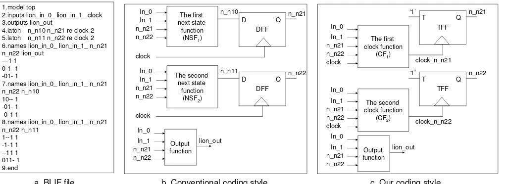
To discuss the basic idea of proposed HDL coding style, an example of MCNC benchmark circuit in Berkeley Logic Interchange Format (BLIF) [14] is presented in Figure 1a. This simple example circuit (lion.blif) has two flip-flops (lines 4 and 5) and three combinational logic functions (lines 6-8). Line 6 is the output function; while lines 7 and 8 are next state functions. In conventional coding style, each flip-flop is coded into one process. This process will generate a DFF with the D input from the output of corresponding next state function (NSF) as shown in Figure 1b. In this circuit, the output of each NSF is connected to the D input of DFF. When the D input of DFF (in this figure, for example: n n10 and n n11)
has a different value compared to its Q output (D̸=Q), the DFF needs to be clocked for updating the storage data (in this figure, for example: n n21 and n n22). Otherwise, when the D input has the same logic value as the Q output (D =Q), the DFF does not need to be clocked. However, since the clock input of DFF is directly connected to the clock signal, the DFF is always clocked. This unnecessary logic transition wastes power.
To solve this issue, we propose a new coding style as shown in Figure 1c. A more detailed report of this proposal can be found in [19]. Contrary to conventional coding style, in our approach, each flip-flop is represented into two processes. The first process is used to model a TFF with T at logic one; while the second process is used to create a function for feeding the clock input of the TFF. We call this function as a clock function (CF). The TFF is clocked when it is needed to update storage data (in this simple example: n n21 and n n22); otherwise, it will not be clocked. In this simple circuit, for example if present state of n n21 is different from next state of n n21, the TFF will be clocked by clock n n21; otherwise, it will not be clocked to save power.
Avoiding unnecessary clock transitions is one of benefits of this new coding style compared to conventional coding style. Each combinational circuit stops clock signal to be propagated to an individual FF when the state of the FF does not change. As a result, the unnecessary clock transitions are totally avoided. In comparison to clock gating, our coding style does not need an additional clock gating controller. As a result, additional power and area are also saved in comparison to clock gating approach.
Moreover, circuits generated using our proposed coding style can run faster than circuits using conventional coding style. This can be explained as follows. In conventional circuits, the DFF can be clocked properly if its D input is stable at least before its setup time (tsetup(DF F)). In our circuits, since the T input of the TFF is always connected to logic one, the TFF is always ready to be clocked. As a result, logic circuits implemented using our style can be clocked faster than logic circuits using conventional style. In order to obtain the clock period of the circuit using conventional style, equation (1) can be used:
TcConv(N)≥M ax(tpd(N SF1), tpd(N SF2), ...,
tpd(N SFN)) +tpcq(DF F) +tsetup(DF F) (1)
wheretpd is the propagation delay of combinational logic, N is the number of NSFs andtpcqis the clock-to-Q propagation delay of flip-flop. Similarly, the clock period using our coding style can be calculated using the following equation:
TcOur(M)≥M ax(tpd(CF1), tpd(CF2), ...,
tpd(CFM)) +tpcq(T F F)
(2)
Output
2.inputs lion_in_0_ lion_in_1_ clock 3.outputs lion_out
4.latch n_n10 n_n21 re clock 2 5.latch n_n11 n_n22 re clock 2 6.names lion_in_0_ lion_in_1_ n_n21 n_n22 lion_out
---1 1 0-1- 1 -01- 1
7.names lion_in_0_ lion_in_1_ n_n21 n_n22 n_n10
10-- 1 -01- 1 -0-1 1
8.names lion_in_0_ lion_in_1_ n_n21 n_n22 n_n11
a. BLIF file b. Conventional coding style c. Our coding style
Fig. 1. Basic idea and eq. (2) M=2, and obtain the speedup asSP EEDU P =
TConv c (2)
TOur c (2).
In our style, we need to feed clock signal to combinational circuits (implemented in LUTs in FPGAs) before it goes to flip-flops. This can be easily applied since not all inputs of LUTs are utilized in real FPGA designs as reported in [15]. Therefore, we can use these unused inputs to feed clock signal for free in FPGAs.
If the input of circuit changes during clock signal at logic one, there is a chance that this input generates a pulse that can affect the state of TFF. The first solution of this problem is to use the pulsed clock signal. The width of pulsed clock signal is set to be the minimum pulsed clock width of TFF. Since the width of the pulsed clock signal is so narrow, the possibility that inputs change during this very short period is kept low. If it occurs, the width of the pulse caused by this condition is always less than the width of the original pulsed clock signal. Since the width of this pulse is smaller than the minimum pulsed clock width of TFF, the pulse is ignored; the state of TFFs will not be affected. As a result, the circuit will keep working properly. The second solution for this clocking problem is to synchronize the input with clock signal before it goes to the actual circuit. Since inputs are synchronized, the changing of input during clock at logic one will be ignored by the circuit. However, this requires additional logic, latency and power. In this paper, we performed experiments using a pulsed clock solution.
IV. EVALUATION
The experimental setup is shown in Figure 2. Each MCNC benchmark circuit [1] is converted into two VHDL files (conventional and our VHDL files) to represent the two VHDL coding styles (conventional and our coding styles). Each VHDL file is compiled for Stratix EP1S10F484C5 using the Compiler Tool from Quartus II. The area needed for implementing each circuit in the number of logic elements (LEs) is reported by the Compiler Tool. Waveform Editor from
BLIF input file (MCNC benchmark circuit)
Conventional BLIF to VHDL converter
Conventional VHDL file
Compiler Tool
Implemented conventional/our circuit Conventional/Ourarea
Simulation Tool
Our BLIF to VHDL converter
Our VHDL file
Fig. 2. Experimental setup
Quartus II is used to generate test vectors for each bench-mark circuit. Those vectors are applied to the implemented circuit using Simulation Tool from Quartus II. Each circuit is verified by comparing the simulation results between the conventional and our circuits. This step is needed to ensure that both generated circuits are functionally correct with the same working functionality. Besides generating simulation results, the Simulation Tool also generates the signal activity file (SAF). To evaluate power consumption, this SAF file and the implemented circuit from the previous step are fed into the PowerPlay Power Analyzer Tool from Quartus II to obtain total power, dynamic power, and static power. To compare the performance of the implemented circuits, Timing Analyzer from Quartus II is used. The performance is obtained in terms of maximum clock frequency.
TABLE II
EXPERIMENTAL RESULTS AT50 MHZ
Dynamic power (mW) Total power (mW) Static power (mW) Area (#LEs) Maximum clock frequency(MHz)
Circuits conv our reduction conv our reduction conv our conv our overhead conv our improvement
(%) (%) (%) (%)
lion 39.87 4.75 88.09 227.37 192.25 15.45 187.5 187.5 7 7 0 437.06 467.07 6.87
bbara 36.2 0.78 97.85 223.7 188.28 15.83 187.5 187.5 25 29 16 305.44 340.02 11.32
bbsse 39.58 6.43 83.75 227.08 193.93 14.6 187.5 187.5 45 49 8.89 264.27 274.73 3.96
s298 45.81 10.54 76.99 233.31 198.04 15.12 187.5 187.5 740 903 22.03 93.82 95.27 1.55
dk16 51.82 16.93 67.33 239.32 204.43 14.58 187.5 187.5 85 86 1.18 219.97 226.3 2.88
dk14 55.58 16.32 70.64 243.08 203.82 16.15 187.5 187.5 28 37 32.14 276.78 331.79 19.87
tbk 40.47 4.3 89.37 227.97 191.8 15.87 187.5 187.5 69 78 13.04 139.14 153.82 10.55
beecount 44.92 9.56 78.72 232.42 197.06 15.21 187.5 187.5 11 16 45.45 367.92 390.63 6.17
cse 41.96 6.48 84.56 229.46 193.98 15.46 187.5 187.5 73 80 9.59 216.08 232.34 7.52
s1494 71.73 27.17 62.12 259.23 214.67 17.19 187.5 187.5 249 261 4.82 190.99 208.9 9.38
ex1 48.71 16.81 65.49 236.21 204.31 13.5 187.5 187.5 110 118 7.27 242.19 256.41 5.87
keyb 41.09 5.21 87.32 228.59 192.71 15.7 187.5 187.5 90 96 6.67 190.19 214.5 12.78
planet 42.33 5.88 86.11 229.83 193.38 15.86 187.5 187.5 215 231 7.44 188.82 210.7 11.59
pma 89.47 53.51 40.19 276.97 241.01 12.98 187.5 187.5 76 83 9.21 210.39 224.77 6.83
s1 52.95 21.23 59.91 240.45 208.73 13.19 187.5 187.5 140 146 4.29 117.04 120.44 2.9
styr 66.53 31.55 52.58 254.03 219.05 13.77 187.5 187.5 202 210 3.96 298.78 310.95 4.07
s1488 63.96 30.37 52.52 251.46 217.87 13.36 187.5 187.5 243 255 4.94 194.89 197.71 1.45
sand 36.14 0.49 98.64 223.64 187.99 15.94 187.5 187.5 205 213 3.9 180.08 199.48 10.77
dynamic power consumption (75 % on average) compared to conventional style. The degree of power reduction depends on the nature of the circuit, circuits with many unnecessary transitions can take more advantages of our style in terms of power consumption. This 75 % dynamic power reduction can only produce 15 % reduction in total power consumption on average at 50 MHz since the static power is a dominant power in these circuits at this frequency. If the dominant power is dynamic power, this 75 % reduction in dynamic power will lead to reduction in total power up to 75 %.
Our style can also increase the performance of the circuits by 7.6 % on average. This can be explained as following. Since we force CAD tools to implement each flip-flop using a TFF with the T input at logic one in our style, the flip-flop is always ready to be clocked; it does not need to wait for setup time of the flip-flop before it can be clocked. Since the setup time is becoming far less significant compared to the longest path for more logic level circuits, more logic level leads to less performance improvement.
Since clock signal needs to be fed to LUTs before it goes to flip-flops, our style suffers 0-45% (11 % on average) more area compared to the conventional one, depending on the circuit logic functions. If the clock signal can be fed to LUTs using unused inputs, our style does not need additional LUTs for this purpose. As a result, it will produce lower area overhead or even no area overhead as shown in Table II. In our experiment, we had considered this area overhead when we evaluated power consumption and performance.
To investigate all implemented circuits further, we run them using different clock frequencies: 100 MHz and 150 MHz. The results of this experiment are presented in tables III and IV. Since static power, area, and performance are not affected by changing the clock frequency, these tables only show dynamic power and total power consumptions. From these tables, we can see that dynamic power consumption is linearly proportional with clock frequency. These tables also show that our coding style can reduce total power consumptions by 25 % and 32 % on average compared to conventional style at
TABLE III
EXPERIMENTAL RESULTS AT100 MHZ
Circuits Dynamic power (mW) Total power (mW)
conv our reduction(%) conv our reduction(%)
lion 79.74 9.5 88.09 267.24 197 26.28
bbara 72.4 1.56 97.85 259.9 189.06 27.26
bbsse 79.16 12.86 83.75 266.66 200.36 24.86
dk16 103.64 33.86 67.33 291.14 221.36 23.97
dk14 111.16 32.64 70.64 298.66 220.14 26.29
tbk 80.94 8.6 89.37 268.44 196.1 26.95
beecount 89.84 19.12 78.72 277.34 206.62 25.5
cse 83.92 12.96 84.56 271.42 200.46 26.14
s1494 143.46 54.34 62.12 330.96 241.84 26.93
ex1 97.42 33.62 65.49 284.92 221.12 22.39
keyb 82.18 10.42 87.32 269.68 197.92 26.61
planet 84.66 11.76 86.11 272.16 199.26 26.79
pma 178.94 107.02 40.19 366.44 294.52 19.63
s1 105.9 42.46 59.91 293.4 229.96 21.62
styr 133.06 63.1 52.58 320.56 250.6 21.82
s1488 127.92 60.74 52.52 315.42 248.24 21.3
sand 72.28 0.98 98.64 259.78 188.48 27.45
TABLE IV
EXPERIMENTAL RESULTS AT150 MHZ
Circuits Dynamic power (mW) Total power (mW)
conv our reduction(%) conv our reduction(%)
lion 119.61 14.25 88.09 307.11 201.75 34.31
bbara 108.6 2.34 97.85 296.1 189.84 35.89
bbsse 118.74 19.29 83.75 306.24 206.79 32.47
dk16 155.46 50.79 67.33 342.96 238.29 30.52
dk14 166.74 48.96 70.64 354.24 236.46 33.25
beecount 134.76 28.68 78.72 322.26 216.18 32.92
cse 125.88 19.44 84.56 313.38 206.94 33.97
s1494 215.19 81.51 62.12 402.69 269.01 33.2
ex1 146.13 50.43 65.49 333.63 237.93 28.68
keyb 123.27 15.63 87.32 310.77 203.13 34.64
planet 126.99 17.64 86.11 314.49 205.14 34.77
pma 268.41 160.53 40.19 455.91 348.03 23.66
styr 199.59 94.65 52.58 387.09 282.15 27.11
s1488 191.88 91.11 52.52 379.38 278.61 26.56
sand 108.42 1.47 98.64 295.92 188.97 36.14
100 MHz and 150 Mhz, respectively. Since dynamic power is higher when the clock frequency is increased, the reduction of total power is also increased for higher clock frequency.
0 10 20 30 40 50 60 70 80 90 100
0 1 2 3 4 5 6 7 8 9 10 11
#Circuits
T
o
ta
l
p
o
w
e
r
re
d
u
c
ti
o
n
(
%
)
50 MHz
100 MHz
150 MHz
200 MHz
250 MHz
300 MHz
Fig. 3. Effect of the number of circuits (#Circuits) on total power reduction (%) at different clock frequencies
TABLE V
COMPARISON WITH CLOCK GATING SOLUTIONS
Evaluation Our solution Clock Gating solutions
[11] [12] [13]
Power 13-90% 6.2-7.7% 5-33% 1.8-27.9%
lower lower lower lower
Performance 2-20% faster 0-2% slower Not available 1.1% faster Area 0-45 % overhead Not available Not available Not available
dynamic power; the dynamic power becomes more dominant compared to static power. Since our style can only reduce dynamic power, it can save more dynamic power for more working circuits. As a result, our style reduces much more total power when the number of circuits inside the FPGA increases. This figure indicates that our style can reduce total power by 16-65 % at 50 MHz. Total power is even much more reduced at higher frequency, up to 90 % at 300 MHz. Total power reduction saturates up to its ability to reduce dynamic power. Table V shows the comparison between our solution and clock gating solutions [11], [12], and [13]. Clock gating solutions are obtained from the results of the original papers: [11], [12], and [13]. Unlike clock gating, our proposal does not need an additional controller to stop clock propagation. As a result, it saves more power than clock gating solutions. Moreover, since flip-flops are always ready to be clocked in our proposal, it generates faster designs than clock gating designs. The area cannot be directly compared due to no information regarding area overhead in clock gating papers.
V. CONCLUSIONS
In this paper, we have proposed a novel HDL coding style to reduce power consumption of designs targeting reconfigurable devices. The proposed style has been evaluated using MCNC benchmark circuits on a real FPGA and a real CAD tool. By avoiding unnecessary transitions, the proposed style produces circuits with 13-90 % less total power consumption compared to conventional style. Moreover, by making ”always ready” flip-flops, the circuits generated from our style run 2-20 % faster than the conventional one. Since the proposed style needs to feed clock signal to its combinational logic, the
proposed style creates circuits with 0-45 % more area. This result motivated new proposal for a low power LE to support this way of implementing circuits as reported in [18]. Instead of using DFFs, we use TFFs with the T input permanently connected to logic one value. Instead of connecting the output of the LUT to the input of the FF, we connect it to the clock input of the FF. The coding style in this paper is a way for us to ”force” the existing CAD tools using the existing FPGAs to implement circuits in a different way than the conventional one. In the future, this new way of implementing circuits could be integrated in the CAD tools.
ACKNOWLEDGMENT
This work is sponsored by the hArtes project (IST-035143) supported by the Sixth Framework Programme of the Euro-pean Community under the thematic area ”Embedded
Sys-tems”. REFERENCES
[1] S. Yang, Logic Synthesis and Optimization Benchmarks User Guide Version 3.0, Tech. Rep., Microelectronic Center of North Carolina, 1991. [2] S. Samhouri, HDL Coding Style for LUT Based FPGAs, Proceedings of IEEE International Verilog HDL Conference and VHDL International Users Forum, pp. 1-11, 1996.
[3] M. Gschwind and V. Salapura, A VHDL design methodology for FPGAs, Proceedings of International Conference on Field Programmable Logic and Applications(FPL), pp. 208-217, 1995.
[4] C. E. Cummings, The Fundamentals of Efficient Synthesizable Finite State Machine Design using NC-Verilog and BuildGates, Proceedings of International Cadence Usergroup Conference, pp. 1-27, 2002. [5] N. I. Rafla and B. L. Davisy, A Study of Finite State Machine Coding
Styles for Implementation in FPGAs, Proceedings of International Midwest Symposium on Circuits and Systems, pp. 337-341, 2006. [6] Coding Style Guidelines, Xilinx, Tech. Rep., 2003.
[7] Quartus II Handbook Version 9.1, Altera, Tech. Rep., November 2009. [8] P. Garrault and B. Phiofsky, HDL Coding Practices to Accelerate Design
Performance, Xilinx Corporation , Tech. Rep., January 2006. [9] K. Chapman, Get your Priorities Right Make your design up to 50%
smaller, Xilinx Corporation, Tech. Rep., October 2007.
[10] A. Dollas, K. Papademetriou, E. Sotiriades, D. Theodoropoulos, I. Koidis, and G. Vernardos, A Case Study on Rapid Prototyping of Hardware Systems: the Effect of CAD Tool Capabilities, Design Flows, and Design Styles, Proceedings of IEEE International Workshop on Rapid System Prototyping, pp. 180-186, June 2004.
[11] S. Huda, M. Mallick, J.H. Anderson, Clock gating architectures for FPGA power reduction, Proceedings of International Conference on Field-Programmable Logic and Applications(FPL), pp. 112-118, 2009. [12] Y. Zhang, J. Roivainen, A. M¨ammel¨a, Clock-Gating in FPGAs: A Novel and Comparative Evaluation, Proceedings of EUROMICRO Conference on Digital System Design, pp.584-590, 2006
[13] Q. Wang, S. Gupta, J.H. Anderson, Clock power reduction for Virtex-5 FPGAs, Proceedings of International Conference on Field Programmable Gate Arrays (FPGA), pp. 13-22, 2009.
[14] Berkeley Logic Interchange Format (BLIF), University of California Berkeley, February 2005.
[15] S. Mondal and S. O. Memik, Fine-grain leakage optimization in SRAM based FPGAs, Proceedings of the ACM Great Lakes Symposium on VLSI, pp. 238-243, 2005.
[16] X. Wu, M. Pedram, Low-power Sequential Circuit Design Using T Flip-flops, International Journal of Electronics, Vol. 88, No. 6, pp. 635-643, June 2001.
[17] D. Markovic, B. Nikolic, R. Brodersen, Analysis and design of low-energy flip-flops, Proceedings of International Symposium on Low Power Electronics and Design, pp.52-55, August 2001.
[18] T. Marconi, K. Bertels, G. Gaydadjiev, A Novel Logic Element for Power Reduction in FPDs, CE-TR-2010-01, Computer Engineering Lab, TU Delft, January 2010.