1
❘❙❚❘❙❚❘❙❚❘❙❚❘❙❚❘❙❚❘❙❚❘❙❚❘❙❚❘❙❚❘❙❚
❙❚❘❙❚❘❙❚❘❙❚❘❙❚❘❙❚❘❙❚❘❙❚❘❙❚❘❙❚❘❙❚❘❙❚❘❙❚❘❙❚❘❙❚❘❙❚❘❙❚❘❙❚❘❙❚❘❙❚❘❙❚❘❙❚❘❙❚❘❙❚❘❙❚❘❙❚❘❙❚❘❙❚❘❙❚❘❙❚❘❙❚❘❙❚❘❙❚❘❙❚❘❙❚❘❙❚❘❙❚❘❙❚❘❙❚❘❙❚❘❙❚❘❙❚❘❙❚❘❙❚❘❙❚❘❙❚❘❙❚❘❙❚❘❙❚❘❙❚❘❙❚❘❙❚❘❙❚❘❙❚❘❙❚❘❙❚❘❙❚❘❙❚❘❙❚❘❙❚❘❙❚❘❙❚❘❙❚❘❙❚❘❙❚
C H A P T E R
1
Basic Principles of Digital
Systems
O U T L I N E 1.1 Digital Versus
Analog Electronics 1.2 Digital Logic Levels 1.3 The Binary Number
System 1.4 Hexadecimal
Numbers
1.5 Digital Waveforms
C H A P T E R O B J E C T I V E S
Upon successful completion of this chapter, you will be able to: • Describe some differences between analog and digital electronics. • Understand the concept of HIGH and LOW logic levels.
• Explain the basic principles of a positional notation number system. • Translate logic HIGHs and LOWs into binary numbers.
• Count in binary, decimal, or hexadecimal.
• Convert a number in binary, decimal, or hexadecimal to any of the other number bases.
• Calculate the fractional binary equivalent of any decimal number.
• Distinguish between the most significant bit and least significant bit of a bi-nary number.
• Describe the difference between periodic, aperiodic, and pulse waveforms. • Calculate the frequency, period, and duty cycle of a periodic digital
wave-form.
• Calculate the pulse width, rise time, and fall time of a digital pulse.
D
igital electronics is the branch of electronics based on the combination and switching of voltages called logic levels. Any quantity in the outside world, such as temperature, pressure, or voltage, can be symbolized in a digital circuit by a group of logic voltages that, taken together, represent a binary number. ■Each logic level corresponds to a digit in the binary (base 2) number system. The b i-nary digits, or bits, 0 and 1, are sufficient to write any number, given enough places. The hexadecimal (base 16) number system is also important in digital systems. Since every combination of four binary digits can be uniquely represented as a hexadecimal digit, this system is often used as a compact way of writing binary information.
Inputs and outputs in digital circuits are not always static. Often they vary with time. Time-varying digital waveforms can have three forms:
1. Periodic waveforms, which repeat a pattern of logic 1s and 0s 2. Aperiodic waveforms, which do not repeat
1.1
Digital Versus Analog Electronics
Continuous Smoothly connected. An unbroken series of consecutive values with no instantaneous changes.
Discrete Separated into distinct segments or pieces. A series of discontinuous values.
Analog A way of representing some physical quantity, such as temperature or ve-locity, by a proportional continuous voltage or current. An analog voltage or current can have any value within a defined range.
Digital A way of representing a physical quantity by a series of binary numbers. A digital representation can have only specific discrete values.
The study of electronics often is divided into two basic areas:analogand digital electron-ics. Analog electronics has a longer history and can be regarded as the “classical” branch of electronics. Digital electronics, although newer, has achieved greater prominence through the advent of the computer age. The modern revolution in microcomputer chips, as part of everything from personal computers to cars and coffee makers, is founded almost entirely on digital electronics.
The main difference between analog and digital electronics can be stated simply. Ana-log voltages or currents are continuouslyvariable between defined values, and digital volt-ages or currents can vary only by distinct, or discrete,steps.
Some keywords highlight the differences between digital and analog electronics:
Analog Digital
Continuously variable Discrete steps Amplification Switching
Voltages Numbers
An example often used to illustrate the difference between analog and digital devices is the comparison between a light dimmer and a light switch. A light dimmer is an analog device, since it can make the light it controls vary in brightness anywhere within a defined range of values. The light can be fully on, fully off, or at some brightness level in between. A light switch is a digital device, since it can turn the light on or off, but there is no value in between those two states.
The light switch/light dimmer analogy, although easy to understand, does not show any particular advantage to the digital device. If anything, it makes the digital device seem limited.
One modern application in which a digital device is clearly superior to an analog one is digital audio reproduction. Compact disc players have achieved their high level of popu-larity because of the accurate and noise-free way in which they reproduce recorded music. This high quality of sound is possible because the music is stored, not as a magnetic copy of the sound vibrations, as in analog tapes, but as a series of numbers that represent ampli-tude steps in the sound waves.
Figure 1.1 shows a sound waveform and its representation in both analog and digital forms.
The analog voltage, shown in Figure 1.1b, is a copy of the original waveform and in-troduces distortion both in the storage and playback processes. (Think of how a photocopy deteriorates in quality if you make a copy of a copy, then a copy of the new copy, and so on. It doesn’t take long before you can’t read the fine print.)
A digital audio system doesn’t make a copy of the waveform, but rather stores a code (a series of amplitude numbers) that tells the compact disc player how to re-create the orig-inal sound every time a disc is played. During the recording process, the sound waveform
is “sampled” at precise intervals. The recording transforms each sample into a digital num-ber corresponding to the amplitude of the sound at that point.
The “samples” (the voltages represented by the vertical bars) of the digitized audio waveform shown in Figure 1.1c are much more widely spaced than they would be in a real digital audio system. They are shown this way to give the general idea of a digitized wave-form. In real digital audio systems, each amplitude value can be indicated by a number having as many as 16,000 to 65,000 possible values. Such a large number of possible val-ues means the voltage difference between any two consecutive digital numbers is very small. The numbers can thus correspond extremely closely to the actual amplitude of the sound waveform. If the spacing between the samples is made small enough, the repro-duced waveform is almost exactly the same as the original.
❘❙❚ SECTION 1.1 REVIEW PROBLEM
1.1 What is the basic difference between analog and digital audio reproduction?
1.2
Digital Logic Levels
Logic level A voltage level that represents a defined digital state in an electronic circuit.
Logic HIGH (or logic 1) The higher of two voltages in a digital system with two logic levels.
Logic LOW (or logic 0) The lower of two voltages in a digital system with two logic levels.
Positive logic A system in which logic LOW represents binary digit 0 and logic HIGH represents binary digit 1.
Negative logic A system in which logic LOW represents binary digit 1 and logic HIGH represents binary digit 0.
Digitally represented quantities, such as the amplitude of an audio waveform, are usually represented by binary, or base 2, numbers. When we want to describe a digital quantity electronically, we need to have a system that uses voltages or currents to symbolize binary numbers.
The binary number system has only two digits, 0 and 1. Each of these digits can be de-noted by a different voltage called a logic level.For a system having two logic levels, the
K E Y T E R M S FIGURE 1.1
lower voltage (usually 0 volts) is called a logic LOWor logic 0and represents the digit 0. The higher voltage (traditionally 5 V, but in some systems a specific value such as 1.8 V, 2.5 V or 3.3 V) is called a logic HIGH or logic 1,which symbolizes the digit 1. Except for some allowable tolerance, as shown in Figure 1.2, the range of voltages between HIGH and LOW logic levels is undefined.
FIGURE 1.2
Logic Levels Based on 5 V and 0 V
5 V
2 V
Logic HIGH
Logic LOW Undefined
0.8 V 0 V
For the voltages in Figure 1.2:
5 V Logic HIGH 1 0 V Logic LOW 0
The system assigning the digit 1 to a logic HIGH and digit 0 to logic LOW is called
positive logic.Throughout the remainder of this text, logic levels will be referred to as HIGH/LOW or 1/0 interchangeably.
(A complementary system, called negative logic,also exists that makes the assign-ment the other way around.)
1.3
The Binary Number System
Binary number system A number system used extensively in digital systems, based on the number 2. It uses two digits, 0 and 1, to write any number.
Positional notation A system of writing numbers where the value of a digit depends not only on the digit, but also on its placement within a number.
Bit Binary digit. A 0 or a 1.
Positional Notation
The binary number systemis based on the number 2. This means that we can write any number using only two binary digits (or bits), 0 and 1. Compare this to the decimal system, which is based on the number 10, where we can write any number with only ten decimal digits, 0 to 9.
The binary and decimal systems are both positional notationsystems; the value of a digit in either system depends on its placement within a number. In the decimal number 845, the digit 4 really means 40, whereas in the number 9426, the digit 4 really means 400 (845 800 40 5; 9426 9000 400 20 6). The value of the digit is determined by whatthe digit is as well as where it is.
In the decimal system, a digit in the position immediately to the left of the decimal point is multiplied by 1 (100). A digit two positions to the left of the decimal point is
tiplied by 10 (101). A digit in the next position left is multiplied by 100 (102). The posi-tional multipliers, as you move left from the decimal point, are ascending powers of 10.
The same idea applies in the binary system, except that the positional multipliers are powers of 2 (201, 212, 224, 238, 2416, 2532, . . .). For example, the bi-nary number 101 has the decimal equivalent:
(1 22) (0 21) (1 20) (1 4) (0 2) (1 1)
4 0 1
5
❘❙❚ EXAMPLE 1.1 Calculate the decimal equivalents of the binary numbers 1010, 111, and 10010.
SOLUTIONS 1010 (123
) (022) (121) (020) (18) (04) (12) (01) 8 2 10
111 (122) (121) (120) (14) (12) (11) 4 2 1 7
10010 (124) (023) (022) (121) (020) (116) (08) (04) (12) (01) 16 2 18
❘❙❚
Binary Inputs
Most significant bit The leftmost bit in a binary number. This bit has the number’s largest positional multiplier.
Least significant bit The rightmost bit of a binary number. This bit has the number’s smallest positional multiplier.
A major class of digital circuits, called combinational logic, operates by accepting logic levels at one or more input terminals and producing a logic level at an output. In the analy-sis and design of such circuits, it is frequently necessary to find the output logic level of a circuit for all possible combinations of input logic levels.
The digital circuit in the black box in Figure 1.3 has three inputs. Each input can have two possible states, LOW or HIGH, which can be represented by positive logic as 0 or 1. The number of possible input combinations is 238. (In general, a circuit with nbinary inputs has 2ninput combinations, ranging from 0 to 2n1.) Table 1.1 shows a list of these combinations, both as logic levels and binary numbers, and their decimal equivalents.
K E Y T E R M S
FIGURE 1.3
A list of output logic levels corresponding to all possible input combinations, applied in ascending binary order, is called a truth table. This is a standard form for showing the function of a digital circuit.
The input bits on each line of Table 1.1 can be read from left to right as a series of 3-bit binary numbers. The numerical values of these eight input combinations range from 0 to 7 (2npossible input combinations, having decimal equivalents ranging from 0 to 2n1) in decimal.
Bit Ais called the most significant bit(MSB), and bit Cis called the least significant bit (LSB). As these terms imply, a change in bit A is more significant, since it has the greatest effect on the number of which it is part.
Table 1.2 shows the effect of changing each of these bits in a 3-bit binary number and compares the changed number to the original by showing the difference in magnitude. A change in the MSB of any 3-bit number results in a difference of 4. A change in the LSB of any binary number results in a difference of 1. (Try it with a few different numbers.)
TABLE 1.1 Possible Input Combinations for a 3-Input Digital Circuit
Logic Level Binary Value Decimal Equivalent
A B C A B C
L L L 0 0 0 0
L L H 0 0 1 1
L H L 0 1 0 2
L H H 0 1 1 3
H L L 1 0 0 4
H L H 1 0 1 5
H H L 1 1 0 6
H H H 1 1 1 7
TABLE 1.2 Effect of Changing the LSB and MSB of a Binary Number
A B C Decimal
Original 0 1 1 3
Change MSB 1 1 1 7 Difference 4
Change LSB 0 1 0 2 Difference 1
FIGURE 1.4
Example 1.2: 4-Input Digital Circuit
Digital circuit
A (MSB)
D (LSB) B
Y C
Inputs Outputs
❘❙❚
Knowing how to construct a binary sequence is a very important skill when working with digital logic systems. Two ways to do this are:
1. Learn to count in binary. You should know all the binary numbers from 0000 to 1111 and their decimal equivalents (0 to 15). Make this your first goal in learning the basics of digital systems.
Each binary number is a unique representation of its decimal equivalent. You can work out the decimal value of a binary number by adding the weighted values of all the bits.
For instance, the binary equivalent of the decimal sequence 0, 1, 2, 3 can be written using two bits: the 1’s bit and the 2’s bit. The binary count sequence is:
00 (0 0) 01 (0 1) 10 (2 0) 11 (2 1)
To count beyond this, you need another bit: the 4’s bit. The decimal sequence 4, 5, 6, 7 has the binary equivalents:
100 (4 0 0) 101 (4 0 1) 110 (4 2 0) 111 (4 2 1)
The two least significant bits of this sequence are the same as the bits in the 0 to 3 sequence; a repeating pattern has been generated.
SOLUTION Since there are four inputs, there will be 24
16 possible input combina-tions, ranging from 0000 to 1111 (0 to 15 in decimal). Table 1.3 shows the list of all possi-ble input combinations.
The MSB has a value of 8 (decimal).
TABLE 1.3 Possible Input
Combinations for a 4-Input Digital Circuit
A B C D Decimal
0 0 0 0 0
0 0 0 1 1
0 0 1 0 2
0 0 1 1 3
0 1 0 0 4
0 1 0 1 5
0 1 1 0 6
0 1 1 1 7
1 0 0 0 8
1 0 0 1 9
1 0 1 0 10
1 0 1 1 11
1 1 0 0 12
1 1 0 1 13
1 1 1 0 14
The sequence from 8 to 15 requires yet another bit: the 8’s bit. The three LSBs of this sequence repeat the 0 to 7 sequence. The binary equivalents of 8 to 15 are:
1000 (8 0 0 0) 1001 (8 0 0 1) 1010 (8 0 2 0) 1011 (8 0 2 1) 1100 (8 4 0 0) 1101 (8 4 0 1) 1110 (8 4 2 0) 1111 (8 4 2 1)
Practice writing out the binary sequence until it becomes familiar. In the 0 to 15 se-quence, it is standard practice to write each number as a 4-bit value, as in Example 1.2, so that all numbers have the same number of bits. Numbers up to 7 have leading zeros to pad them out to 4 bits.
This convention has developed because each bit has a physical location in a digital circuit; we know a particular bit is logic 0 because we can measure 0 V at a particular point in a circuit. A bit with a value of 0 doesn’t go away just because there is not a 1 at a more significant location.
While you are still learning to count in binary, you can use a second method. 2. Follow a simple repetitive pattern.Look at Tables 1.1 and 1.3 again. Notice that the least
significant bit follows a pattern. The bits alternate with every line, producing the pattern 0, 1, 0, 1, . . . . The 2’s bit alternates every two lines: 0, 0, 1, 1, 0, 0, 1, 1, . . . . The 4’s bit alternates every four lines: 0, 0, 0, 0, 1, 1, 1, 1, . . . . This pattern can be expanded to cover any number of bits, with the number of lines between alternations doubling with each bit to the left.
Decimal-to-Binary Conversion
There are two methods commonly used to convert decimal numbers to binary: sum of pow-ers of 2 and repeated division by 2.
Sum of Powers of 2
You can convert a decimal number to binary by adding up powers of 2 by inspection, adding bits as you need them to fill up the total value of the number. For example, convert 5710to binary.
641057103210
• We see that 32 (25) is the largest power of two that is smaller than 57. Set the 32’s bit to 1 and subtract 32 from the original number, as shown below.
57 32 25
• The largest power of two that is less than 25 is 16. Set the 16’s bit to 1 and subtract 16 from the accumulated total.
25 16 9
• 8 is the largest power of two that is less than 9. Set the 8’s bit to 1 and subtract 8 from the total.
• 1 is left over. Set the 1’s bit to 1 and subtract 1. 1 1 0
• Conversion is complete when there is nothing left to subtract. Any remaining bits should be set to 0.
1
32 16 8 4 2 1
57 – 32 = 25
❘❙❚ EXAMPLE 1.3 Convert 9210to binary using the sum-of-powers-of-2 method.
SOLUTION 128 92 64
1
32 16 8 4 2 1
92 – 64 = 28 64
1
32 16 8 4 2 1
92 – (64 + 16) = 12 64
0 1
1
32 16 8 4 2 1
57 – (32 + 16 + 8) = 1
1 1
1
32 16 8 4 2 1
57 – (32 + 16 + 8 + 1) = 0
1 1 0 0 1
5710 = 1110012
1
32 16 8 4 2 1
92 – (64 + 16 + 8) = 4 64
0 1 1
1
32 16 8 4 2 1
92 – (64 + 16 + 8 + 4) = 0 64
0 1 1 1 0 0
1
32 16 8 4 2 1
57 – (32 + 16) = 9 1
9210= 10111002
❘❙❚
Repeated Division by 2
Any decimal number divided by 2 will leave a remainder of 0 or 1. Repeated division by 2 will leave a string of 0s and 1s that become the binary equivalent of the decimal number. Let us use this method to convert 4610to binary.
1. Divide the decimal number by 2 and note the remainder. 46/2 23 remainder 0 (LSB)
The remainder is the least significant bit of the binary equivalent of 46.
2. Divide the quotient from the previous division and note the remainder. The remainder is the second LSB.
3. Continue this process until the quotientis 0. The last remainder is the most significant bit of the binary number.
11/2 5 remainder 1 5/2 2remainder 1 2/2 1remainder 0
1/2 0 remainder 1 (MSB)
To write the binary equivalent of the decimal number, read the remainders from the bot-tom up.
46101011102
❘❙❚ EXAMPLE 1.4 Use repeated division by 2 to convert 11510to a binary number.
SOLUTION 115/2 57 remainder 1 (LSB)
57/2 28 remainder 1 28/2 14 remainder 0 14/2 7 remainder 0 7/2 3 remainder 1 3/2 1 remainder 1 1/2 0 remainder 1 (MSB) Read the remainders from bottom to top: 1110011.
1151011100112
❘❙❚
In any decimal-to-binary conversion, the number of bits in the binary number is the exponent of the smallest power of 2 that is larger than the decimal number.
For example, for the numbers 9210and 4610,
27128 92 7 bits: 1011100 26 64 46 6 bits: 101110
Fractional Binary Numbers
Radix point The generalized form of a decimal point. In any positional number system, the radix point marks the dividing line between positional multipliers that are positive and negative powers of the system’s number base.
Binary point A period (“.”) that marks the dividing line between positional mul-tipliers that are positive and negative powers of 2 (e.g., first multiplier right of bi-nary point 21
; first multiplier left of binary point 20).
In the decimal system, fractional numbers use the same digits as whole numbers, but the digits are written to the right of the decimal point. The multipliers for these digits are neg-ative powers of 10—101(1/10), 102(1/100), 103(1/1000), and so on.
So it is in the binary system. Digits 0 and 1 are used to write fractional binary num-bers, but the digits are to the right of the binary point—the binary equivalent of the deci-mal point. (The decideci-mal point and binary point are special cases of the radix point,the general name for any such point in any number system.)
Each digit is multiplied by a positional factor that is a negative power of 2. The first four multipliers on either side of the binary point are:
binary point
23 22 21 20 21 22 23 24
8 4 2 1 1/2 1/4 1/8 1/16
❘❙❚ EXAMPLE 1.5 Write the binary fraction 0.101101 as a decimal fraction.
SOLUTION 1 1/2 1/2
0 1/4 0 1 1/8 1/8 1 1/16 1/16 0 1/32 0 1 1/64 1/64
1/2 1/8 1/16 1/64 32/64 8/64 4/64 1/64 45/64
0.70312510
❘❙❚
Fractional-Decimal-to-Fractional-Binary Conversion
Simple decimal fractions such as 0.5, 0.25, and 0.375 can be converted to binary fractions by a sum-of-powers method. The above decimal numbers can also be written 0.5 1/2, 0.25 1/4, and 0.375 3/8 1/4 1/8. These numbers can all be represented by nega-tive powers of 2. Thus, in binary,
0.510 0.12 0.2510 0.012 0.375100.0112
The conversion process becomes more complicated if we try to convert decimal frac-tions that cannot be broken into powers of 2. For example, the number 1/5 0.210cannot be exactly represented by a sum of negative powers of 2. (Try it.) For this type of number, we must use the method of repeated multiplication by 2.
Method:
1. Multiply the decimal fraction by 2 and note the integer part. The integer part is either 0 or 1 for any number between 0 and 0.999. . . . The integer part of the product is the first digit to the left of the binary point.
0.2 2 0.4 Integer part: 0
2. Discard the integer part of the previous product. Multiply the fractional part of the pre-vious product by 2. Repeat step 1 until the fraction repeats or terminates.
Read the above integer parts from top to bottom to obtain the fractional binary num-ber. Thus, 0.2100.00110011 . . .2 0.00112. The bar shows the portion of the digits that repeats.
❘❙❚ EXAMPLE 1.6 Convert 0.9510to its binary equivalent.
SOLUTION 0.95 21.90 Integer part: 1
0.90 2 1.80 Integer part: 1 0.80 2 1.60 Integer part: 1 0.60 2 1.20 Integer part: 1 0.20 2 0.40 Integer part: 0 0.40 2 0.80 Integer part: 0
0.80 2 1.60 Fraction repeats last four digits 0.95100.1111002
❘❙❚
❘❙❚ SECTION 1.3 REVIEW PROBLEMS
1.2. How many different binary numbers can be written with 6 bits? 1.3. How many can be written with 7 bits?
1.4. Write the sequence of 7-bit numbers from 1010000 to 1010111. 1.5. Write the decimal equivalents of the numbers written for Problem 1.4.
1.4
Hexadecimal Numbers
After binary numbers, hexadecimal (base 16) numbers are the most important numbers in digital applications. Hexadecimal, or hex, numbers are primarily used as a shorthand form of binary notation. Since 16 is a power of 2 (2416), each hexadecimal digit can be con-verted directly to four binary digits. Hex numbers can pack more digital information into fewer digits.
Hex numbers have become particularly popular with the advent of small computers, which use binary data having 8, 16, or 32 bits. Such data can be represented by 2, 4, or 8 hexadecimal digits, respectively.
Counting in Hexadecimal
The positional multipliers in the hex system are powers of sixteen: 1601, 16116, 162256, 1634096, and so on.
We need 16 digits to write hex numbers; the decimal digits 0 through 9 are not suffi-cient. The usual convention is to use the capital letters A through F, each letter representing a number from 1010through 1510. Table 1.4 shows how hexadecimal digits relate to their decimal and binary equivalents.
Counting Rules for Hexadecimal Numbers:
1. Count in sequence from 0 to F in the least significant digit. 2. Add 1 to the next digit to the left and start over.
3. Repeat in all other columns.
For instance, the hex numbers between 19 and 22 are 19, 1A, 1B, 1C, 1D, 1E, 1F, 20, 21, 22. (The decimal equivalents of these numbers are 2510through 3410.)
N O T E
❘❙❚ EXAMPLE 1.7 What is the next hexadecimal number after 999? After 99F? After 9FF? After FFF?
SOLUTION The hexadecimal number after 999 is 99A. The number after 99F is 9A0.
The number after 9FF is A00. The number after FFF is 1000.
❘❙❚ EXAMPLE 1.8 List the hexadecimal digits from 19016to 20016, inclusive.
SOLUTION The numbers follow the counting rules: Use all the digits in one position,
add 1 to the digit one position left, and start over.
For brevity, we will list only a few of the numbers in the sequence: 190, 191, 192, . . . , 199, 19A, 19B, 19C, 19D, 19E, 19F,
1A0, 1A1, 1A2, . . . , 1A9, 1AA, 1AB, 1AC, 1AD, 1AE, 1AF, 1B0, 1B1, 1B2, . . . , 1B9, 1BA, 1BB, 1BC, 1BD, 1BE, 1BF,
1C0, . . . , 1CF, 1D0, . . . , 1DF, 1E0, . . . , 1EF, 1F0, . . . , 1FF, 200
❘❙❚
❘❙❚ SECTION 1.4A REVIEW PROBLEMS
1.6. List the hexadecimal numbers from FA9 to FB0, inclusive. 1.7. List the hexadecimal numbers from 1F9 to 200, inclusive.
Hexadecimal-to-Decimal Conversion
To convert a number from hex to decimal, multiply each digit by its power-of-16 positional multiplier and add the products. In the following examples, hexadecimal numbers are indi-cated by a final “H” (e.g., 1F7H), rather than a “16” subscript.
❘❙❚ EXAMPLE 1.9 Convert 7C6H to decimal.
SOLUTION 7 162 71025610179210
C 1611210 1610 19210 6 160 610 110 610 199010
❘❙❚ EXAMPLE 1.10 Convert 1FD5H to decimal.
SOLUTION 1163
110409610409610 F 1621510 25610 384010 D 1611310 1610 20810 5 160 510 110 510 814910
❘❙❚
❘❙❚ SECTION 1.4B REVIEW PROBLEM
1.8 Convert the hexadecimal number A30F to its decimal equivalent.
Decimal-to-Hexadecimal Conversion
remembering to convert decimal numbers 10 through 15 into the equivalent hex digits, A through F.
Sum of Weighted Hexadecimal Digits
This method is useful for simple conversions (about three digits). For example, the decimal number 35 is easily converted to the hex value 23.
35103210310(2 16) (3 1) 23H
❘❙❚ EXAMPLE 1.11 Convert 17510to hexadecimal.
SOLUTION 25610175101610
Since 256 162, the hexadecimal number will have two digits. (11 16) 175 (10 16)
16 1
175 (A 16) 175 160 15 16 1
175 ((A 16) (F 1)) 175 (160 15) 0
❘❙❚
Repeated Division by 16
Repeated division by 16 is a systematic decimal-to-hexadecimal conversion method that is not limited by the size of the number to be converted.
It is similar to the repeated-division-by-2 method used to convert decimal numbers to binary. Divide the decimal number by 16 and note the remainder, making sure to express it as a hex digit. Repeat the process until the quotient is zero. The last remainder is the most significant digit of the hex number.
❘❙❚ EXAMPLE 1.12 Convert 3158110to hexadecimal.
SOLUTION 31581/16 1973 remainder 13 (D) (LSD)
1973/16 123remainder 5 123/16 7remainder 11 (B) 7/16 0remainder 7 (MSD)
31581107B5DH
❘❙❚
❘❙❚ SECTION 1.4C REVIEW PROBLEM
1.9 Convert the decimal number 8137 to its hexadecimal equivalent.
Conversions Between Hexadecimal and Binary
Table 1.4 shows all 16 hexadecimal digits and their decimal and binary equivalents. Note that for every possible 4-bit binary number, there is a hexadecimal equivalent.
Binary-to-hex and hex-to-binary conversions simply consist of making a conversion between each hex digit and its binary equivalent.
A
❘❙❚ EXAMPLE 1.13 Convert 7EF8H to its binary equivalent.
SOLUTION Convert each digit individually to its equivalent value:
7H 01112 EH 11102 FH 11112 8H 10002
The binary number is all the above binary numbers in sequence: 7EF8H 1111110111110002
The leading zero (the MSB of 0111) has been left out.
❘❙❚
❘❙❚ SECTION 1.4D REVIEW PROBLEMS
1.10 Convert the hexadecimal number 934B to binary.
1.11 Convert the binary number 11001000001101001001 to hexadecimal.
1.5
Digital Waveforms
Digital waveform A series of logic 1s and 0s plotted as a function of time.
The inputs and outputs of digital circuits often are not fixed logic levels but digital wave-forms,where the input and output logic levels vary with time. There are three possible types of digital waveform. Periodic waveforms repeat the same pattern of logic levels over a specified period of time. Aperiodic waveforms do not repeat. Pulsewaveforms follow a HIGH-LOW-HIGH or LOW-HIGH-LOW pattern and may be periodic or aperiodic.
Periodic Waveforms
Periodic waveform A time-varying sequence of logic HIGHs and LOWs that re-peats over a specified period of time.
Period (T) Time required for a periodic waveform to repeat. Unit: seconds (s).
Frequency (f ) Number of times per second that a periodic waveform repeats. f 1/TUnit: Hertz (Hz).
Time HIGH (th) Time during one period that a waveform is in the HIGH state.
Unit: seconds (s).
Time LOW (tl) Time during one period that a waveform is in the LOW state.
Unit: seconds (s).
Duty cycle (DC) Fraction of the total period that a digital waveform is in the HIGH state. DC th/T(often expressed as a percentage: %DC th/T 100%).
Periodic waveformsrepeat the same pattern of HIGHs and LOWs over a specified period of time. The waveform may or may not be symmetrical; that is, it may or may not be HIGH and LOW for equal amounts of time.
❘❙❚ EXAMPLE 1.14 Calculate the time LOW, time HIGH, period, frequency,and percent duty cycle for each of the periodic waveforms in Figure 1.5.
FIGURE 1.5
Example 1.14: Periodic Digital Waveforms
How are the waveforms similar? How do they differ?
SOLUTION
a. Time LOW:tl3 ms Time HIGH:th1 ms
Period:T tlth3 ms 1 ms 4 ms
Frequency:f 1/T 1/(4 ms) 0.25 kHz 250 Hz Duty cycle: %DC (th/T) 100% (1 ms/4 ms) 100%
25% (1 ms 1/1000 second; 1 kHz 1000 Hz.) b. Time LOW:tl2 ms
Time HIGH:th2 ms
Period:T tlth2 ms 2 ms 4 ms
Frequency:f 1/T 1/(4 ms) 0.25 kHz 250 Hz Duty cycle: %DC (th/T) 100% (2 ms/ 4 ms) 100%
50% c. Time LOW:tl1 ms
Time HIGH:th3 ms
Period:T tlth1 ms 3 ms 4 ms
Frequency:f 1/T 1/(4 ms) 0.25 kHz and 250 Hz Duty cycle: %DC (th/T) 100% (3 ms/ 4 ms) 100%
75%
The waveforms all have the same period but different duty cycles. A square waveform, shown in Figure 1.5b, has a duty cycle of 50%.
❘❙❚
Aperiodic Waveforms
Aperiodic waveform A time-varying sequence of logic HIGHs and LOWs that does not repeat.
An aperiodic waveformdoes not repeat a pattern of 0s and 1s. Thus, the parameters of time HIGH, time LOW, frequency, period, and duty cycle have no meaning for an aperi-odic waveform. Most waveforms of this type are one-of-a-kind specimens. (It is also worth noting that most digital waveforms are aperiodic.)
Figure 1.6 shows some examples of aperiodic waveforms.
FIGURE 1.6
Aperiodic Digital Waveforms
FIGURE 1.7
Example 1.15: Waveforms
❘❙❚ EXAMPLE 1.15 A digital circuit generates the following strings of 0s and 1s: a. 0011111101101011010000110000
b. 0011001100110011001100110011 c. 0000000011111111000000001111 d. 1011101110111011101110111011
The time between two bits is always the same. Sketch the resulting digital waveform for each string of bits. Which waveforms are periodic and which are aperiodic?
SOLUTION Figure 1.7 shows the waveforms corresponding to the strings of bits above.
The waveforms are easier to draw if you break up the bit strings into smaller groups of, say, 4 bits each. For instance:
a. 0011 1111 0110 1011 0100 0011 0000
All of the waveforms except Figure 1.7a are periodic.
❘❙❚
Pulse Waveforms
Pulse A momentary variation of voltage from one logic level to the opposite level and back again.
Amplitude The instantaneous voltage of a waveform. Often used to mean maxi-mum amplitude, or peak voltage, of a pulse.
Edge The part of the pulse that represents the transition from one logic level to the other.
Rising edge The part of a pulse where the logic level is in transition from a LOW to a HIGH.
Falling edge The part of a pulse where the logic level is a transition from a HIGH to a LOW.
Leading edge The edge of a pulse that occurs earliest in time.
Trailing edge The edge of a pulse that occurs latest in time.
Pulse width (tw) Elapsed time from the 50% point of the leading edge of a pulse to the 50% point of the trailing edge.
Rise time (tr) Elapsed time from the 10% point to the 90% point of the rising edge of a pulse.
Fall time (tf) Elapsed time from the 90% point to the 10% point of the falling edge of a pulse.
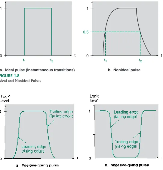
Figure 1.8 shows the forms of both an ideal and a nonidealpulse.Therising and falling edgesof an ideal pulse are vertical. That is, the transitions between logic HIGH and LOW levels are instantaneous. There is no such thing as an ideal pulse in a real digital circuit. Cir-cuit capacitance and other factors make the pulse more like the nonideal pulse in Figure 1.8b. Pulses can be either positive-going or negative-going, as shown in Figure 1.9. In a pos-itive-going pulse, the measured logic level is normally LOW, goes HIGH for the duration
FIGURE 1.8
Ideal and Nonideal Pulses
a. Ideal pulse (instantaneous transitions) t 1
0
t1 t2
t 1
0
t1 t2
b. Nonideal pulse 0.5
of the pulse, and returns to the LOW state. A negative-going pulse acts in the opposite di-rection.
Nonideal pulses are measured in terms of several timing parameters. Figure 1.10 shows the 10%, 50%, and 90% points on the rising and falling edges of a nonideal pulse. (100% is the maximum amplitudeof the pulse.)
FIGURE 1.10
Pulse Width, Rise Time, Fall Time
FIGURE 1.11 Example 1.16: Pulse
The 50% points are used to measurepulse widthbecause the edges of the pulse are not vertical. Without an agreed reference point, the pulse width is indeterminate. The 10% and 90% points are used as references for therise and fall times,since the edges of a nonideal pulse are nonlinear. Most of the nonlinearity is below the 10% or above the 90% point.
❘❙❚ EXAMPLE 1.16 Calculate the pulse width, rise time, and fall time of the pulse shown in Figure 1.11.
SOLUTION From the graph in Figure 1.11, read the times corresponding to the 10%,
50%, and 90% values of the pulse on both the leading and trailing edges.
Leading edge: 10%: 2 s Trailing edge: 90%: 20 s
50%: 5 s 50%: 25 s
S U M M A R Y
1. The two basic areas of electronics are analog and digital electronics. Analog electronics deals with continuously vari-able quantities; digital electronics represents the world in discrete steps.
2. Digital logic uses defined voltage levels, called logic levels, to represent binary numbers within an electronic system. 3. The higher voltage in a digital system represents the binary
digit 1 and is called a logic HIGH or logic 1. The lower volt-age in a system represents the binary digit 0 and is called a logic LOW or logic 0.
4. The logic levels of multiple locations in a digital circuit can be combined to represent a multibit binary number. 5. Binary is a positional number system (base 2) with two
digits, 0 and 1, and positional multipliers that are powers of 2.
6. The bit with the largest positional weight in a binary number is called the most significant bit (MSB); the bit with the smallest positional weight is called the least sig-nificant bit (LSB). The MSB is also the leftmost bit in the number; the LSB is the rightmost bit.
7. A decimal number can be converted to binary by sum of powers of 2 (add place values to get a total) or repeated divi-sion by 2 (divide by 2 until quotient is 0; remainders are the binary value).
8. The hexadecimal number system is based on 16. It uses 16 digits, from 0–9 and A–F, with power-of-16 multipliers. 9. Each hexadecimal digit uniquely corresponds to a 4-bit
nary value. Hex digits can thus be used as shorthand for bi-nary.
10. A digital waveform is a sequence of bits over time. A wave-form can be periodic (repetitive), aperiodic (nonrepetitive), or pulsed (a single variation and return between logic levels.) 11. Periodic waveforms are measured by period (T:time for one cycle), time HIGH (th), time LOW (tl), frequency (f:number of cycles per second), and duty cycle (DCor %DC:fraction of cycle in HIGH state).
12. Pulse waveforms are measured by pulse width (tw: time from 50% of leading edge of 50% of trailing edge), rise time (tr: time from 10% to 90% of rising edge) and fall time (tf: time from 90% to 10% of falling edge).
❘❙❚❘❙❚❘❙❚❘❙❚❘❙❚❘❙❚❘❙❚❘❙❚❘❙❚❘❙❚❘❙❚❘❙❚❘❙❚
G L O S S A R Y
Amplitude The instantaneous voltage of a waveform. Often used to mean maximum amplitude, or peak voltage, of a pulse. Analog A way of representing some physical quantity, such as temperature or velocity, by a proportional continuous voltage or current. An analog voltage or current can have any value within a defined range.
Aperiodic waveform A time-varying sequence of logic HIGHs and LOWs that does not repeat.
Binary number system A number system used extensively in digital systems, based on the number 2. It uses two digits to write any number.
Bit Binary digit.A 0 or a 1. Pulse width:50% of leading edge to 50% of trailing edge.
tw25 s 5 s 20 s
Rise time:10% of rising edge to 90% of rising edge. tr8 s 2 s 6 s Fall time:90% of falling edge to 10% of falling edge.
tf30 s 20 s 10 s ❘❙❚
❘❙❚ SECTION 1.5 REVIEW PROBLEMS
A digital circuit produces a waveform that can be described by the following periodic bit pattern: 0011001100110011.
1.12 What is the duty cycle of the waveform?
1.13 Write the bit pattern of a waveform with the same duty cycle and twice the frequency of the original.
Continuous Smoothly connected. An unbroken series of con-secutive values with no instantaneous changes.
Digital A way of representing a physical quantity by a series of binary numbers. A digital representation can have only spe-cific discrete values.
Digital waveform A series of logic 1s and 0s plotted as a function of time.
Discrete Separated into distinct segments or pieces. A series of discontinous values.
Duty cycle (DC) Fraction of the total period that a digital waveform is in the HIGH state. DC th/T(often expressed as a percentage: %DC th/T 100%).
Edge The part of the pulse that represents the transition from one logic level to the other.
Fall time (tf) Elapsed time from the 90% point to the 10% point of the falling edge of a pulse.
Falling edge The part of a pulse where the logic level is in transition from a HIGH to a LOW.
Frequency ( f ) Number of times per second that a periodic waveform repeats. f 1/TUnit: Hertz (Hz).
Hexadecimal number system Base-16 number system. Hexa-decimal numbers are written with sixteen digits, 0–9 and A–F, with power-of-16 positional multipliers.
Leading edge The edge of a pulse that occurs earliest in time.
Least significant bit (LSB) The rightmost bit of a binary number. This bit has the number’s smallest positional multiplier. Logic HIGH The higher of two voltages in a digital system with two logic levels.
Logic level A voltage level that represents a defined digital state in an electronic circuit.
Logic LOW The lower of two voltages in a digital system with two logic levels.
Most significant bit (MSB) The leftmost bit in a binary num-ber. This bit has the number’s largest positional multiplier.
Negative logic A system in which logic LOW represents bi-nary digit 1 and logic HIGH represents bibi-nary digit 0. Period (T) Time required for a period waveform to repeat. Unit: seconds (s).
Periodic waveform A time-varying sequence of logic HIGHs and LOWs that repeats over a specified period of time.
Positional notation A system of writing numbers in which the value of a digit depends not only on the digit, but also on its placement within a number.
Positive logic A system in which logic LOW represents binary digit 0 and logic HIGH represents binary digit 1.
Pulse A momentary variation of voltage from one logic level to the opposite level and back again.
Pulse width (tw) Elapsed time from the 50% point of the lead-ing edge of a pulse to the 50% point of the traillead-ing edge.
Radix point The generalized form of a decimal point. In any positional number system, the radix point marks the dividing line between positional multipliers that are positive and negative powers of the system’s number base.
Rise time (tr) Elapsed time from the 10% point to the 90% point of the rising edge of a pulse.
Rising edge The part of a pulse where the logic level is in transition from a LOW to a HIGH.
Time HIGH (th) Time during one period that a waveform is in the HIGH state. Unit: seconds (s).
Time LOW (tl) Time during one period that a waveform is in the LOW state. Unit: seconds (s).
Trailing edge The edge of a pulse that occurs latest in time.
P R O B L E M S
Problem numbers set in color indicate more difficult problems: those with underlines indicate most difficult problems.
Section 1.1 Digital Versus Analog Electronics
1.1 Which of the following quantities is analog in nature and which digital? Explain your answers.
a. Water temperature at the beach
b. Weight of a bucket of sand
c. Grains of sand in a bucket
d. Waves hitting the beach in one hour
e. Height of a wave
f. People in a square mile
Section 1.2 Digital Logic Levels
1.2 A digital logic system is defined by the voltages 3.3 volts and 0 volts. For a positive logic system, state which volt-age corresponds to a logic 0 and which to a logic 1.
Section 1.3 The Binary Number System
1.3 Calculate the decimal values of each of the following bi-nary numbers:
a. 100 f. 11101
b. 1000 g. 111011
c. 11001 h. 1011101
d. 110 i. 100001
e. 10101 j. 10111001
1.4 Translate each of the following combinations of HIGH (H) and LOW (L) logic levels to binary numbers using positive logic:
a. H H L H d. L L L H
b. L H L H e. H L L L
1.5 List the sequence of binary numbers from 101 to 1000.
1.6 List the sequence of binary numbers from 10000 to 11111.
1.7 What is the decimal value of the most significant bit for the numbers in Problem 1.6
1.8 Convert the following decimal numbers to binary. Use the sum-of-powers-of-2 method for parts a, c, e, and g. Use the repeated-division-by-2 method for parts b, d, f, and h.
a. 7510 e. 6310
b. 8310 f. 6410
c. 23710 g. 408710
d. 19810 h. 819310
1.9 Convert the following fractional binary numbers to their decimal equivalents.
a. 0.101
b. 0.011
c. 0.1101
1.10 Convert the following fractional binary numbers to their decimal equivalents.
a. 0.01 c. 0.010101
b. 0.0101 d. 0.01010101
1.11 The numbers in Problem 1.10 are converging to a closer and closer binary approximation of a simple fraction that can be expressed by decimal integers a/b.What is the fraction?
1.12 What is the simple decimal fraction (a/b)represented by the repeating binary number 0.101010 . . . ?
1.13 Convert the following decimal numbers to their binary equivalents. If a number has an integer part larger than 0, calculate the integer and fractional parts separately.
a. 0.7510 e. 1.7510
b. 0.62510 f. 3.9510
c. 0.187510 g. 67.8410
d. 0.6510
Section 1.4 Hexadecimal Numbers
1.14 Write all the hexadecimal numbers in sequence from 308H to 321H inclusive.
1.15 Write all the hexadecimal numbers in sequence from 9F7H to A03H inclusive.
1.16 Convert the following hexadecimal numbers to their deci-mal equivalents.
a. 1A0H e. F3C8H
b. 10AH f. D3B4H
c. FFFH g. C000H
d. 1000H h. 30BAFH
1.17 Convert the following decimal numbers to their
hexadeci-mal equivalents.
1.18 Convert the following hexadecimal numbers to their bi-nary equivalents.
1.19 Convert the following binary numbers to their hexadeci-mal equivalents.
Section 1.5 Digital Waveforms
1.20 Calculate the time LOW, time HIGH, period, frequency, and percent duty cycle for the waveforms shown in Fig-ure 1.12. How are the waveforms similar? How do they differ?
1.21 Which of the waveforms in Figure 1.13 are periodic and which are aperiodic? Explain your answers.
1.22 Sketch the pulse waveforms represented by the following strings of 0s and 1s. State which waveforms are periodic and which are aperiodic.
a. 11001111001110110000000110110101
b. 111000111000111000111000111000111
c. 11111111000000001111111111111111
d. 01100110011001100110011001100110
e. 011101101001101001011010011101110
1.23 Calculate the pulse width, rise time, and fall time of the pulse shown in Figure 1.14.
FIGURE 1.12 Problem 1.20: Periodic Waveforms
FIGURE 1.14 Problem 1.23: Pulse
FIGURE 1.15 Problem 1.24: Pulse FIGURE 1.13
Problem 1.21: Aperiodic and Periodic Waveforms
A N S W E R S T O S E C T I O N R E V I E W P R O B L E M S Section 1.1
1.1 An analog audio system makes a direct copy of the recorded sound waves. A digital system stores the sound as a series of bi-nary numbers.
Section 1.3
1.2 64; 1.3. 128; 1.4. 1010000, 1010001, 1010010, 1010011, 1010100, 1010101, 1010110, 1010111; 1.5. 80, 81, 82, 83, 84, 85, 86, 87.
Section 1.4a
1.6 FA9, FAA, FAB, FAC, FAD, FAE, FAF, FB0, 1.7 1F9, 1FA, 1FB, 1FC, 1FD, 1FE, 1FF, 200.
Section 1.4b 1.8 4174310.
Section 1.4c 1.9 1FC9.
Section 1.4d
1.10 1001001101001011. 1.11 C8349.
Section 1.5
25
❘❙❚❘❙❚❘❙❚❘❙❚❘❙❚❘❙❚❘❙❚❘❙❚❘❙❚❘❙❚❘❙❚
❙❚❘❙❚❘❙❚❘❙❚❘❙❚❘❙❚❘❙❚❘❙❚❘❙❚❘❙❚❘❙❚❘❙❚❘❙❚❘❙❚❘❙❚❘❙❚❘❙❚❘❙❚❘❙❚❘❙❚❘❙❚❘❙❚❘❙❚❘❙❚❘❙❚❘❙❚❘❙❚❘❙❚❘❙❚❘❙❚❘❙❚❘❙❚❘❙❚❘❙❚❘❙❚❘❙❚❘❙❚❘❙❚❘❙❚❘❙❚❘❙❚❘❙❚❘❙❚❘❙❚❘❙❚❘❙❚❘❙❚❘❙❚❘❙❚❘❙❚❘❙❚❘❙❚❘❙❚❘❙❚❘❙❚❘❙❚❘❙❚❘❙❚❘❙❚❘❙❚❘❙❚❘❙❚❘❙❚❘❙❚❘❙❚
C H A P T E R
2
Logic Functions and Gates
O U T L I N E 2.1 Basic Logic
Functions
2.2 Logic Switches and LED Indicators 2.3 Derived Logic
Functions 2.4 DeMorgan’s
Theorems and Gate Equivalence
2.5 Enable and Inhibit Properties of Logic Gates
2.6 Integrated Circuit Logic Gates
C H A P T E R O B J E C T I V E S
Upon successful completion of this chapter, you will be able to: • Describe the basic logic functions: AND, OR, and NOT
• Draw simple switch circuits to represent AND, OR and Exclusive OR func-tions.
• Draw simple logic switch circuits for single-pole single-throw (SPST) and normally open and normally closed pushbutton switches.
• Describe the use of light-emitting diodes (LEDs) as indicators of logic HIGH and LOW states.
• Describe those logic functions derived from the basic ones: NAND, NOR, Exclusive OR, and Exclusive NOR.
• Explain the concept of active levels and identify active LOW and HIGH terminals of logic gates.
• Choose appropriate logic functions to solve simple design problems. • Draw the truth table of any logic gate.
• Draw any logic gate, given its truth table.
• Draw the DeMorgan equivalent form of any logic gate.
• Determine when a logic gate will pass a digital waveform and when it will block the signal.
• Describe several types of integrated circuit packaging for digital logic gates.
A
ll digital logic functions can be synthesized by various combinations of the three ba-sic logic functions: AND, OR, and NOT. These so-called Boolean functions are the basis for all further study of combinational logic circuitry. (Combinational logic circuits are digital circuits whose outputs are functions of their inputs, regardless of the order the inputs are applied.) Standard circuits, called logic gates, have been developed for these and for more complex digital logic functions.Electronic Engineers and the American National Standards Institute. It uses a set of sym-bols called rectangular-outline symsym-bols.
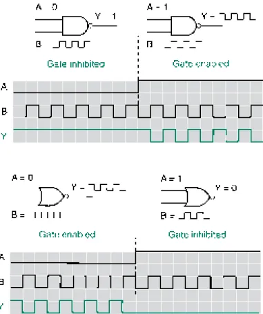
Logic gates can be used as electronic switches to block or allow passage of digital waveforms. Each logic gate has a different set of properties for enabling (passing) or in-hibiting (blocking) digital waveforms. ■
2.1
Basic Logic Functions
Boolean variable A variable having only two possible values, such as HIGH/LOW, 1/0, On/Off, or True/False.
Boolean algebra A system of algebra that operates on Boolean variables. The bi-nary (two-state) nature of Boolean algebra makes it useful for analysis, simplifica-tion, and design of combinational logic circuits.
Boolean expression An algebraic expression made up of Boolean variables and operators, such as AND, OR, or NOT. Also referred to as aBoolean functionor a
logic function.
Logic gate An electronic circuit that performs a Boolean algebraic function.
At its simplest level, a digital circuit works by accepting logic 1s and 0s at one or more in-puts and producing 1s or 0s at one or more outin-puts. A branch of mathematics known as
Boolean algebra(named after 19th-century mathematician George Boole) describes the relation between inputs and outputs of a digital circuit. We call these input and output val-ues Boolean variables and the functions Boolean expressions, logic functions, or
Boolean functions. The distinguishing characteristic of these functions is that they are made up of variables and constants that can have only two possible values: 0 or 1.
All possible operations in Boolean algebra can be created from three basic logic func-tions: AND, OR, and NOT.1 Electronic circuits that perform these logic functions are called logic gates.When we are analyzing or designing a digital circuit, we usually don’t concern ourselves with the actual circuitry of the logic gates, but treat them as black boxes that perform specified logic functions. We can think of each variable in a logic function as a circuit input and the whole function as a circuit output.
In addition to gates for the three basic functions, there are also gates for compound functions that are derived from the basic ones. NAND gates combine the NOT and AND functions in a single circuit. Similarly, NOR gates combine the NOT and OR functions. Gates for more complex functions, such as Exclusive OR and Exclusive NOR, also exist. We will examine all these devices later in the chapter.
NOT, AND, and OR Functions
Truth table A list of all possible input values to a digital circuit, listed in ascend-ing binary order, and the output response for each input combination.
Inverter Also called a NOT gate or an inverting buffer. A logic gate that changes its input logic level to the opposite state.
Bubble A small circle indicating logical inversion on a circuit symbol.
K E Y T E R M S K E Y T E R M S
1Words in uppercase letters represent either logic functions (AND, OR, NOT) or logic levels (HIGH,
Distinctive-shape symbols Graphic symbols for logic circuits that show the func-tion of each type of gate by a special shape.
IEEE/ANSI Standard 91-1984 A standard format for drawing logic circuit sym-bols as rectangles with logic functions shown by a standard notation inside the rec-tangle for each device.
Rectangular-outline symbols Rectangular logic gate symbols that conform to IEEE/ANSI Standard 91-1984.
Qualifying symbol A symbol in IEEE/ANSI logic circuit notation, placed in the top center of a rectangular symbol, that shows the function of a logic gate. Some of the qualifying symbols include: 1 “buffer”; & “AND”; 1 “OR”
Buffer An amplifier that acts as a logic circuit. Its output can be inverting or non-inverting.
NOT Function
The NOT function, the simplest logic function, has one input and one output. The input can be either HIGH or LOW (1 or 0), and the output is always the opposite logic level. We can show these values in atruth table,a list of all possible input values and the output result-ing from each one. Table 2.1 shows a truth table for a NOT function, whereAis the input variable andYis the output.
The NOT function is represented algebraically by the Boolean expression: Y A
This is pronounced “Yequals NOT A”or “YequalsAbar.” We can also say “Yis the complement of A.”
The circuit that produces the NOT function is called the NOT gate or, more usually, theinverter.Several possible symbols for the inverter, all performing the same logic func-tion, are shown in Figure 2.1.
The symbols shown in Figure 2.1a are the standard distinctive-shape symbolsfor the inverter. The triangle represents an amplifier circuit, and the bubble (the small circle on the input or output) represents inversion. There are two symbols because sometimes it is con-venient to show the inversion at the input and sometimes it is concon-venient to show it at the output.
Figure 2.1b shows therectangular-outline inverter symbol specified byIEEE/ANSI Standard 91-1984.This standard is most useful for specifying the symbols for more com-plex digital devices. We will show the basic gates in both distinctive-shape and rectangu-lar-outline symbols, although most examples will use the distinctive-shape symbols.
The “1” in the top center of the IEEE symbol is a qualifying symbol,indicating the logic gate function. In this case, it shows that the circuit is abuffer,an amplifying circuit used as a digital logic element. The arrows at the input and output of the two IEEE symbols show inversion, like the bubbles in the distinctive-shape symbols.
AND Function
AND gate A logic circuit whose output is HIGH when all inputs (e.g.,AAND BANDC) are HIGH.
Logical product AND function.
The AND function combines two or more input variables so that the output is HIGH only ifallthe inputs are HIGH. The truth table for a 2-input AND function is shown in Table 2.2.
K E Y T E R M S
Table 2.1 NOT Function Truth Table
OR Function
OR gate A logic circuit whose output is HIGH when at least one input (e.g.,A ORBORC) is HIGH.
Logical sum OR function.
The OR function combines two or more input variables in such a way as to make the out-put variable HIGH ifat least one input is HIGH. Table 2.4 gives the truth table for the 2-in-put OR function.
K E Y T E R M S
Algebraically, this is written:
Y A B
Pronounce this expression “Yequals A ANDB.”The AND function is similar to mul-tiplication in linear algebra and thus is sometimes called the logical product.The dot be-tween variables may or may not be written, so it is equally correct to writeY AB.The logic circuit symbol for an AND gate is shown in Figure 2.2 in both distinctive-shape and IEEE/ANSI rectangular-outline form. The qualifying symbol in IEEE/ANSI notation is the ampersand (&).
We can also represent the AND function as a set of switches in series, as shown in Fig-ure 2.3. The circuit consists of a voltage source, a lamp, and two series switches. The lamp turns on when switchesAANDBare both closed. For any other condition of the switches, the lamp is off.
FIGURE 2.2
2-Input AND Gate Symbols
Voltage
source Lamp
A
A B B
FIGURE 2.3
AND Function Represented by Switches
Table 2.3 shows the truth table for a 3-input AND function. Each of the three inputs can have two different values, which means the inputs can be combined in 238 different ways. In general,nbinary (i.e., two-valued) variables can be combined in 2nways.
Figure 2.4 shows the logic symbols for the device. The output is HIGH only when all inputs are HIGH.
Table 2.3 3-input AND Function Truth Table
A B C Y
0 0 0 0
0 0 1 0
0 1 0 0
0 1 1 0
1 0 0 0
1 0 1 0
1 1 0 0
1 1 1 1
FIGURE 2.4
3-Input AND Gate Symbols
Table 2.4 2-input OR Function Truth Table
A B Y
0 0 0
0 1 1
1 0 1
The algebraic expression for the OR function is: Y A B
which is pronounced “YequalsAOR B.”This is similar to the arithmetic addition func-tion, but it is not the same. The last line of the truth table tells us that 1 1 1 (pro-nounced “1 OR 1 equals 1”), which is not what we would expect in standard arithmetic. The similarity to the addition function leads to the name logical sum.(This is different from the “arithmetic sum,” where, of course, 1 1does notequal 1.)
Figure 2.5 shows the logic circuit symbols for anOR gate.The qualifying symbol for the OR function in IEEE/ANSI notation is “1,” which tells us thatone or more inputs must be HIGH to make the output HIGH.
The OR function can be represented by a set of switches connected in parallel, as in Figure 2.6. The lamp is on when either switchAOR switchBis closed. (Note that the lamp is also on ifboth Aand B are closed. This property distinguishes the OR function from the Exclusive OR function, which we will study later in this chapter.)
FIGURE 2.5
2-Input OR Gate Symbols
Voltage
source Lamp
A
B
A B
FIGURE 2.6
OR Function Represented by Switches
Like AND gates, OR gates can have several inputs, such as the 3-input OR gates shown in Figure 2.7. Table 2.5 shows the truth table for this gate. Again, three inputs can be combined in eight different ways. The output is HIGH when at least one input is HIGH.
FIGURE 2.7
3-Input OR Gate Symbols
❘❙❚ EXAMPLE 2.1 State which logic function is most suitable for the following operations. Draw a set of
Application switches to represent each function.
1. A manager and one other employee both need a key to open a safe.
2. A light comes on in a storeroom when either (or both) of two doors is open. (Assume the switch closes when the door opens.)
3. For safety, a punch press requires two-handed operation.
SOLUTION
1. Both keys are required, so this is an AND function. Figure 2.8a shows a switch repre-sentation of the function.
Table 2.5 3-input OR Function Truth Table
A B C Y
0 0 0 0
0 0 1 1
0 1 0 1
0 1 1 1
1 0 0 1
1 0 1 1
1 1 0 1
2. One or more switches closed will turn on the lamp. This OR function is shown in Fig-ure 2.8b.
3. Two switches are required to activate a punch press, as shown in Figure 2.8c. This is an AND function.
DC voltage source
Key switch (manager)
Key switch (employee)
Electronic lock
a. Two keys to open a safe (AND)
AC voltage source
Lamp Door switch A
Door switch B
b. One or more switches turn on a lamp (OR)
AC voltage source
Hand switch A
Hand switch B
Solenoid (punch)
c. Two switches are required to activate a punch press (AND) FIGURE 2.8
Example 2.1
❘❙❚
Active Levels
Active level A logic level defined as the “ON” state for a particular circuit input or output. The active level can be either HIGH or LOW.
Active HIGH An active-HIGH terminal is considered “ON” when it is in the logic HIGH state. Indicated by the absence of a bubble at the terminal in distinc-tive-shape symbols.
Active LOW An active-LOW terminal is considered “ON” when it is in the logic LOW state. Indicated by a bubble at the terminal in distinctive-shape symbols.
Anactive levelof a gate input or output is the logic level, either HIGH or LOW, of the ter-minal when it is performing its designated function. Anactive LOWis shown by a bubble or an arrow symbol on the affected terminal. If there is no bubble or arrow, we assume the terminal is active HIGH.
The AND function has active-HIGH inputs and an active-HIGH output. To make the output HIGH, inputsAAND B mustbothbe HIGH. The gate performs its designated func-tion only whenallinputs are HIGH.
The OR gate requires inputAOR input Bto be HIGH for its output to be HIGH. The HIGH active levels are shown by the absence of bubbles or arrows on the terminals.
❘❙❚ SECTION REVIEW PROBLEM FOR SECTION 2.1
A 4-input gate has input variablesA, B, C,and D and outputY.Write a descriptive sentence for the active output state(s) if the gate is
2.1 AND; 2.2 OR.
2.2
Logic Switches and LED Indicators
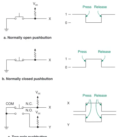
Before continuing on, we should examine a few simple circuits that can be used for input or output in a digital circuit. Single-pole single-throw (SPST) and pushbutton switches can be used, in combination with resistors, to generate logic voltages for circuit inputs. Light emitting diodes (LEDs) can be used to monitor outputs of circuits.
Logic Switches
VCC The power supply voltage in a transistor-based electronic circuit. The term often refers to the power supply of digital circuits.
Pull-up resistor A resistor connected from a point in an electronic circuit to the power supply of that circuit.
Figure 2.9a shows a single-pole single-throw (SPST) switch connected as a logic switch. An important premise of this circuit is that the input of the digital circuit to which it is con-nected has a very high resistance to current. When the switch is open, the current flowing through thepull-up resistorfrom VCCto the digital circuit is very small. Since the current is small, Ohm’s law states that very little voltage drops across the pull-up resistor; the volt-age is about the same at one end as at the other. Therefore, an open switch generates a logic HIGH at point X.
K E Y T E R M S
High input resistance
Vcc
Digital circuit X
a. Circuit b. Logic levels
1
0
Open Closed Open
FIGURE 2.9 SPST Logic Switch
and limits power supply current in the LOW state. Figure 2.9b shows the voltage levels when the switch is closed and when it is open.
Figure 2.10 shows how pushbuttons can be used as logic inputs. Figure 2.10a shows a normally open pushbutton and a pull-up resistor. The pushbutton has a spring-loaded plunger that makes a connection between two internal contacts when pressed. When re-leased, the spring returns the plunger to the “normal” (open) state. The logic voltage at X is normally HIGH, but LOW when the button is pressed.
Vcc
X
a. Normally open pushbutton
Press Release
Vcc
X
c. Two-pole pushbutton
X
Press Release X
b. Normally closed pushbutton
Y
Press Release
N.C. COM
Vcc
Y N.O.
1
0
1
0
FIGURE 2.10
Pushbuttons as Logic Switches
Figure 2.10b shows a normally closed pushbutton. The internal spring holds the plunger so that the connection is normally made between the two contacts. When the but-ton is pressed, the connection is broken and the resistor pulls up the voltage at X to a logic HIGH. At rest, X is grounded and the voltage at X is LOW.
It is sometimes desirable to have normally HIGH and normally LOW levels available from the same switch. The two-pole pushbutton in Figure 2.10c provides such a function. The switch has a normally open and a normally closed contact. One contact of each switch is connected to the other, in an internal COMMON connection, allowing the switch to have three terminals rather than four. The circuit has two pull-up resistors, one for X and one for Y. X is normally HIGH and goes LOW when the switch is pressed. Y is opposite.
LED Indicators
LED Light-emitting diode. An electronic device that conducts current in one di-rection only and illuminates when it is conducting.
A device used to indicate the status of a digital output is thelight-emitting diodeorLED.
This is sometimes pronounced as a word (“led”) and sometimes said as separate initials (“ell ee dee”). This device comes in a variety of shapes, sizes, and colors, some of which are shown in the photo of Figure 2.11. The circuit symbol, shown in Figure 2.12, has two terminals, called the anode (positive) and cathode (negative). The arrow coming from the symbol indicates emitted light.
Anode Cathode
FIGURE 2.11 LEDs
FIGURE 2.12
Light-Emitting Diode (LED)
The electrical requirements for the LED are simple: current flows through the LED if the anode is more positive than the cathode by more than a specified value (about 1.5 volts). If enough current flows, the LED illuminates. If more current flows, the illumination is brighter. (If too much flows, the LED burns out, so a series resistor is used to keep the current in the required range.) Figure 2.13 shows a circuit in which an LED illuminates when a switch is closed.
Figure 2.14 shows an AND gate driving an LED. In Figure 2.14a, the LED is on whenYis HIGH (5 volts), since the anode of the LED is more positive than the cathode.
Vcc
470
FIGURE 2.13
Condition for LED Illumination
A Y
B
470
a. LED on when Y is HIGH
A Y
B
470
Vcc
b. LED on when Y is LOW FIGURE 2.14