MOSFET STEREO AUDIO AW>LIFIER DESIGN
RUDY THADDEUS
UNIVERSITI MALAYSIA SARAWAK 1997
11{
6565 ASS
R917
1997
BORANG PENYERAHAN TESIS
SESI PENGAJIAN: Tahun Akhir
mengaku meDlbenarkan tesis ini elisimpan di Pusat Khidmat Maklumat, Universiti Malaysia Sarawak dengan Ayarat·syarat seperti berikut:
L l-lakmilik kertas projek adalah eli bawah nama penu.lis melainkan renulisan sebagai projek bersarna dan dibiayni oleh UNIl\1:AS. hakmiliknya adalahkepunyaan UN1M AS.
2. Naskhah salinan di dalam bentuk kertas atau mikro hanya boleh dibuat dengan kebenaran bertu.lis
<iaripada penulis.
3. Pusal: Khidmat Maklun1l11 Akademik, UN1MAS dibellarkan membuat salinan unt:uk pengajian mel'cka.
4. Kertas projek hanya boleh diterbit.kan dengan kebenaran pcnulis. Bayaran royalti adalah mengikut kadal' yang dipcrsetujui kcl.ak.
5. * Saya mcmbenarkanJtidak membenllrkan Perpust.akaan membuat salinall kcrtas projek ini sebagai bahan pcrtukaran di antm'a institusi pengajian tingJ,.].
6. ** Sila tandakan ( )
SULIT (Mengalldungi maklumut yang berdarjah kcsel".IDtltan "tau kepentingllJ1 Malaysia seperti yang t.ermaktub di dalam AKTA RAHSfA RAS~n 1972)
T8RHAD (Menglllldunl(i mllklumat. TEH,"V\D ),ung telah dilent.ukllll olch ol'gunis".iibmlan pf'nyelirlikllI1 rli mlln" penyelidiklln dij"lank.. n)
G
TIDAl, TEHl-fAD.jYY
(TANDATANGAN PENULIS) (TANDATANGAN PENYf~LlA)
Dr. Mobamad Kadim Hj. Suaidi
Kctua Program . '
Alamat Tetap: I'~"" Q'1 L10C(}<Q, K eJuru · t e,~, _ on r;-l...lrt!"('\" ".;i~ , (111; T:l··.: ~~C'.imkasl ltO 000 S"" t:AI\ , Sal..o~,
Nama Penyelia
\
Tarikh: _
l
<1)-t-=----<,O(t---+-17CATA'rAN * Potong yang tidak bcrkenaan.
** Jika Kertas Projek ini SULlT at.au TERfL\D. sila lalllpirkan surat fiaripada pihak
berkua~a/organisasi berkcnaan dengan mcnycrt.akan sekali tempoh kertas projek. lni perlu dikelaskan sebagai SULIT atau TERRill.
This Thesis was read and approved by:
• • • • • • • • • • • • ' " " 0 • • • • • • ' " '" •• • ' 0 ' '" •••
Dr. Mohammad Kadim Suaidi Date
Supervisor
I
/
Pusar Khidrnar /W.
UNIVERSITI MALak'urnar Akadtmik
AYSIA SARAWAK
P . I(HIDMAT MAI(L.UMAT
1I
0000072692IIIiiiilllili
/
MOSFET STEREO AUDIO AMPLIFIER DESIGN
RUDY THADDEUS
This Thesis is presented to the
Faculty of Engineering, Universiti Malaysia Sarawak As to Fulfill One of the Requirement
for Bachelor (Hons) of Engineering
( Electronic and Telecommunication Engineering) 1997
,...
1.
For My Beloved Family
1\
ACKNOWLEDGMENTS
I would like to give a special thanks to my supervisor, Dr. Mohammad Kadim Suaidi for giving his knowledge and giving chance for me to do this thesis project.
Also, thanks to all my colleagues who have helped me to finish this thesis especially to Mr. Awang Musa bin Hassan who had kindly let me use his computer and to Mr.BadrulHisham for letting me use his printer.
III
ABSTRAK
Pada masa kini penggunaan sistem amplifier audio stereo kuasa tinggi telah digunakan dengan meluas mengikut teknologi semasa. Sistem ini boleh didapati di pasaran dalam berbagai bentuk dan kelebihan. Kelebihan-kelebihan yang biasa diambil berat ialah dari segi penghasilan bunyi sistem tersebut dan kebolehannya untuk memainkan pelbagai alat-alat muzik. Tesis Inl
membincangkan dalam mereka sebuah modul sistem audio amplifier stereo MOSFET. Ciri-ciri dan faktor-faktor yang mempengaruhi spesifikasi alat diperbincangkan. Kaedah dan masalah yang dihadapi dalam pembinaan sistem ini juga akan turut diperbincangkan.
IV
ABSTRACT
Today, the high performance stereo audio amplifiers have been widely use according to the technology. The system can be found in the market in various forms and advantages. The considerable advantages of this system are in terms of its output sound and application to many musical input devices. The purpose of this thesis is to explain the building of a MOSFET stereo audio amplifier module. The characteristics and factors that has effect on the specifications of the system are discus. Method and problems that arise in constructing it are also discus.
v
(
\
\CONTENTS
Chapter 1. Introduction
1.0 Audio Amplifier Classification 1.1 Audio Amplification Principle 1.2 Common-Collector Audio Amplifiers 1.3 Operating Point of Audio Circuits 1.4 Power Amplifiers
1.5 Stereo Sound 1.6 Discussion
2. Pre-Amplifier Input Module 2.0 Introduction
2.1 Module Circuit
2.2 Module Specifications 2.3 Module Components 2.4 Construction
3. Tone Control Module 3.0 Introduction 3.1 Module Circuit
3.2 Module Specifications 3.3 Module Circuit Components 3.4 Construction
4. Power Supply Module 4.0 Introduction 4.1 Circuit Layout 4.2 Module Circuit 4.3 Module Components 4.4 Construction
5. MOSFET Power Amplifier 5.0 Introduction
.1 General Specifications 5.2 MOSFET Power Amplifier 5.3 Module Circuit
5.4 Module Specifications
VI
· l Akadtmik Kh' dmat Makluma
pusat , MALAYSlA SARAWA!/..
UNIVERSlTl
Page
1 1 3 3 6 11 14
16 18 27 28 29
30 32 36 36 37
38 38 44 45 46
47 48 52 55 58
/
5.5 Module Circuit Components 5.6 Construction
6. Discussion 6.0 Introduction 6.1 Discussion
6.2 Recommendations 6.3 Conclusion
Appendices References
59 60
62 62 66 66 68 71
vii
....
TABLE LIST
Table Page
1. Typical microphone sensitivity ranges.
/
VlIl
23
\
FIGURE LIST
Figure Page
1. Audio amplification and emitter-feedback basics. 2 2. Audio operating-point classifications· 7 3. Audio operating-point classifications2 7 4. Valve amplifier with 15W rating, 1938. 8 5. Valve amplifier with 15W rating, 1960. 8 6. Quad 405-2 100W+ 100W transistor stereo amplifier, 1988. 9 7. Output voltage and current waveforms for feedback 10
amplifier exhibiting pure current clipping.
8. Two channel stereo from two loudspeakers. 12
9. An op-amp pre-amplifier stage. 17
10. Pre-amplifier input module circuit. 19
11. Equalisation link interconnection. 20
12. Magnetic PU response curve. 26
13. Ceramic PU response. 27
14. A basic tone control. 30
15. Tone control module circuit. 31
16. Two basic characteristic of tone control. 32
17. Input / Output Wiring. 33
18. Treble and bass control potentiometers. 34
19. Boost and cut. 35
IX
20. Volume control potentiometer wiring. 35
21. Simple half-wave rectifier system. 39
22. Half-wave rectifier output ripple. 39
23. Full-wave rectifier systems. 41
24. Additional PSU layouts. 42
25. PSU module circuit. 44
26. Power MOSFET operating characteristics. 53
27. MOSFET symbol. 54
28. Typical Power MOSFET Output Characteristic. 54 29. Circuit diagram for single channel MOSFET power
amplifier. 56
30. Power MOSFET package. 57
31. Inductor L1. 58
/
x
I
II
\
\
,....
Q
AC dB PC diJdt ESR HF Hz IC
MOSF~T
PA PCB PSU PU r.m.s.
RF RIAA SNR TID Vout W
ABBREVIATIONS
Ohm (resistive unit) Alternating current Decibal (unit for gain) Direct current
Difference of current with respect to time Equivalent series resistance
fIigh tfeq~ency
Hertz (Frequency unit) Integr&ted circuit , '
Metal-oxiQe semiconductor Field-effect transistor Power amplifier
Printed circuit board Power supply unit Pick-up
Root mean square Radio Frequency
Record Industry Association of America Signal to noise ratio
Transient intermodulation distortion Output Voltage
Watt (unit for power)
Xl
APPENDICES LIST
Page
1. Printed circuit for pre-amplifier module 68
2. Printed circuit for tone control module 69
3. Printed circuit for MOSFET power amplifier module 70
I /
\
xii
/
\
Pusat Khidmat Maklumat Akademik UNIVERSITI MALAYSIA SARAWAX
CHAPTER 1
INTRODUCTION
This chapter covers the basic about audio amplifiers that related to the project of the designing of a MOSFET stereo audio amplifier system. The basic about audio amplifier will be briefly explained along with the classifications include and also some considerations to the output signal ofthe power amplifier.
Here, also some introduction to the concept of the stereo sound will be briefly discussed.
1.0 Audio Amplifier Classifications
Audio amplifiers are classified in many ways. The two most common methods are by operating-point or bias-point and circuit connections. Audio amplifiers are also classified by their function or purpose (voltage amplifier, power amplifier, etc.).
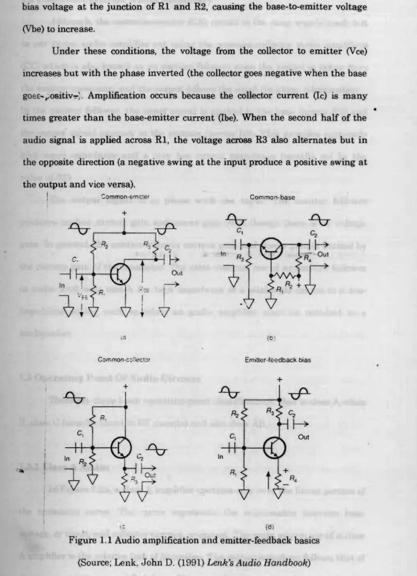
1.1 Audio Amplification Principle
Figure 1.1 shows the typical common-emitter (CE) audio circuit. Under no signal (or quiescent) conditions, current flows in the input circuit (across R1), causing a steady value of current to flow in the output circuit (across R3).
A voltage is developed across R 1 during the first half of the audio signal a plied to the input. This voltage, positive at the base end of R1, adds to the
I /
bias voltage at the junction of Rl and R2, causing the base-to-emitter voltage (Vbe) to increase.
Under these conditions, the voltage from the collector to emitter (Vee) increases but with the phase inverted (the collector goes negative when the base
go;::£~ ~ositiv~> Amplification occurs because the collector current (Ie) is many times greater than the base-emitter current (Ibe). When the second half of the •
audio signal is applied across Rl, the voltage across R3 also alternates but in the opposite direction (a negative swing at the input produce a positive swing at the output and vice versa).
!
Sommon·"ml,:er Common-base+
,in
-i
c. ~
OUI c~,
I ,--
I .
J
I
!V ..
iV
~
I;; (b ]
Common·c·:·::ect'Jr Emiller-feedback bias
+
-%-
+(di
Figure 1.1 Audio amplification and emitter-feedback basics (Source; Lenk, .John D. (1991) Lenk's Audio Handbook)
,
I
\,
1.2 Common-Collector Audio Amplifiers
Although, the common-emitter (CE) circuit is the most widely used, but in our stereo audio amplifier are using the common-collector audio amplifiers (CC) which is also known as an emitter follower since the output is taken from the emitter resistance, and the output follows the input (in phase relationship).
In the emitter follower, the input signal is applied to the base (across R2) and
the output signal appears at the emitter (across R3). This provides extremely high input impedance and a very low output impedance (usually set by the
value of R3).
The output signal is in phase with the input. The emitter follower produces modest current gain and power gain even though there is no voltage gain. In general, the emitter follower current gain and power gain is limited by the.current gain of the transistor. The most common use of an emitter follower in audio work is to match the high impedance of a solid-state circuit to a low- impedance device, such as when an audio amplifier must be matched to a loudspeaker.
1.3 Operating Point Of Audio Circuits
There are three basic operating-point classifications, that is class A, class B, class C (usually found in RF circuits) and also class AB.
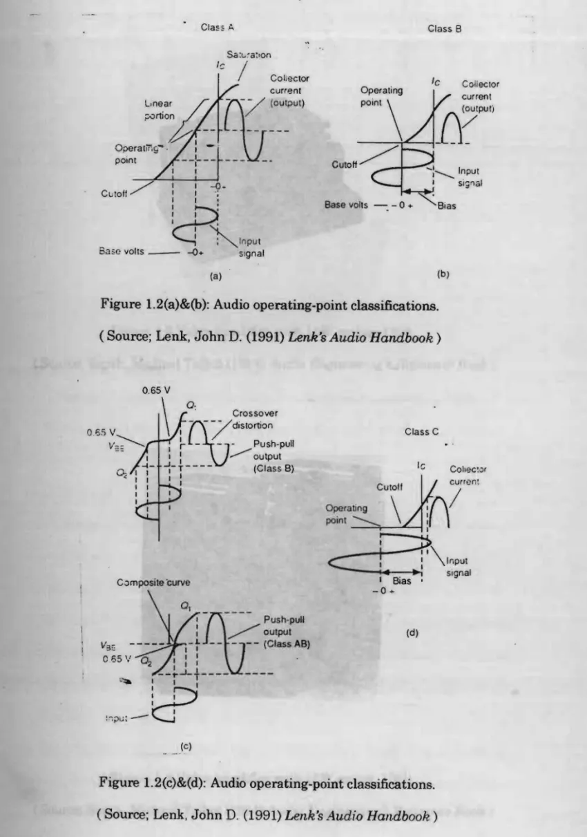
1.3.1 Class A Audio
In Figure 1.2a, a class A amplifier operates only over the linear portion of the transistor curve. The curve represents the relationship between base voltage, or input, and collector current, or output. The main advantage of a class A amplifier is the relative lack of distortion. The output waveform follows that of the input, except in amplified form. The main disadvantages of class A circuits
3
,/
/
\
are relative inefficiency Gower power output for a high-power input that must be
dissipated by the transistor) and the inability to handle large signals. Class A amplifier is always below 35% efficient. If the power input to a class A amplifier is 1 W, the output is less than 0.3W.
The input voltage swing of a class A audio amplifier is limited by the output voltage swing and the voltage amplification factor. For example, if the
output is limited to
±
10 V and the voltage amplification factor is 100, the input is limited to ± 0.1 V (100m V).Because of these limitations, class A audio circuits are generally used as a voltage amplifiers rather than power amplifiers. Typically, a class A amplifier stage is used ahead of a power amplifier stage.
1.3.2 Class B Audio
A class B amplifier operates only on one-half of the input signal (Figure 1.2b). Class B is produced when the base-emitter bias is set so that the operating point coincides with the transistor cut-ofIpoint. When the input signal voltage is zero, there is no flow of collector current.
There is considerable distortion if a single transistor is operated as class B. This is because the waveform of the resulting collector current resembles that of one input half-cycle and does not resemble the complete wavwform at the
input. Class B is generally used when two transistors are connected in push
pull. This makes it possible to reconstruct an output waveform that resembles the full waveform of the input.
The peak output voltage swing of a class B amplifier is slightly less than the supply voltage. Since the output appears only on half-cycles, it is possible to operate class B amplifiers at a higher current (or power) rating than class A with equal factors. The peak output of a class B amplifier is equivalent to the p
4
I /
p output of class A amplifier. So, if two transistors are connected in push-pull
and operated as class B, the output voltage can be twice that of class A. Due to the voltage and power factors, class B amplifiers are generally used as power amplifiers rather than voltage amplifiers.
In a typical audio amplifier using discrete components, two push-pull transistors are operated in class B, preceded by a single class A stage. The class A stage provides voltage amplification, whereas the class B stage produces the necessary power amplification.
1.3.3 Class AB audio
Class AB operation is used in audio amplifiers to minimize the effects of crossover distortion, shown in Figure 1.2c. In pure class B, the transistor remains cut off at very low signal inputs and turns on with a large input signal.
In class B push-pull operation, during the instantaneous pause when one transistor stops conducting and the other transistor starts conducting, the
output waveform is distorted. This instantaneous cutoff of collector current can also set up large voltage transients equal to several times the supply voltage, possibly, resulting in transistor breakdown.
By using class AB amplifier these undesired effects can be mmlmlze, where the transistors are forward biased enough for a small amount of collector current to flow at the Q-point, and there is no cutoff turn on.
1.3.4 Class C audio
The characteristic of a typical class C amplifier are shown in Figure 1.2d.
The transistor is reversed biased well below the cutoff point and that there is collector-current flow for only a portion of half the input signal. From Figure 1.2d obviously shows the waveform of the output signal cannot resemble to the
5
I /
input signal even if it is restored by push-pull operation such as in class A or AB. Class C is limited to those applications where distortion is of no concern which usually 'means RF circuits rather than audio circuits.
1.4 Power Amplifiers
1.4.1 History
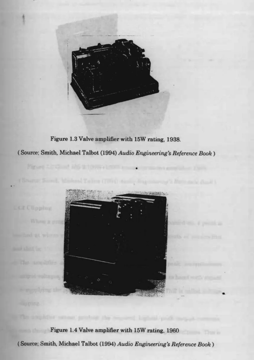
In Figure 1.3 shows a British 14W amplifier of 1938 vintage, which is used for domestic high quality sound reproduction. The retail price at that time is £20 which yield a figure of approximately 0.7W per £ 1. In Figure 1.4 shows the Quad 15W valve amplifier cost about £22 in 1960, which also gives a figure of around 0.7W per £ 1. The purchasing value of the pound had meanwhile had fallen by a factor of at least 2, so that the maintenance of the 0.7W per £ 1 clearly resulted mainly from the more economical design of the later amplifier, which employed beam tetrodes with negative feedback to obtain low distortion and a low hum level.
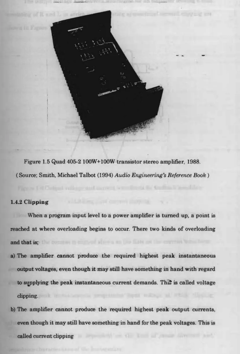
However, the advent of transistors enabled a far more striking economy of engineering to be effected. The Quad 405-2 transistor amplifier shown in Figure 1.5 gives a total output of 200W, sold in 1988 for around £300, again yielding a figure of about 0.7W per £ 1. But the large financial inflation of that time since 1960 clearly shows the true cost per watt with modern semiconductor technology is indeed down and clearly shows a major engineering advance.
6
\
Class A Class B
Sa:u~a:lon
I~ /
Coliector Ie Coliector
current
CUloH/ :
Base volts ---: - 0 +
Iml,
I I •I :
~ lnPlJt
Basc volts - ~+ signal
(a) (b)
Figure 1.2(a)&(b): Audio operating-point classifications.
( Source; Lenk, John D. (1991) Lenks Audio Handbook)
Crossover
.ry} /
distortion Class C~ - - - Push-pull
: • ~output
~-
+----
(Class B) Ie Coilec~.)r current I ••c
C~mposite 'curve
-0+
o. _ ___ _
.~ Push-pull
: / ' o u t p u l (d)
Ii' -3:; - - - - - I I -1. - - - - - (Class AS)
0.65 If ~
I:: .
--~...Lt----
---
.~
; b
:,;:>1.;;
IT
(c)
Figure 1.2(c)&(d): Audio operating-point classifications.
( Source; Lenk, John D. (1991) Lenk's Audio Handbook)
7
Figure 1.3 Valve amplifier with 15W rating, 1938.
(Source; Smith, Michael Talbot (1994) Audio Engineering's Reference Book)
•
Figure 1.4 Valve amplifier with 15W rating, 1960
(Source; Smith, Michael Talbot (1994) Audio Engineering's Reference Book)
8
/
Figure 1.5 Quad 405-2 100W+ lOOW transistor stereo amplifier, 1988.
(Source; Smith, Michael Talbot (1994) Audio Engineering's Reference Book)
1.4.2 Clipping
When a program input level to a power amplifier is turned up, a point is reached at where overloading begins to occur. There two kinds of overloading and thatis;
a) The amplifier cannot produce the required highest peak insta ntaneous output voltages, even though it may still have something in hand with regard to s~pplying the peak instantaneous current demands. Thl~ is called voltage clipping.
b) The amplifier cannot produce the required highest peak output currents, even though it may still have something in hand for the peak voltages. This is called current clipping
<)