COMMUNICA
TION
Tuning the Tunneling Rate and Dielectric Response of
SAM-Based Junctions via a Single Polarizable Atom
Dandan Wang, Davide Fracasso, Argo Nurbawono, Harshini V. Annadata,
C. S. Suchand Sangeeth, Li Yuan, and Christian A. Nijhuis*
D. Wang, Dr. D. Fracasso, H. V. Annadata, Dr. C. S. S. Sangeeth, L. Yuan, Prof. C. A. Nijhuis Department of Chemistry
National University of Singapore
3 Science Drive 3, Singapore 117543, Singapore E-mail: [email protected]
D. Wang, Dr. D. Fracasso, H. V. Annadata, Dr. C. S. S. Sangeeth, L. Yuan, Prof. C. A. Nijhuis
Centre for Advanced 2D Materials and Graphene Research Centre National University of Singapore
6 Science Drive 2, Singapore 117546, Singapore Dr. A. Nurbawono
Department of Physics National University of Singapore
2 Science Drive 3, Singapore 117551, Singapore
DOI: 10.1002/adma.201502968
0
J=J e−βd (1)
Cahen and co-workers[7,8,25] were able to tune the effective
barrier height by changing the dipole moment of the molecules
(µ in D) using semiconducting bottom electrodes. In contrast,
Whitesides and co-workers showed that in EGaIn-based
junc-tions (see Figure 1) the tunneling rates are insensitive to a
large number of terminal groups including simple aromatic,[9]
polar,[10] and acidic groups.[11] McCreery and co-workers[6] also
found that the tunneling rates are remarkably insensitive to a broad range of chemical groups. On the other hand, subtle changes in the monolayer structure did cause a significant change in the electrical properties of junctions. For instance,
odd–even effects in the tunneling rates as a function of n
have been observed in junctions with SAMs of SCnX (where
X = CH3,[12] phenyl,[13] or ferrocene[14] or replacing a C–H unit
by a N in SAMs of oligo(phenylene)s result in clear change of
the transition voltage.[15] The tunneling rates in EGaIn
junc-tions are sensitive to some terminal groups including
ferro-cene,[16] bipyridyl,[17] and naphthoquinone[18] (all these groups
induced rectification). In addition, examples of junctions with conjugated systems showed quantum interference effects,
which could be theoretically explained,[19,20] or tunneling rates
that could be related to experimentally determined tunneling
barrier heights and widths.[21] These examples illustrate the
dif-ficulty in predicting how the SAM structure will influence the electrical properties of SAM-based junctions.
A major challenge in the organic semiconductor industry is
the development of high-capacitance gate dielectrics.[26] In order
to obtain the required drive currents at relatively low operating voltages for field-effect devices, thin gate dielectrics with high capacitances and low leakage currents are necessary. SAMs have been proposed as attractive candidates since they are thin,
but their εr values (<4) are in general too low for most
applica-tions. The capacitance of a SAM (CSAM in µF cm−2) sandwiched
between two electrodes—a SAM-based tunneling junction—is
proportional to εr and inversely proportional to dSAM (in nm,
the thickness of the SAM) as given by Equation 2 where ε0 is
the permittivity of free space and Ageo (in cm2) is the
geomet-rical area of the electrodes.[27] We note that due to the small tilt
angle of the SAMs on Ag of 11°,[28] the value of d
The leakage current that flows across such junctions is given
by Equation 1 and hence a trade-off exists as increasing CSAM
by lowering dSAM results in large leakage currents.[29] For this
One of the original promises of molecular electronics was that it would make it possible to tune the electronic func-tion of devices at the molecular scale, with a seemingly end-less number of possibilities given the great synthetic freedom
with which the properties of the molecules can be tuned.[1–5]
To achieve this goal, one needs to understand which kinds of chemical groups do affect the electrical characteristics of the junctions and how they do that. Recent studies showed that in practical test beds of the form electrode–SAM–electrode (where SAM refers to a self-assembled monolayer), it is not always straightforward to predict which kind of chemical
functionali-ties will affect the electrical response of the junctions.[6–21] In
addition, systematic experimental investigations concerning the dielectric response of molecular junctions are rare despite their promising potential in applications requiring high-capacitance
gate dielectrics.[22–24] Here, we show that in tunneling
junc-tions with SAMs of S(CH2)11X (SC11X with X = H, F, Cl, Br,
or I), the tunneling rate increases by three orders of
magni-tude and the relative dielectric constant εr by a factor of 4 with
increasing polarizability of X, which also results in a decrease of the highest occupied molecular orbital–lowest unoccupied molecular orbital (HOMO)–(LUMO) gap (and the tunneling barrier height). Hence, introducing polarizable groups seems to be an attractive method to control both the tunneling rate and the dielectric response of two-terminal molecular junctions.
By far most studies have focused on structure–property
rela-tions by measuring tunneling currents (J in A cm−2) across
SAM-based junctions and interpret the data in terms of a
gen-eral tunnel equation (Equation 1) where β (in Å−1) is the
tun-neling decay coefficient, d (in nm) is the tunneling barrier
width (the length of the molecule), and J0 is the current that
COMMUNICA
TION
reason, it is important to increase εr. Recently, Ratner and
co-workers[24] calculated that the SAM properties such as the
surface coverage, molecular tilt angle, or conjugation, have
a large effect on the value of εr. They showed that densely
packed SAMs, with small tilt angles, and with highly
polariz-able groups, may have large values of εr. For example, they
cal-culated that εr increases from 5.1 to 8.7 for monosubstituted
trans-polyacetylene SAMs when the terminal hydrogen was
replaced by groups with increasing polarizability (the highest εr
was found for SAMs with iodine atoms). How the polarizability
of a single atom changes the values of J and εr in a SAM-based
device has not been experimentally determined yet.
In this work, we aim to address the following question: how
does a change in the polarizability (α in Å3) of a single atom in
a SAM-based junction changes the value of εr and the
meas-ured value J and how significant would this change be? We
used eutectic gallium–indium (GaOx/EGaIn, where GaOx is
0.7 nm thick native oxide of predominantly β-Ga2O3) as a
non-invasive soft top-electrode[30,31] in junctions with the SAMs
sup-ported by template-stripped (TS) Ag that were annealed before
TS (AgA-TS).[32] These bottom electrodes have large grains and
are ultra-smooth (Figure S3, Supporting Information). Figure 1
shows these junctions of the form AgA-TS–SC
11X//GaOx/EGaIn
schematically and the relative sizes of the substituents X = H,
F, Cl, Br, or I. In these junctions, we changed α of a single atom
while keeping the changes to the permanent dipole, the surface coverage, tilt angle of the SAM, and the SAM thickness, to a
minimum. Below we describe how this change in α changes
the tunneling rates and the dielectric constant, but first we dis-cuss the SAM structure in more detail.
The SAMs were derived from the corresponding thiols (the synthetic details are described on page S2–S9 in the Supporting Information) and characterized by angle-resolved X-ray photo-electron spectroscopy (AR-XPS), ultraviolet photophoto-electron spec-troscopy (UPS), and contact angle (CA) measurements. The
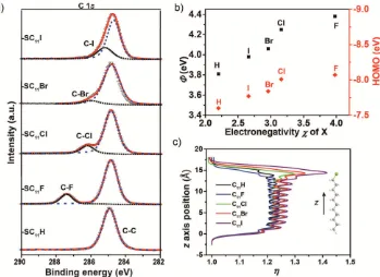
results are given in Table1 and Figure2 (see page S15–S22 in
the Supporting Information for more details). Figure 2a shows
the C 1s spectra recorded at incident angle (90°). The spectra
are dominated by the two signals associated with the aliphatic carbon and the carbon next to the halogen, which shifts to lower
binding energy with decreasing electronegativity χ of X. From
the AR-XPS data, we determined dSAM and the surface
cov-erage (ΓSAM in mol cm−2). All SAMs are ≈1.5 nm thick (except
for X = H which is 1.3 nm thick), which is consistent with the
molecular lengths estimated from CPK models. The values of
ΓSAM of 1.1 × 10⁻⁹ mol cm−2 are close to theoretical values for
SAMs on Ag with a ( 7× 7) 10.9R ° packing.[33] From these
data, we conclude that the SC11X thiolates form densely packed
SAMs, which are standing up with small tilt angles (likely close
to ≈11° as has been reported before for n-alkanethiolate SAMs
on Ag).[33]
Figure 2b shows the work function (Φ in eV) and the HOMO
(in eV) plotted against χ, the former decreases by 0.40 eV with
increasing atom number Z of the halogen. We ascribe this
decrease in Φ to the decrease in dipole moment as χ decreases
with increasing Z.[34–37] The energy of the highest occupied
molecular orbital (EHOMO in eV, which is also called the
ioniza-tion potential), calculated as the sum of the HOMO onset and
Φ, increases as χ increases (Table 1) while the HOMO-onset
values remain constant. This observation can be explained
as the value Φ can change without changing the energy level
alignment (i.e., the value of EHOMO) because the electrostatic
change as a result of the change in dipole by varying χ is
con-fined within in SAM (i.e., here the electronic structure of the
www.advmat.de
www.MaterialsViews.com
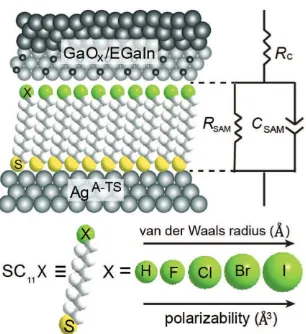
Figure 1. Schematic illustration of the AgA-TS–SC
11X//GaOx/EGaIn
junc-tion with X = H, F, Cl, Br, or I. The equivalent circuit, van der Waals (vdW) radius of X, and how α depends on X are also indicated. RC is the total contact resistance, RSAM is the SAM resistance, CSAM is the capacitance of the SAM (determined from the constant phase element, CPE).
Table 1. The properties of the SAMs.
SAMs dSAMa)
a)Determined by AR-XPS; the error represents the error of the fit, for d
SAM the error was 0.01 nm (see page S16–S18 in the Supporting Information); b)Determined by
UPS; the error in the energy resolution was 0.05 eV; c)Determined from TD-DFT;[60] see page S28–S29 in the Supporting Information; d)Determined using the experimental
HOMO values and theoretical Eg values; e)The polarizability of the respective molecule in the gas phase calculated by DFT (see page S24–S25 in the Supporting
Informa-tion); f)Dispersive γ
sD and polar γsP components of the surface energy estimated from CA measurements (see page S23 in the Supporting Information for the errors); g)We
COMMUNICA
TION
bottom electrode–SAM interface is not affected by the terminal
group, only the work function).[36–38]
We determined the dispersive (γsD in mN m−1) and polar (γsP
in mN m−1) components of the surface energy of the SAMs by
CA measurements with two liquids (H2O and CH2I2) using
Fowkes’ method.[39] Table 1 shows that the values of γ
sD are
about a factor ten larger than the values of γsP. We determined
the value of α by density functional theory (DFT) calculations
(using B3LYP functionals and the 6-311G** basis set) of gas phase molecules and an empirical method based on an addi-tive approach of the atomic polarizabilities (see page S24–S25 in the Supporting Information for details). The DFT calculations
resulted in values of α that were consistently ≈10% lower than
those obtained by the additive method (Table S2, Supporting Information) from which we conclude that both approaches give reasonable values. Here we used the values obtained by the DFT calculations. To understand the dielectric distribution at the molecular scale, we performed DFT calculations similar to those reported by Ratner and co-workers (see page S26 in the
Supporting Information).[24] Figure 2c shows the planar
aver-aged local dielectric constant (η) profiles for C11X monolayers,
which also include a simple hydrocarbon chain (CnH2n+2 with
n = 11) to underline the effect of X moieties. Similar to the
results described by Ratner and co-workers, the hydrocarbon
alkyl chain has a symmetric distribution of η along the length of
the molecule concentrating towards the center. The halogenated hydrocarbons differ from each other only at the halogen position
and a clear trend is visible for η, which decreases in the order
I > Br > Cl > F. From these data, and the CA measurements, we
conclude that we changed primarily the value of polarizability α
of the SAMs by increasing the size of the halogen substituent.
We formed electrical top-contacts to the SAMs using
cone-shaped tips of GaOx/EGaIn, recorded 400–800 J(V) curves
(Table S4, Supporting Information) for each type of junc-tion, and analyzed these data, using previously reported
methods (see page S30 in the Supporting Information).[14,32,40]
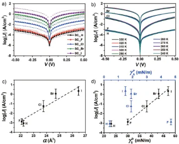
Figure 3a shows the log-average values of J (<log|J|>) vs the
applied bias V (the error bars are the log-standard deviations).
This Figure shows that the J(V) curves for junctions with X = H
or F are indistinguishable. In contrast, when X changes from F
(or H) to I, the values of <log|J|> increase by a factor of 3 (i.e., J
increases by three orders of magnitude). Below we discuss this observation in more detail.
To examine the mechanism of charge transport across the
junctions in more detail, we performed the J(V) measurements
as a function of temperature over the range of temperatures of 240 to 330 K using junctions where the EGaIn is mechanically stabilized in a through-hole in poly(dimethylsiloxane) (PDMS); the fabrication and characterization of these junctions are
described elsewhere.[40] Figure 3b shows that the J(V) curves
are independent of the temperature. From this observation, we conclude that in all cases the mechanism of charge transport across the junctions is coherent tunneling.
Figure 3c,d shows plots of <log|J|> determined at +0.50 V
(<log|J|>+0.50 V) as a function of α, γsD and γsP. We found that
the values of <log|J|>+0.50 V follow a surprisingly good linear
correlation with α and γsD, but no obvious correlation is
vis-ible with γsP or the permanent dipole moment of the molecules
normal to surface µ⊥(estimated from DFT; see page S25 and
Figure S17, Supporting Information). These results suggest that
the increase in the tunneling rates is primarily related to γsD
and α (which are related to each other).[39,41,42] To confirm this
COMMUNICA
TION
hypothesis, we also determined the values of <log|J|> for
junc-tions with other terminal groups (X = OH, COOH, NO2, CN,
or NH2; Figure S17, Supporting Information). In agreement
with findings by Whitesides and co-workers[9–11] these groups
changed the tunneling rates only within 1 order of magnitude though they span a large range of dipole moments (Table S2, Supporting Information). We note that these dipole moments were estimated from gas phase single molecules and not from
the SAMs. Zojer et al.[38] showed theoretically that the dipole
moment of SAMs depend on various factors, e.g., depolariza-tion effects (which are expected to be small in our study as we used aliphatic molecules), orientation of the molecules, or sur-face coverages, but here we solely wish to point out that for the
series of junctions with X = OH, COOH, NO2, CN, and NH2, J
did not change much as opposed to junctions with halogens. To investigate the mechanism of charge transport in more detail, we characterized the junctions by impedance spectros-copy (IS) because IS measures the dielectric properties of a medium as a function of frequency and makes it possible to
measure the contact resistance (RC in mΩ cm2), resistance of
the SAM (RSAM in Ω cm2), and C
SAM (in µF cm−2), independent
from each other.[43] The junctions were probed in the frequency
range of 100 Hz to 1 MHz using a sinusoidal signal with an amplitude of 30 mV following previously reported procedures (Figure S18, Supporting Information shows the Nyquist and
Bode plots).[44] The linearity of the system was confirmed by
Kramers–Kronig (KK) tests (Figure S19 and S20, Supporting Information). The data were fitted to the equivalent circuit
shown in Figure 1. The equivalent circuit consists of a constant
phase element (CPE) in parallel with RSAM both in series with
RC. We used a CPE instead of a pure capacitor to model CSAM
because the former represents an imperfect capacitor caused by defects in the electrode materials (e.g., grain boundaries,
step-edges, dislocations, etc.).[45,46] Although the fitting results are
very similar, the fitting errors (χ2fit) are reduced by a factor of
2–3 and are similar to the error of the KK-test χ2KK (see Table2
and Table S5, Supporting Information).
As we have shown before, in our junctions the RC is
domi-nated by the SAM//GaOx interface (the 0.7 nm thick GaOx layer
is about two orders of magnitude less resistive than the contact
resistance).[43] Therefore, we approximated the two interface
resistances as a single resistor RC.
www.advmat.de
www.MaterialsViews.com
Figure 3. a) Plots of <log|J|> against V for junctions with X = H, F, Cl, Br, and I. b) The J(V) measurements as a function of temperature ranging from 240 to 330 K for junctions with X = H, F, Cl, Br, and I. c) The values of <log|J|>+0.50 V as a function of α. d) The values of <log|J|>+0.50 V as a function of
γsD (black squares) and γsP (blue triangles). The dashed lines are guides to the eye and the error bars represent one log-standard deviation.
Table 2. Summary of the results of the IS measurements.
SAMsa) R C
[mΩ cm2]
RSAM
[Ω cm2]
CSAM
[µF cm−2]
εrb) dvdWc)
[Å] SC11H 6.8 ± 0.6 (3.4 ± 0.6) × 102 1.54 ± 0.07 2.93 ± 0.09 2.72
SC11F 7.0 ± 0.1 (4.9 ± 0.6) × 102 1.16 ± 0.02 2.00 ± 0.03 2.99
SC11Cl 4.7 ± 0.8 (4.6 ± 1.0) × 101 1.67 ± 0.02 2.96 ± 0.03 3.27
SC11Br 3.7 ± 0.2 (1.5 ± 0.1) × 100 2.6 ± 0.1 4.6 ± 0.2 3.37
SC11I 2.1 ± 0.3 (1.6 ± 0.3) × 10−1 4.4 ± 0.4 7.9 ± 0.7 3.50 a)The error bars represent the standard deviation of three independent
meas-urements; b)ε
r was determined from the CSAM values and using the Equation 2; c)d
COMMUNICA
TION
We note that, in principle, any junction—regardless whether it is classical or non-classical—can be fitted with an equivalent
circuit (as is common practice to model artificial atoms[47] for
instance). The equivalent circuit given in Figure 1 represents a SAM-based tunneling junction and we explain the physical meaning of the elements using a single tunneling barrier model, which includes contact resistance, in the framework
of the Landauer model given by Equation 3.[48] This analysis
makes it possible to define the contact and SAM resistance clearly (see for details ref. [44]). Here, the contact resistance is associated with the coupling of the molecules to the electrodes which is, in an ideal case, the inverse of the quantum
conduct-ance G0= 2e2/h (for M= 1) where h= Planck’s constant, e =
the charge of an electron, T= the transmission probability, and
M = the number of conduction channels.[48] The value of T
depends on both the molecule–electrode binding energy and the tunneling barrier height.
2 2
1
junction 2 2 C SAM
R h
e M h e M
T
T R R
= + − = + (3)
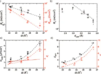
Figure 4a shows that the value of RC (7.0–2.1 mΩ cm2)
decreases with increasing α. One would expect the value
of resistance of the SAM top contact (RC,t) to increase with
increasing dvdW (estimated from the sums of the
respec-tive vdW radii, Table 2),[49] however, Figure 4b shows that R
C
decreases with increasing dvdW. It is well known that the Debye
(dipole-induced dipole) and London (induced dipole-induced
dipole) forces increase with increasing α (page S39 in the
Supporting Information). The changes of µ of the molecules
are small and do not follow an obvious correlation with RC,t
(Figure S21, Supporting Information). CA measurements
indi-cate that value of γsP (γsP= 32.4 mN m−1 and is similar in value
to γsD= 42.5 mN m−1) of the top electrode is large and
there-fore the permanent dipole associated with the GaOx layer may be important (Table S1, Supporting Information). Therefore we believe that with the increase of the polarizability of X, the vdW force between the top-electrode and SAM increases, which lowers the contact resistance.
Figure 4a shows that RSAM decreases from 490 to 0.16 Ω cm2
when X changes changed from F to I. This result shows that
the three orders of magnitude increase of J, observed in the
DC measurements (Figure 3), is mainly caused by a decrease
of the RSAM (and not by the change in RC because RC<< RSAM).
The substantial change in RSAM cannot be attributed to a
change in dSAM or ΓSAM as these parameters did not vary
sig-nificantly as a function of X. However, DFT (to obtain the projected density of state PDOS; page S27 in the Supporting Information) and TD-DFT (to obtain an approximation of the
HOMO–LUMO gap Eg; page S28–S29 in the Supporting
Infor-mation) calculations qualitatively justify this trend in RSAM as
Eg for the single molecule in gas phase decreases consistently
from C11F (Eg= 6.31 eV) to C11I (Eg= 4.70 eV). As described
earlier, the UPS data indicated that the energy level align-ment did not change with changing X (Table 1) and UV–vis measurements (page S29–S30 in the Supporting Information)
allowed us to estimate the optical Eg experimentally (we note
that UV–vis likely underestimates Eg as is explained in detail
in for example ref. [50]).[50] The DFT, TD-DFT, and UV–vis data
qualitatively agree and Table 1 shows that the LUMO levels
decrease with increasing Z. Since the LUMO levels are closer
to the Fermi levels than the HOMO levels, the mechanism of
COMMUNICA
TION
charge transport involves electron tunneling[51,52] and hence the
increase in tunneling rates is primarily caused by a decrease in the LUMO levels. We note that the shifts in the energy levels may be considerably larger once the SAMs are contacted by
the top-electrode than those estimated by UPS.[53] As explained
above, a decrease in the values of RC implies an increase in the
molecule–electrode interaction, which would also result in an
increase of T. Thus our data indicate that the large increase in
the values of J is the result of a combination of an increase in
the molecule–top electrode coupling and lowering of the tun-neling barrier height as the molecule–top electrode interaction increases with increasing polarizability of the terminal atom of the SAM.
Figure 4c shows the values of CSAM and εr plotted as a
func-tion of α. Here εr was determined using Equation 2 from the
experimentally obtained CSAM. We found that for junctions with
X = I, CSAM= 4.4 ± 0.4 µF cm−2 and εr= 7.9 ± 0.7, which are
both about four times higher than for junctions with X = F.[43]
The solid line in Figure 4c represents a fit to the Clausius–
Mosotti relation, which correlates εr with α, but ignores bulk
effects.[54,55]
As expected, the Clausius–Mosotti relation does not fit our
data well, but the εDFT values calculated by the van der Waals
DFT-D2 method are in close agreement with our experimental results, as shown in Figure 4d (the off-set between theory and experiment may be attributed to the simplicity of the model as the effects of the electrode and the thiol group, or
depolariza-tion effects[22,38,56,57] were ignored). The details of the model
and calculation are described on page S26 in the Supporting Information. Our calculations qualitatively agree well with the
calculations reported by Ratner and co-workers.[24] They showed
theoretically an increase by a factor of 1.7 in εr from 5.1 to 8.7
for monolayers of trans-polyacetylene by changing the halogen
termini of these SAMs from F to I (who also ignored the elec-trodes and the thiol anchoring group). These authors also
showed that εr of conjugated SAMs is less sensitive to the
pres-ence of highly polarizable atoms than non-conjugated SAMs,
which explains why we observed a factor of 4 increase of εr. This
notion also explains why Yoon et al. only observed marginal effects in the tunneling rates in EGaIn junctions of the form
AgTS–S(CH
2)n(p-C6H5X)//GaOx/EGaIn with n = 0 or 1 and
X = H, F, Cl, Br, and I (these authors did not measure εr).[58] In
addition, these short and conjugated SAMs hybridize strongly
with the bottom-electrode masking molecular effects.[59]
In conclusion, our experiments show that in tunneling
junc-tions of the form AgA-TS–SC
11X//GaOx/EGaIn the tunneling
rate increases by three orders of magnitude and the dielec-tric constant increases from 2 to 8 when the polarizability of
X increases (where X = H, F, Br, Cl, or I). These results show
that it is possible to tune the dielectric constant by controlling
the polarizability via high Z substituents, which in turn also
make it possible to control the HOMO–LUMO gaps and con-sequently the tunneling rates across the SAM-based junctions.
The halogenated SAMs have high capacitances (CSAM =
4.4 ± 0.4 µF cm−2 when X = I), but the leakage currents (i.e.,
the tunneling current across the junctions) increased with increasing capacitance. Although in this study we kept the SAM thickness the same, our results imply that it is possible to engineer the dielectric response of SAMs at the atomic level,
which are needed in optimizing the balance between the dielec-tric response and the leakage current.
Supporting Information
Supporting Information is available from the Wiley Online Library or from the author.
Acknowledgements
D.W. and D.F. contributed equally to this work. The authors acknowledge the National Research Foundation (NRF) for supporting this research under the Competitive Research Programme (CRP) Award No. NRF-CRP8-2011-07. This research was supported by the National Research Foundation, Prime Minister’s Office, Singapore under its Medium sized centre programme. C.A.N. acknowledges the Ministry of Education for financial support (MOE R-144-000-325-112). The authors thank Dr Xiao-Jiang Yu for help at the Singapore Synchrotron Light Source (SSLS). R. M. Metzger, M. E. Michel-Beyerle, J. R. Miller, M. D. Newton, D. R. Rolison, O. Sankey, K. S. Schanze, J. Yardley, X. Zhu, J. Phys. M. Baghbanzadeh, F. C. Simeone, G. M. Whitesides, Nano Lett. 2014, 14, 3521.
[12] M. M. Thuo, W. F. Reus, C. A. Nijhuis, J. R. Barber, C. Kim, M. D. Schulz, G. M. Whitesides, J. Am. Chem. Soc.2011, 133, 2962. [13] T. Toledano, H. Sazan, S. Mukhopadhyay, H. Alon, K. Lerman,
T. Bendikov, D. T. Major, C. N. Sukenik, A. Vilan, D. Cahen, Lang-muir2014, 30, 13596.
[14] N. Nerngchamnong, L. Yuan, D.-C. Qi, J. Li, D. Thompson, C. A. Nijhuis, Nat. Nanotechnol.2013, 8, 113.
[15] D. Fracasso, M. I. Muglali, M. Rohwerder, A. Terfort, R. C. Chiechi,
J. Phys. Chem. C2013, 117, 11367.
[19] D. Fracasso, H. Valkenier, J. C. Hummelen, G. C. Solomon, R. C. Chiechi, J. Am. Chem. Soc.2011, 133, 9556.
www.advmat.de
COMMUNICA
TION
[20] C. M. Guedon, H. Valkenier, T. Markussen, K. S. Thygesen, J. C. Hummelen, S. J. van der Molen, Nat. Nano2012, 7, 305. [21] B. Kim, S. H. Choi, X. Y. Zhu, C. D. Frisbie, J. Am. Chem. Soc.2011,
133, 19864.
[22] L. Romaner, G. Heimel, C. Ambrosch-Draxl, E. Zojer, Adv. Funct. Mater.2008, 18, 3999.
[23] V. Obersteiner, D. A. Egger, G. Heimel, E. Zojer, J. Phys. Chem. C 2014, 118, 22395.
[24] H. M. Heitzer, T. J. Marks, M. A. Ratner, ACS Nano2014, 8, 12587. [25] T. Toledano, A. Biller, T. Bendikov, H. Cohen, A. Vilan, D. Cahen, J.
Phys. Chem. C2012, 116, 11434. [26] C. Groves, Nat. Mater.2013, 12, 597.
[27] R. P. Ortiz, A. Facchetti, T. J. Marks, Chem. Rev.2010, 110, 205. [28] J. C. Love, L. A. Estroff, J. K. Kriebel, R. G. Nuzzo, G. M. Whitesides,
Chem. Rev.2005, 105, 1103.
[29] M. Halik, H. Klauk, U. Zschieschang, G. Schmid, C. Dehm, M. Schutz, S. Maisch, F. Effenberger, M. Brunnbauer, F. Stellacci,
Nature2004, 431, 963.
[30] R. C. Chiechi, E. A. Weiss, M. D. Dickey, G. M. Whitesides, Angew. Chem., Int. Ed.2008, 47, 142.
[31] W. F. Reus, C. A. Nijhuis, J. R. Barber, M. M. Thuo, S. Tricard, G. M. Whitesides, J. Phys. Chem. C2012, 116, 6714.
[32] L. Yuan, L. Jiang, B. Zhang, C. A. Nijhuis, Angew. Chem., Int. Ed. 2014, 53, 3377.
[33] J. B. Schlenoff, M. Li, H. Ly, J. Am. Chem. Soc.1995, 117, 12528. [34] B. de Boer, A. Hadipour, M. M. Mandoc, T. van Woudenbergh,
P. W. M. Blom, Adv. Mater.2005, 17, 621.
[35] A.-E. Haj-Yahia, O. Yaffe, T. Bendikov, H. Cohen, Y. Feldman, A. Vilan, D. Cahen, Adv. Mater.2013, 25, 702.
[36] A. Natan, L. Kronik, H. Haick, R. T. Tung, Adv. Mater. 2007, 19, 4103.
[37] G. Heimel, L. Romaner, J.-L. Brédas, E. Zojer, Phys. Rev. Lett.2006,
96, 196806.
[38] L. Wang, G. M. Rangger, L. Romaner, G. Heimel, T. Bucˇko, Z. Ma, Q. Li, Z. Shuai, E. Zojer, Adv. Funct. Mater.2009, 19, 3766.
[39] F. M. Fowkes, Ind. Eng. Chem. Res.1964, 56, 40.
[40] A. Wan, L. Jiang, C. S. S. Sangeeth, C. A. Nijhuis, Adv. Funct. Mater. 2014, 24, 4442.
[41] H. Margenau, Rev. Mod. Phys.1939, 11, 1.
[42] H. Y. Erbil, Surface Chemistry: Of Solid and Liquid Interfaces, Black-well Publishing Ltd., Oxford, UK 2006.
[43] C. S. S. Sangeeth, A. Wan, C. A. Nijhuis, J. Am. Chem. Soc.2014,
136, 11134.
[44] C. S. Suchand Sangeeth, A. Wan, C. A. Nijhuis, Nanoscale2015, 7, 12061.
[45] J.-B. Jorcin, M. E. Orazem, N. Pébère, B. Tribollet, Electrochim. Acta 2006, 51, 1473.
[46] M. E. Orazem, B. Tribollet, Electrochemical Impedance Spectroscopy, John Wiley & Sons, Inc., Hoboken, NJ, USA 2008.
[47] W. G. van der Wiel, S. De Franceschi, J. M. Elzerman, T. Fujisawa, S. Tarucha, L. P. Kouwenhoven, Rev. Mod. Phys.2002, 75, 1. [48] S. Datta, Electronic Transport in Mesoscopic Systems, Cambridge
University Press, Cambridge, UK 1995.
[49] K. E. Riley, K. M. Merz, J. Phys. Chem. A2007, 111, 1688. [50] J.-L. Bredas, Mater. Horiz.2014, 1, 17.
[51] K. Smaali, N. Clément, G. Patriarche, D. Vuillaume, ACS Nano 2012, 6, 4639.
[52] Y. Qi, O. Yaffe, E. Tirosh, A. Vilan, D. Cahen, A. Kahn, Chem. Phys. Lett.2011, 511, 344.
[53] K. Moth-Poulsen, T. Bjornholm, Nat. Nanotechnol.2009, 4, 551. [54] A. Natan, N. Kuritz, L. Kronik, Adv. Funct. Mater.2010, 20, 2077. [55] A. R. Blythe, D. Bloor, Electrical Properties of Polymers, 2nd ed.,
Cam-bridge University Press, CamCam-bridge, UK 2005.
[56] D. Cornil, Y. Olivier, V. Geskin, J. Cornil, Adv. Funct. Mater.2007, 17, 1143.
[57] M. L. Sushko, A. L. Shluger, Adv. Funct. Mater.2008, 18, 2228. [58] G. D. Kong, M. Kim, H.-J. Jang, K.-C. Liao, H. J. Yoon, Phys. Chem.
Chem. Phys.2015, 17, 13804.
[59] L. Yuan, N. Nerngchamnong, L. Cao, H. Hamoudi, E. del Barco, M. Roemer, R. K. Sriramula, D. Thompson, C. A. Nijhuis, Nat. Commun.2015, 6, 6324, DOI:10.1038/ncomms7324.