Available online at http://journal.walisongo.ac.id/index.php/jnsmr
Effect of Growth Pressure on Structural Properties of SiC Film Grown on
Insulator by Utilizing Graphene as a Buffer Layer
Budi Astuti1, Shaharin Fadzli Abd Rahman2, Masahiro Tanikawa3,
Mohamad Rusop Mahmood4 , Kanji Yasui3 & Abdul Manaf Hashim5
1Physics Department, Faculty of Mathematics and Natural Science, Universitas Negeri Semarang, Central Java,Indonesia
2Faculty of Electrical Engineering, Universiti Teknologi Malaysia, 81310 Skudai, Johor, Malaysia
3Department of Electrical Engineering, Nagaoka University of Technology, 1603-1 Kamitomioka-cho, Nagaoka, Niigata 940-2188, Japan
4Faculty of Electrical Engineering, Universiti Teknologi MARA, 40450 Shah Alam, Selangor, Malaysia
5Malaysia-Japan International Institute of Technology, Universiti Teknologi Malaysia, 54100 Kuala Lumpur, Malaysia
Corresponding author:
Recived: 10 May 2015, Revised : 28 May 2015 Accepted: 23 June 2015.
Abstracts
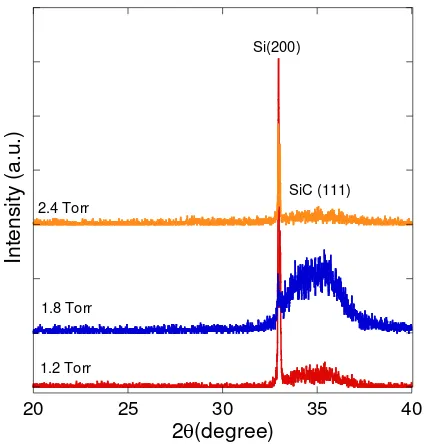
Heteroepitaxial growth of silicon carbide (SiC) on graphene/SiO2/Si substrates was carried out using a home-made hot-mesh chemical vapor deposition (HM-CVD) apparatus. Monomethylsilane (MMS) was used as single source gas while hydrogen (H2) as carrier gas. The substrate temperature, tungsten mesh temperature, H2 flow rate and distance between mesh and substrate were fixed at 750 °C, 1700 °C, 100 sccm and 30 mm, respectively. The growth pressures were set to 1.2, 1.8 and 2.4 Torr. The growth of 3C-SiC (111) on graphene/SiO2/Si were confirmed by the observation of θ- θ diffraction peak at . 8. The diffraction peak of thin film on graphene/SiO2/Si substrate at pressure growth is 1.8 Torr is relatively more intense and sharper than thin film grown at pressure growth 1.2 and 2.4 Torr, thus indicates that the quality of grown film at 1.8 Torr is better. The sharp and strong peak at 33 was observed on the all film grown, that peak was attributed Si(200) nanocrystal. The reason why Si (200) nanocrystal layer is formed is not understood. In principle, it can’t be denied that the low quality of the grown thin film is influenced by the capability of our home-made apparatus. However, we believe that the quality can be further increased by the improvement of apparatus design. As a conclusion, the growth pressures around 1.8 Torr seems to be the best pressures for the growth of heteroepitaxial 3C-SiC thin film.
1.
Introduction
Growth of SiC/c-Si heteroepitaxial are interesting topic on the point of view the potential application of SiC material on the production of heterobipolar transistor [1] or optoelectronic devices [2]. Hydrogenated amorphous silicon carbide is preferred to use in many studies in comparison with monocrystalline material, since the growth temperature is relatively low and which guarantees a large compatibility among the fabrication processes of the silicon carbide layer with current silicon technology. In order to improve the performance of the devices, carrier mobility should be enhanced and this is possible with the crystallization of SiC layers. Hence, it is important to grow heteroepitaxial crystalline SiC on different substrates.
Growth of the Single crystalline SiC films is usually realized only at high growth temperature greater than 1000 C [3]. owing to the lattice mismatch (20%) and the difference in the thermal expansion coefficient (8%) between SiC and Si, it is quite likely generating a residual stress and a high density of interface defects when the processing temperatures are very high [4]. However, several applications can benefit from heteroepitaxial system. Heteroepitaxial SiC/c-Si with optimized properties possesses potential application such as on switching devices [5], sensors [6], detectors [7] and micro-electrical mechanical system (MEMS) [8].
Graphene is one monolayer of carbon atoms packed into a two-dimensional (2D) honeycomb crystal lattice. The electron in an ideal graphene sheet behaves like massless Dirac-Fermion. Graphene possesses high carrier mobility, up to 200,000 cm2/Vs, even at room distance without scattering. This makes it superior for transport properties and the material itself is very robust, highly elastic and
chemically inert offering a high potential for technological application [10].
In order to realize high quality SiC thin film on silicon, we have studied the growth of SiC on Si substrate by using carbonization layer to reduce the lattice mismatch between SiC and Si interfaces [11]. The latter work triggers and idea to employ graphene , a 2D carbon material with only one atomic-layer thick, as a buffer layer for epitaxial growth of SiC thin film on insulator substrate. To our knowledge, growth of the material on the insulator substrate is not new topic, such as Ge-on-insulator[12], graphene-on-insulator[13], GaAs-on-insulator [14] and SiC-on-insulator [15]. However, the growth SiC on insulator by introducing graphene as buffer layer has not been reported yet. In this pioneer work, we reported the effect of the pressure and graphene as a buffer layer for heteroepitaxial growth of SiC thin film.
2.
Experiments Procedure
crystalline sizes were determined from the full width at half maximum (FWHM) of XRD peaks using Scherrer’s formula. Cross sectional image of the SiC film were observed using field effect scanning electron microscope (FESEM). Raman scattering spectra were measured using micro-raman equipment (Jobin Yvon, Horiba) with Ar+ laser 514.5 nm wavelength.
TMP
RP Exhaust
MMS H2 N2
W-mesh wire
Substrate PBN
heater
Figure 1. Schematic of the homemade hot-mesh CVD apparatus.
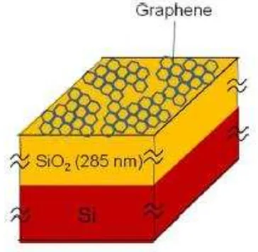
Figure 2. Schematic of graphene/SiO2/Si(100) substrate (eye bird view)
3.
Result and Discussion
The FESEM image of as received graphene/SiO2/Si(100) substrate from Graphene Laboratories Inc. USA is shown in Fig.
3. It is clear that the size of grapheme grains of several tens micrometer in the diameter. The polycrystalline graphene grains were grown by CVD technique with the coverage of single layer graphene grains of 90%. The thickness of the graphene grain was also confirmed by Raman measurement, as showns in Fig. 4. Based on the Fig. 4, the sharp peak was clearly observed at 1580 cm-1 and 2670 cm-1 is attributed to G and 2D bands, respectively. The ratio intensity of the 2D and G band (I2D/IG) is about 1.6, hence indicate that the graphene is a single layer [16].
Figure 3. FESEM image as-received graphene/SiO2/Si(100) substrate
of (111) oriented SiC on graphene in <111> direction is feasible (Fig. 5).
0
1000 1500 2000 2500 3000 3500
In graphene/SiO2/Si(100) substrate at growth pressure 1.2, 1.8, and 2.4 Torr.
Fig. 5 shows the X-ray diffraction (XRD) spectra of the samples deposited on the graphene/SiO2/Si(100) substrate at various gas
pressure. Two diffraction peak were found in the range from 20 to 40. The peaks at 33 is attributed to crystalline Si(200) peak [18]. Komura et. al. [19] was reported the film grown at below 1.5 Torr is contained Si nanocrystallites, where that Si nanocrystallite embedded amorphous SiC (a-SiC) film were prepared by HWCVD using CH4 as a carbon source [20] and our result at the low pressure condition below 1.5 Torr are consistent with it. On the other hand, for films prepared at 1.8 introducing graphene as buffer layer. According to this result, we speculate that the growth of 3C-SiC on graphene/SiO2/Si(100) substrate has been enhance in (111) domain. In this work, the grown SiC films were also polycrystalline same as the reported SiC film on SiO2 [22-24] since the polycrystalline single layer graphene flake were used. However, if the technology to form large area single crystalline grapheme is realized and then, such single crystalline grapheme structures is applied, it should lead to the realization of highly oriented single crystalline 3C-SiC (111) continous thin film. It seem to show that grapheme is a promising buffer layer to grow single crystalline material structure on amorphous material. Recently, Takahashi et al. reported the graphitization process or the formation of epitaxial grapheme on the 3C-SiC (111) surface by annealing process in ultrahigh vacuum condition [25]. Therefore, it supports the feasibility of forming 3C-SiC film on graphene since both process are simply reversed to each other and we assume that the same bonding structures should be formed.
formed at the interface between SiC and SiO2. Fig. 6 shows the cross sectional FESEM of the 3C-SiC film on graphene/SiO2/Si(100) substrate. It is clearly shown that 3C-SiC film can be grown on the surface of the insulator which is the polycrystalline grapheme as a buffer layer is incorporation on the SiC film formation. The thickness of the 3C-SiC film is about 2 µm where the film shows grain like structure which is the size of the grain are similar to the size of graphene grain.
Figure 6. Cross sectional FESEM image of 3C-SiC film grown on grapheme/SiO2/Si(100) substrate.
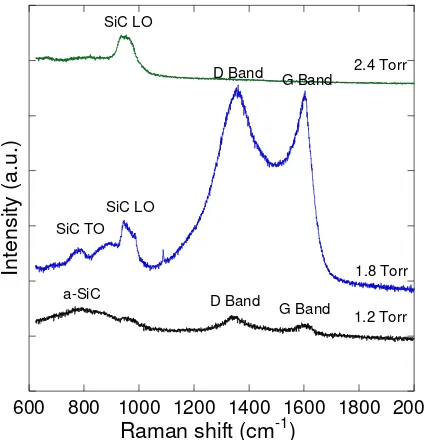
The Raman scattering spectra of the 3C-SiC film on graphene/SiO2/Si(100) substrate prepared at variation of the pressure growth is shown in Fig. 7. It is reported that SiC gives Raman scattering from a transverse optic (TO) phonon at approximately 796 cm-1 and a longitudinal optic phonon (LO) at 973 cm-1 for bulk crystal 3C-SiC [26]. In this work, the TO and LO peaks of SiC crystallites is shifted toward a lower wavenumber region (redshift) and broadened with respect to those of the bulk 3C-SiC. Broad and low intensity of the TO and LO phonon mode peaks for SiC is indicated that the grown film is polycrystalline with small crystallite size [27-29]. The shifting of the TO and LO peaks is caused by the small crystallite size (quantum confinement effect) [30] and the defect of the structure which is strain associated with them [31]. Accordingly, we
concluded that the peaks at around 789 cm-1 and 955 cm-1 would be due to TO and LO modes of 3C-SiC, respectively. As shown in Fig. 6 the intensities of the Raman peaks due to LO mode 3C-SiC increased with pressure growth, indicating that the crystallinity of 3C-SiC was improved.
600 800 1000 1200 1400 1600 1800 2000
In
te
nsi
ty
(a.u
.)
Raman shift (cm-1)
1.2 Torr 1.8 Torr 2.4 Torr
SiC TO SiC LO
D Band G Band SiC LO
a-SiC D Band
G Band
Figure 7. Raman spectra of grown SiC film on grapheme/SiO2/Si(100) substrate.
4.
Conclusion
In conclusion, these preliminary result suggest that graphene can be used as a promising buffer layer for growth of 3C-SiC thin films on insulator at relatively low temperature. Based on the XRD and Raman result, the 3C-SiC film was ontained is polycrystalline 3C-SiC with (111) domain orientation. The growth pressure around 1.8 Torr seems to be the best pressure for the growth of heteroepitaxial 3C-SiC thin films.
Acknowledgment
References
Optoelectronics, 1 (1968) 67.
[3] S. Miyajima, A. Yamada, and M. Konagai,
Jpn. J. Appl. Phys. 46 (2007) 1415.
[4] Q. Cheng, S. Xu, J. Long, and K. Ostrikov,
Chem. Vap. Deposition, 13 (2007) 561.
[5] S.S. Sheng, M.G. Spencer, X. Tang, P. Zhou, Kuznetsov, A.A. Lebedev, Appl. Surface Sci.
184 (2001) 455.
[8] C. Ricciardi, E. Bennici, M. Cocuzza, P. Mandracci, D. Bich, V. Guglielmetti, G. Barucca, Thin Solid Films, 427 (2003) 178. [9] K.I. Bolotin, K. J. Sikes, Z. Jiang, M. Klima, G. Akahane, Thin Solid Films, 516 (2008) 644. [16] W. Choi, I. Lahiri, R. Seelabayina, and Y.S. S. Nitta. Thin Solid Films. 395 (2001) 240. [21] S. Ulrich, T. Theel. J. Schwan, V. Batori, M.
Scheib, and H. Ehrhardt, Diamond. Relat. Mat. 6 (1997) 645.
[22] C.H. Wu, C.A. Zorman, M. Mehregany, Mat.
Sci. Forum, 541 (2000) 338-342.
[23] Y.M. Zhao, G.S. Sun, J. Ning, X.F. Liu, W.S. V. Osipov, N. A. Feoktistov, S. A. Grudinkin,