Effects of dielectric material and linewidth on thermal stresses of Cu line structures
Dongwen Gan1, Guotao Wang1 and Paul S. Ho1
1Laboratory for Interconnect and Packaging, University of Texas at Austin, Austin, TX 78712-1063
Xiaorong Morrow2 and Jihpern g Leu2
2Components Research, Intel Corporation, M/S: RA1-204, 5200 N.E. Elam Young Parkway Hillsboro, OR 97214
Abstract
Thermal stresses of Cu line structures of 0.4 and 0.2 µm linewidth integrated with fluorinated silicon oxide SiOF and two kinds of low k dielectrics, carbon doped oxide CDO and organic polymer SiLKTM were measured using x-ray diffraction method. Finite element analysis was performed to evaluate the stress behavior of the Cu lines to examine the effect of scaling in linewidth. After verification with the measured Cu line stresses, FEA was extended to evaluate the stress behavior of the low k dielectrics. The confinement effects on thermal stresses due to low k dielectric on Cu lines and Cu lines on the dielectric are compared and discussed.
Introduction
Structural integrity of copper interconnects integrated with low dielectric constant (k) materials is a major reliability concern. Compared to SiO2, low k interlevel dielectrics (ILD) are significantly softer and expand more during thermal processing. Thermal stress behavior of Cu/low k damascene line structures has been measured using x-ray diffraction method (1,2). The barrier and the cap layer were found to play an important role in confining thermal deformation of Cu lines, resulting in a stress state distinctly different from that of Alco/low k lines not embedded in the damascene structure (3). These studies raise two basic questions concerning thermal stress behavior of Cu/low k damascene structures. First, what is the effect of the dielectric material, particularly when the linewidth reduces below 0.25 µm. The second question concerns the deformation and stress characteristics of the low k ILD. The stress behavior of the ILD in the confined sub micron geometry of the damascene structure is expected to be quite different from that measured on blanket films or large pad structures. So far there exists little such information to evaluate the structural reliability of the low k material.
In this paper, we investigate these two questions. To study the effect of ILD material, thermal stresses were measured on Cu damascene line structures of 0.4 and 0.2 µm linewidths integrated with SiOF, carbon doped oxide CDO and SILKTM using x-ray diffraction method. Finite element analysis (FEA) was performed to evaluate the stress behavior of the Cu lines to examine the effect of scaling in linewidth. After verification with the measured Cu line stresses, FEA was extended to evaluate the stress behavior of the low k dielectrics. The elastic moduli of the three ILD extend from 72GPa for SiOF, 4.47GPa for CDO, and 2.45GPa for SiLKTM, providing a wide range of mechanical property for this study.
Experimental Details
X-ray diffraction method was used to measure the thermal stresses in Cu damascene line structures. Details of the method and stress analysis can be found elsewhere (4,5). In this study, (311) plane spacing was measured in different
inclination angle (ψ) to the surface normal and rotation angle (φ), then linear relation between d and sin2ψ was used to determine the three principal strains. The line coordination is defined to be x direction along the line, y across the line and z normal to the line. All measurements in this study were performed in-situ for two thermal cycles to 400°C at a ramp rate of 2°C/min. The purpose of the first thermal cycle is to eliminate any long-term stress relaxation effect, therefore, only results from the second cycle are presented here.
The samples contained parallel damascene lines designed specifically for x-ray measurements and two sets of line width/pitch (0.4/0.4 and 0.2/0.2 µm) were measured. Test structures were fabricated using damascene processing with 0.35 µm trench depth, a 105nm Si3N4 cap layer and Ta barriers of 5 nm average thickness in the trench.
Finite element analysis
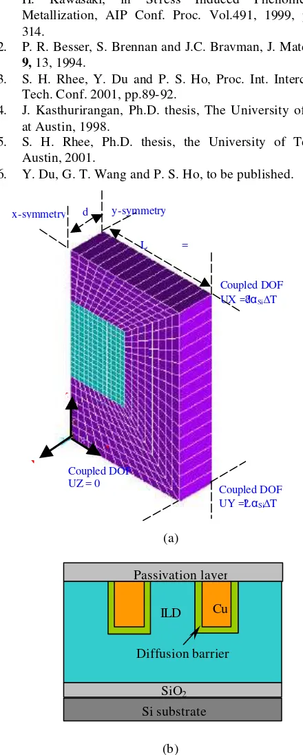
In this study, a 3D model containing multiple copper lines was first developed using the ABAQUS program. A good convergence was found in the calculation when the number of lines approaching 20. Then sub-modeling technique was used to develop simplified line models in order to save computation time. For periodic line structures, a sub-model containing only half of the periodic line structure was built. Various boundary conditions were applied and compared with the multi-line model. We found that by choosing suitable boundary conditions, the half-line model can obtain the same results as the multi-line model. Details of model development and verification are described elsewhere (6). In Fig.1, we show the sub-model together with a schematic cross-section of the test structure. The material properties used in FEA are summarized in Table 1.
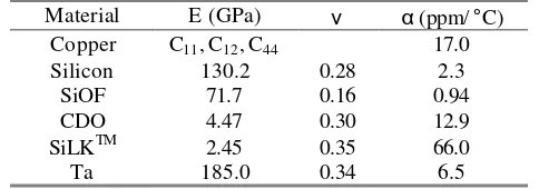
Table 1 Mechanical properties of the related materials at 25°C Material E (GPa) ν α (ppm/°C)
Copper C11, C12, C44 17.0
Silicon 130.2 0.28 2.3
SiOF 71.7 0.16 0.94
CDO 4.47 0.30 12.9
SiLKTM 2.45 0.35 66.0
Ta 185.0 0.34 6.5
Results and discussions
thermomechanical properties. The stress behavior of the 0.2
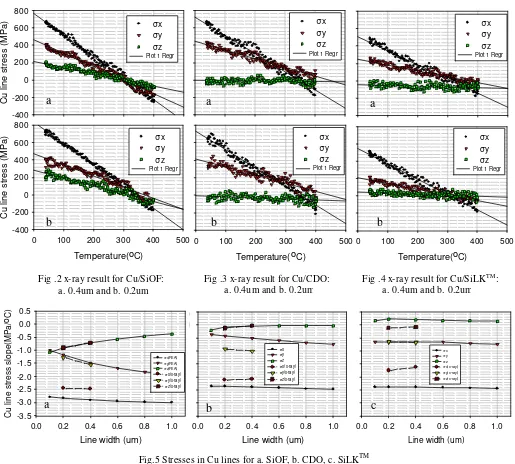
µm lines evolves in a similar manner with slightly higher σx and σz and lower σy. This reflects an increasing confinement effect on the Cu lines as the linewidth decreases. Thermal stresses obtained for Cu/CDO lines are shown in Figs.3a and b for 0.4 and 0.2 mm lineswidths respectively and in Figs.4a and 4b for Cu/ SiLKTM lines respectively. Compared to SiOF, CDO is weaker by about 16x in elastic modulus but expands more than 13x. This causes a decrease in dielectric confinement for Cu lines as reflected in the stress behavior in that σx and σz in Cu/CDO lines are reduced with σz reducing to almost zero. This trend continues for SiLKTM, which is even softer and expands more than CDO. For example, σx in SiLKTM structures is reduced to below 500MPa at the end of the thermal cycle.
Results from FEA for SiOF line structures are shown in Fig.5a as a function of linewidth. In comparison with stress data, we plot only the slopes of stress vs. temperature since all stress components vary linearly with temperature. With decreasing linewidth, the stress slope along the x direction decreases while increases along the y and z directions gradually. This reflects the increase in confinement across the line and normal to the line directions. For comparison, the measured stress slopes for 0.4 and 0.2 µm SiOF line structures are plotted also. There seems to be a good agreement between the measured and calculated stress slopes in all directions. The FEA results are plotted and compared with measured stress slopes in Fig.5b for CDO structures and in Fig.5c for SiLKTM structures respectively. It is interesting to note that the temperature slopes for these two low k dielectrics do not seem to vary much as linewidth decreases. This indicates that below 1µm linewidth, the confinement from ILD and barrier/cap layers on the Cu line does not vary much with decreasing linewidth. As we see later that the stresses in the ILD change considerably with linewidth, this means that the thermomechancal interaction between Cu and ILD does change. We conclude, therefore, the constant stress slopes with linewidth indicates that the contribution to stress confinement of Cu lines from these soft low k materials is relatively small compared with the contribution from the barrier and cap layers.
After verification, FEA was extended to calculate the stress behavior of the low k dielectrics. The results are presented as a function of linewidth in Figs. 6a, b and c for SiOF, CDO and SiLKTM respectively. The stresses plotted here represent the stress values obtained by averaging over the ILD cross section between the Cu lines. All the stress levels vary considerably with linewidth, suggesting that the Cu line and the barrier and cap layers form a “superstructures” confining the low k ILD. The confinement effect depends on the properties of the ILD and the line geometry. For strong material such as SiOF with a low CTE, the confinement induces stresses of opposite signs along y vs. x and z directions. For soft materials such as SiLKTM with a large CTE, the stress state becomes nearly hydrostatic with decreasing linewidth. Such a stress state is significantly different from that observed in SiOF structures. The implication on stress reliability of low k dielectrics has yet to be investigated.
Acknowledgment
This research was supported by the Semiconductor Research Corporation through the Center for Advanced Interconnect Science and Technology at RPI.
References
1. J. Kasthurirangan, Y. Du, P. Ho, C. Capasso, M. Gall, and H. Kawasaki, in St ress Induced Phenomena in Metallization, AIP Conf. Proc. Vol.491, 1999, pp.304-314.
2. P. R. Besser, S. Brennan and J.C. Bravman, J. Mater. Res. 9, 13, 1994.
3. S. H. Rhee, Y. Du and P. S. Ho, Proc. Int. Interconnect Tech. Conf. 2001, pp.89-92.
4. J. Kasthurirangan, Ph.D. thesis, The University of Texas at Austin, 1998.
5. S. H. Rhee, Ph.D. thesis, the University of Texas at Austin, 2001.
6. Y. Du, G. T. Wang and P. S. Ho, to be published.
(a)
(b)
Fig. 1 (a) Simple model for stress simulation and (b) cross-section of the testing structure
x-symmetry y-symmetry
Coupled DOF UX =??dαSi∆T
d
Coupled DOF UZ = 0
L =
X
Y Z
Coupled DOF UY =?LαSi∆T
Cu ILD
Passivation layer
Cu
SiO2
Si substrate Diffusion barrier
Cu line stress (MPa)
-400
Cu line stress (MPa)
-400
Fig.5 Stresses in Cu lines for a. SiOF, b. CDO, c. SiLKTM
Line width(um)
Fig.6 Stresses in the ILD between Cu lines. a. SiOF, b. CDO, c. SiLKTM Line width (um)
0.0 0.2 0.4 0.6 0.8 1.0
Cu line stress slope(MPa/