ANALOG AND DIGITAL
COMMUNICATION
Prepared according to Anna university syllabus R-201
7
(Common to III semester-CSE/IT )
G. E
lumalai
,
M.E.,(Ph.D)
Assistant Professor (Grade I)
Department of Electronics and Communication Engineering
Panimalar Engineering College
Chennai.
Er
. m. J
aiGanEsh
,
M.E.,
Assistant Professor
Department of Electronics and Communication Engineering
Panimalar Engineering College
Chennai.
SREE KAMALAMANI PUBLICATIONS
Publised by SREE KAMALAMANI PUBLICATIONS. New No. AJ. 21, old No. AJ. 52, Plot No. 2614, 4th Cross, 9th Main Road, Anna Nagar -600 040,
Chennai, Tamilnadu, India Landline: 91-044-42170813, Mobile: 91-9840795803
EMAilid: [email protected] 1ST EdiTioN 2014
2Nd REViSEd EdiTioN 2016
Copyright © 2014, by Sree Kamalamani Publications.
No part of this publication may be reproduced or distributed in any form or by any means, electronic, mechanical, photocopying, recording or otherwise or stored in a database or retrieval system without the prior written permission of the publishers.
This edition can be exported from India only by the Publishers, Sree Kamalamani Publications.
ISBN (13 digits): 978-93-85449-12-3
Typeset & Coverpage :
Sree Kamalamani PublicationS
New No. AJ. 21, Old No. AJ. 52, Plot No 2614, 9th Main, 4th cross, Anna Nagar-600 040
Chennai, Tamilnadu, India.
lANdliNE: 91-044-42170813, MobilE: 91-9840795803
G.Elumalai M.E., is working as an Assistant Professor (Grade – I) in the Department of Electronics and Communication Engineering, Panimalar Engineering College, Chennai. He obtained his B.E. in Electronics and Communication Engineering; M.E. in Applied Electronics and Ph.D pursing in Wireless Sensor Network. His areas of interests are Communication System, Digital communication, Digital signal processing and Wireless Sensor Network. He has more than 13 years of experience.
Dear Students,
We are extremely happy to present the book “Analog and Digital Communication” for you. This book has been written strictly as per the revised syllabus (R2013) of Anna University. We have divided the subject
into five units so that the topics can be arranged and understood proper -ly. The topics within the units have been arranged in a proper sequence
to ensure smooth flow of the subject.
Unit I - Introduce the basic concepts of communication, need of modulation and different types of analog modulation (Amplitude modu-lation, Frequency modulation and Phase modulation).
Unit II - Deals with basic concepts of digital communication which includes ASK, FSK, PSK, QPSK and QAM.
Unit III - Discuss about concept of data communication and various pulse modulation technique.
Unit IV - Concentrate on various techniques for error control cod-ing.
Unit V – Describe about multiuser radio communication.
A large number of solved university examples and university questions have been included in each unit, so we are sure that this book will cater all your needs for this subject.
We have made every possible effort to eliminate all the errors in
this book. However if you find any, please let we know, because that will
help for us to improve further.
G.Elumalai
M.Jaiganesh
UNIT I ANALOG COMMUNICATION
Noise: Source of Noise - External Noise- Internal Noise- Noise Calculation. Introduction to Communication Systems: Modulation – Types - Need for Modulation. Theory of Amplitude Modulation - Evolution and Description of SSB Techniques - Theory of Frequency and Phase Modulation – Comparison of various Analog Communication System (AM – FM – PM).
UNIT II DIGITAL COMMUNICATION
Amplitude Shift Keying (ASK) – Frequency Shift Keying (FSK) Minimum Shift Keying (MSK) –Phase Shift Keying (PSK) – BPSK – QPSK – 8 PSK – 16 PSK - Quadrature Amplitude Modulation (QAM) – 8 QAM – 16 QAM – Bandwidth Efficiency– Comparison of various Digital Communication System (ASK– FSK – PSK – QAM).
UNIT III DATA AND PULSE COMMUNICATION
Data Communication: History of Data Communication - Standards Organiza-tions for Data Communication- Data Communication Circuits - Data Communication Codes - Error Detection and Correction Techniques - Data communication Hardware - serial and parallel interfaces. Pulse Communication: Pulse Amplitude Modulation (PAM) –Pulse Time Modulation (PTM) – Pulse code Modulation (PCM) - Comparison of various Pulse Communication System (PAM – PTM – PCM).
UNIT IV SOURCE AND ERROR CONTROL CODING
Entropy, Source encoding theorem, Shannon fano coding, Huffman coding, mutual information, channel capacity, channel coding theorem, Error Control Coding, linear block codes, cyclic codes,
convolution codes, viterbi decoding algorithm.
UNIT V MULTI-USER RADIO COMMUNICATION
TABLE OF CONTENTS
UNIT – I ANALOG COMMUNICATION 1.1-1.120
1.1 Introduction 1.2
1.2 Noise 1.5
1.3 Introduction to communication system 1.12
1.4 Modulation 1.16
1.5 Need for modulation 1.17
1.6 Classifications of modulation 1.20
1.7 Some important definitions related to
communication 1.21
1.8 Theory of Amplitude modulation 1.24
1.9 Generation of SSB 1.58
1.10 AM – Transmitters 1.65
1.11 AM Super heterodyne receiver with its characteristic
Performance 1.68
1.12 Performance characteristics of a receiver 1.72 1.13 Theory of Frequency and Phase modulation 1.75 1.14 Comparison of various analog communication
system 1.103
Solved two mark questions 1.106
Review Questions 1.117-1.120
UNIT – II DIGITAL COMMUNICATION 2.1-2.84
2.1 Introduction 2.2
2.2 Digital Transmission system 2.3
2.3 Digital Radio 2.4
2.4 Information capacity 2.5
2.5 Trade of between, Bandwidth and SNR 2.7
2.6 M-ary encoding 2.10
2.8 Amplitude shift keying (or) Digital Amplitude
Modulation (or) OOK – System 2.12
2.9 Frequency shift keying 2.18
2.10 Minimum shift keying (or) continuous phase
frequency shift keying 2.26
2.11 Phase shift keying 2.27
2.12 Differential Phase shift keying 2.37
2.13 Quadrature Phase shift keying 2.41
2.14 8 PSK System 2.49
2.15 16 PSK System 2.56
2.16 Quadrature Amplitude modulation 2.57
2.17 16 - QAM 2.61
2.18 Carrier recovery (phase referencing) 2.66
2.19 Clock recovery circuit 2.70
2.20 Comparison of various digital
communication system 2.72
Solved two mark questions 2.74
Review Questions 2.83-2.84
UNIT – III DATA AND PULSE COMMUNICATION 3.1-3.128
3.1 Introduction 3.2
3.2 History of data communication 3.3 3.3 Components of Data communication systems 3.4 3.4 Standard organization for data communication 3.6 3.5 Data communication circuits 3.7
3.6 Data transmission 3.8
3.7 Configurations 3.13
3.8 Topologies 3.14
3.9 Transmission modes 3.15
3.10 Data communication codes 3.18
3.11 Introduction to error detection and
correction techniques 3.25
3.14 Data communication hardware 3.51
3.15 Serial interface 3.63
3.16 Centronics – Parallel interface 3.72 3.17 Introduction to Pulse modulation 3.76 3.18 Pulse Amplitude Modulation (PAM) 3.80 3.19 Pulse Width Modulation (PWM) 3.83 3.20 Pulse Position Modulation (PPM) 3.84
3.21 Pulse Code Modulation (PCM) 3.84
3.22 Differential Pulse Code Modulation (DPCM) 3.104
3.23 Delta Modulation (DM) 3.107
3.24 Adaptive Delta Modulation (ADM) 3.111 3.25 Comparison of various pulse communication system 3.115 3.26 Comparison of various source coding methods 3.117
Solved two mark questions 3.119
Review Questions 3.126-3.128
UNIT – IV SOURCE AND ERROR CONTROL CODING 4.1-4.138
4.1 Introduction 4.2
4.2 Entropy (or) average information (H) 4.6 4.3 Source coding to increase average information
per bit 4.18
4.4 Data compaction 4.20
4.5 Shannon fano coding algorithm 4.20
4.6 Huffman coding algorithm 4.24
4.7 Mutual information 4.39
4.8 Channel capacity 4.45
4.9 Maximum entropy for continuous channel 4.46
4.10 Channel coding theorem 4.47
4.11 Error control codings 4.57
4.12 Linear Block codes 4.59
4.13 Hamming codes 4.61
4.14 Syndrome decoding for Linear block codes 4.69
4.15 Cyclic codes 4.88
4.16 Convolutional codes 4.100
Solved two mark questions 4.130
Review Questions 4.137-4.138
UNIT – V MULTI-USER RADIO COMMUNICATION 5.1-5.78
5.1 Introduction 5.2
5.2 Advanced Mobile Phone Systems (AMPS) 5.4 5.3 Global system for mobile - GSM (2G) 5.8
5.4 CDMA 5.19
5.5 Cellular network 5.25
5.6 Multiple access techniques for wireless
Communication 5.37
5.7 Satellite communication 5.47
5.8 Satellite Link system Models 5.48
5.9 Earth station (or) ground station 5.52
5.10 Kepler’s laws 5.54
5.11 Satellite Orbits 5.56
5.12 Satellite Elevation categories 5.58 5.13 Satellite frequency plans and allocation 5.60
5.14 5.60
5.75-5.77 Bluetooth
Solved Two Marks
Unit
1
ANALOG COMMUNICATION
1.1 INTRODUCTION
Communication is the process of establishing connection (or link) between two points for information exchange.
The science of communication involving long distances is called telecommunication ,the word tele stands for long distance
The information can be of different type such as sound, picture, music computer data etc.,
The basic communication components are
t A Transmitter
t A communication channel or medium and
t A receiver
1.1.1 Elements of communication system:
The block diagram of elements of communication system is as
shown in figure 1.1
Information Source
Transmitter Channel Receiver Destination
Noise and Distortion
The elements of basic communication system are as follows
1. Information or input signal
2. Input transducer
3. Transmitter
4. Communication channel
5. Noise
6. Receiver
7. Output transducer
Information or input signal
• The communication system has been developing for communicating useful information from one place to the other.
• This information can be in the form of a sound signal like speech or music, or it can be in the form of pictures or it can be data informa-tion coming from a computer.
Input transducer
The information in the form of sound, picture and data signals cannot be transmitted as it is.
Input transducer is used to convert the information signal from source into suitable electrical signal .
The input transducer used usually in the communication systems are microphones, TV camera etc..
Transmitter
The function of transmitter block is to convert the electrical equivalent of the information to a suitable form corresponding to communicate through communication medium (or) channel.
The transmitter consists of the electronic circuits such as modulator,
In addition to that it increases the power level of the signal. The power level should be increased in order to cover a large range.
Communication channel
The communication channel is the medium used for trans-mission of electronic signal from one place to the other. The
communication medium can be conducting wires, cables, optical fibre or
free space. Depending on the type of communication medium, two types of communication systems will exist. They are:
• Wire communication (or) line communication
• Wireless communication (or) radio communication
Noise
Noise is an unwanted electrical signal which gets added to the transmitted signal when it is travelling towards the receiver
Due to noise, quality of the transmitted information degrades. Once added, the noise cannot be separated out from the information.
Hence noise is a big problem in the communication systems.
Even though noise cannot be completely eliminated, its effect can be reduced by using various techniques.
Receiver
The reception is exactly the opposite process of transmission. That is extract original signal form transmitted signal.
The receiver consists of the electronic circuits such as
demodula-tor, amplifier, mixer, oscillator and power amplifier.
Output transducer
The output transducer converts the electrical signal at the output of the receiver back to the original form (i.e) Sound, picture and data signals.
1.2 NOISE
Noise is an unwanted signal that interferes with the desired message signal.
In audio and video systems electrical disturbances are appearing as interference is called as noise.
In general noise may be predictable or unpredictable (random) in nature.
Predictable noise
The predictable noise can be estimated and eliminated by proper engineering design.
The predictable noise is generally man made noise and it can be eliminated easily.
Examples: power supply hum, ignition radiation pickup,
spurious oscillations in feedback amplifiers, fluorescent lightening.
Unpredictable noise
This type of noise varies randomly with time, and we have no control over this noise.
The term noise is generally used to represent random noise.
Presents of random noise ,complicate the communication system Sources of noise
1. Internal noise
2. External noise
Internal noise may be classified as
1. Shot noise
2. Thermal Noise
3. Partition Noise
External Noise may be classified as
1. Natural Noise
2. Manmade Noise
1.2.1 Natural noise
This type of noise randomly occurs in atmosphere due to lightning, electrical storms and other atmospheric disturbances. This noise is unpredictable in nature.
This noise is also called as atmospheric noise (or) static noise 1.2.2 Manmade Noise
Manmade noise results from undesired pickups from electrical appliances, such as motors, automobiles and aircraft ignition etc.,
This type of noise can be eliminated by removing the source of
the noise. This noise is effective in frequency range of 1 MHz - 500 MHz
1.2.3 Internal noise
Internal noise is created by active and passive components present within the communication system
1.2.3.1 Shot noise
Shot noise present in active devices due to random fluctuation of
charge carriers crossing the potential barriers. In electron tubes, shot noise is generated due to random emission from cathodes.
In semi-conductor devices, it is caused due to random diffusion of minority carriers (or) random generation of recombination of electron hole.
Shot noise has a flat response spectrum. The mean squared
noise component is proportional to the DC-flowing and for most
of the devices the mean square shot noise current is given by,
In2 = 2I
oqeBn amperes ...(1)
Where
I0 = DC in amperes
qe = Magnitude of electron charge (1.6 x 10⁻¹⁹C)
Bn = Equivalent noise Bandwidth 1.2.3.2 Thermal noise
? This type of noise arises due to random motion of electrons in a conducting medium such as a resistor, and this motion in
turn is randomized through collisions caused by imperfection
in the structure of conductors. The net effect of motion of all
electrons constitutes an electric current flowing through the
resistor, causing the noise
This noise is also known as resistor noise (or) Johnson noise.
? The power density spectrum of the current contributing the thermal noise is given by
Si ω KTG
ω α
( )
= + 2
1
2 ...(2)
Where,
T- Ambient temperature in degree kelvin
G- Conductance of the resistor in mhos
K - Boltzman constant
1.2.3.3 Partition noise
? This noise is generated whenever a current has to divide between two (or) more electrodes and results from random
fluctuation in the division.
? It would be expected therefore that a diode would be less noisy than a transistor, if third electrode draws current.
? For this reason, the input stage of microwave receiver is often a
diode circuit. The spectrum of the partition is flat
1.2.3.4 Flicker noise (or) low frequency noise
Flicker noise occurs due to imperfection in cathode surface of electron tubes and surface around the junctions of semiconductor
devices. In the semiconductor, flicker noise arise from fluctuation in the carrier density, which in turn give rise to fluctuation in the conductivity of the material. The power density of the flicker noise is inversely
proportional to frequency (ie) S (w) a 1
f
.
Hence, this noise becomes significant at very low frequencies (below a few KHz)
1.2.4 Calculation of noise
i. Signal to noise Ratio (SNR)
It is defined as the ratio of signal power to noise power either
input side (or) at output side of the circuit (or) device
SNRi = Signal power at the input Noise power at the input
Output Signal power Output Noise power
SNR0 =
ii. Noise Figure
Noise figure is defined as, the ratio of the signal to noise power
to noise power ratio supplied to the output terminal (or) load resistor (SNR0)
Therefore,
Noise figure (F) = (SNR)(SNR)i 0
Calculation of Noise Figure
Voltage gain
A
Ri RL
V0
Amplifier (receiver) Generator (Antenna)
Figure 1.1 (a) Block Diagram of calculation of noise figure
Calculate noise figure consider a network shown in figure 1.1(a).
The network has the following
1. Input impedance Rt 2. Output impedance RL 3. An Overall voltage gain
It is led from a source that is antenna of internal resistance Ra. The internal resistance Ra, may or may not be equal to Rt. The figure
1.1(a) shows the block diagram of such 4 terminals network.
The calculation procedures are as follows
Step 1: Determination of input signal power ‘Pst’
power Psi as
Substituting equation (1) in (2) we get,
Psi = Vsi
Step 2: Determination of input noise power ‘Pni’
Similarly the noise input voltage Vni and power Pni can be
Substitute Vni value here, we get
Step 3 Calculation of input SNR
SNRi = Psi
Pni
Using equation (3) and (5), we get
SNRi = (Vsi
2R
t/(Ra + Rt) 2)
4KTB (Ra/ Ra + Rt)
= Vsi
2.R t
4KTB. Ra (Ra + Rt) ...(6) Step 4: Determination of signal output power Pso
The output signal power will be given as,
Pso = Vso
2
RL
(AVsi)2
RL =
Pso =
A2.V si
2
RL ...(7)
Substitute equation (1) in (7), we get
Pso =
A2 (V
siRt/ RaRt) 2
RL
Pso = A
2V si
2.R t
2
RL(Ra + Rt)2 ...(8)
Step 5 Determination of noise output power Pno
The noise output power may be quite difficult to calculate for
instance, it can be simply written as,
Pno = output noise power ...(9)
Step 6 Calculation of the output SNR
SNR0 = Pso Pno
Using equation (8) and (9) we get
SNR0 =
Step 7 Calculation of Noise figure (F)
The general expression for noise figure is
F = SNRi
SNR0
Using equation (6) and (10), we get
F V R
This is the necessary equation.
1.3 INTRODUCTION TO COMMUNICATION SYSTEMS
Electronics communication system can be classified into various
categories based on the following parameters
1. Whether the system is unidirectional (or) bidirectional
2. Whether it uses an analog (or) digital information signal
Electronics communication systems
Unidirectional/ Bidirectional communication
Nature of Information
signal
Technique of transmission
Simplex system
Half duplex
Analog Digital Baseband transmission
Communication using modulation Full
Duplex
Figure 1.2 Classification of communication system
1.3.1 Classifications based on directions of Communication
Based on whether the system communicates only in one direction
(or) otherwise, the communication systems are classified as,
1. Simplex system
2. Half duplex systems
3. Full duplex systems
Communication System
Unidirectional
(Simplex)
Bidirectional
(Duplex)
Simplex system
In these systems the information is communicated in only one direction , they cannot receive.
For example, the radio, TV-broadcasting and telemetry System of a satellite to earth.
Half duplex system
These systems are bidirectional they can transmit as well as receive but not simultaneously.
At a time these systems can either transmit (or) receive, for example a trans-receiver (or)walky talky set.
Full duplex System
These are truly bidirectional systems as they allow the communication to take place in both the direction simultaneously.
These systems can transmit as well as receive simultaneously , for example the telephone Systems.
Transmitter + Receiver 1
Transmitter + Receiver 2 Bidirectional flow
of information
Communication
link
Figure 1.3 Basic Block diagram of full duplex system
1.3.2 Classifications based on the nature of Information signal
Based on nature of information signal, Communication system
classified into two categories namely,
1. Analog Communication system.
Analog Communication
In this communication technique, the transmitted signal is in the form of analog (or) continuous in nature through the communication channel (or) media.
Digital communication
In this communication technique, the transmitted signal is in the form of digital pulses of constant amplitude, frequency and phase.
1.3.3 Classification based on the technique of transmission
Based on the technique used for the signal transmission. we can categories into two namely,
1. Base band transmission.
2. Communication systems using modulation.
Base-band transmission
In this technique, the baseband signal (original information signals) are directly transmitted.
Examples of these type of systems are telephone networks where the sound signal converted into electrical signal is placed directly on the telephone lines for transmission (local calls).
Another example of baseband transmission is computer data transmission over a Co-axial Cables in the computer networks (eg. RS 232 cables).
Thus , the base band transmission is the transmission of the original information signal as it is.
Limitations of Baseband transmission
free space.
This is because the Voice signal (in the electrical form) cannot travel long distance in air.
It gets suppressed after a short distance. Therefore for the radio Communication of baseband signals a technique called “Modulation” is used.
Drawbacks of baseband transmission (without modulation)
1. Excessively large antenna heights.
2. Signals get mixed up.
3. Short range of communication.
4. Multiplexing is not possible and
5. Poor quality of reception.
Why modulation
The baseband transmission has many limitations which can be overcome using modulation.
In radio communication, signals from various sources are transmitted through a common medium that is in open (free) space .This causes interference among various signals, and no useful message is received by the receiver.
The problem of interference is solved by translating the message signals to different radio frequency spectra. This is done by the transmitter by a process known as ”Modulation”.
1.4 MODULATION
Modulating signal Baseband signal Low frequency signal
Carrier signal High frequency signal (or)
(or)
(or)
Modulating signal Modulator Modulated signal
Carrier signal
Modulation is the process of changing the characteristics of carrier signal (such as amplitude, frequency and phase) in accordance with the instantaneous value of modulating signal.
In simple, modulation is the process of mixing of modulating signal and carrier signal together.
In the process of modulation , the baseband signal is translated (i.e) shifted from low frequency to high frequency.
1.5 NEED FOR MODULATION (OR) ADVANTAGES OF MODULATION
The advantages of modulation are,
(1) Easy of radiation.
(2) Adjustment of bandwidth.
(3) Reduction in height of antenna.
(4) Avoids mixing of signals.
(5) Increases the range of information.
(6) Multiplexing and
(7) Improves quality of reception.
1.5.1 Easy of radiation
As the signals are translated to higher frequencies,
antenna systems at these increased frequencies.
1.5.2 Adjustment of bandwidth
Bandwidth of a modulated signal may be made smaller (or) larger than the original signal.
Signal to noise ratio (SNR) in the receiver which is a function of the signal Bandwidth can thus be improved by proper control of bandwidth at the modulating stage.
1.5.3 Reduction in antenna height
When free space is used as a communication media, messages are transmitted with the help of antennas.
If the signals are transmitted without modulation, the size of
antenna needed for an effective radiation would be of the order of the half of the wavelength, given as,
= λ
2
c
2f ...(1) In broadcast systems, the maximum audio frequency transmitted from a radio station is 5 KHZ. Therefore,the antenna height required is,
= λ 2
c 2f
c 2 x 5 x 103
3 x 10⁸ 10 x 103
= = = = 30 km
The antenna of this height is practically impossible to install.
Now consider a modulated signal f=10 MHZ. The minimum
antenna height is given by,
Antenna height is = λ 2
c 2f =
= 3 x 10
8 2 x 10 x 106 = 15 metre
1.5.4 Avoid mixing of signals
Each modulating signal (message signal) is modulated with different carrier then they will occupy different slot in the frequency domain (different channels).Thus modulation avoids mixing of signals.
1.5.5 Increases the range of communication
The modulation process increases the frequency of the signal to be transmitted. Hence, increases the range of communication.
1.5.6 Multiplexing
If different message signals are transmitted without modulation through a single channel may causes interference with one another. (i.e) overlap with one another.
To overcome this interference means, we need n-number of channels for n-message signals separately.
But different message signals can be transmitted over a same channel (single channel) without interference using the techniques “Multiplexing”.
Simultaneous transmission of multiple message (more than one message) over a channel is known as “multiplexing”.
Due to multiplexing, the number of channels needed are less. This reduces the cost of installation and maintenance of more channels.
1.5.7 Improves quality of reception
Due to modulation, the effect of noise is reduced to great extent. This improves quality of reception.
The two basic types of communications systems are analog and digital.
Analog communication Message - continuous signal
Carrier - continuous signal
Message - Digital (or) analog signal
Carrier - continuous signal (analog)
1.6 CLASSIFICATIONS OF MODULATION
Modulation
Analog modulation Digital modulation
Amplitude- modulation(AM)
Angle modulation Continuous
modulation
Analog pulse
modulation DPCM DM ADM PCM
PAM PWM PPM
Phase modulation
(PM)
Frequency modulation
(FM)
Figire 1.4 Classifications of Modulation
Where,
PAM - Pulse amplitude modulation.
PWM - Pulse width modulation.
PPM - Pulse Position modulation.
PCM – Pulse code modulation.
DM – Delta modulation.
ADM – Adaptive delta modulation.
DPCM – Differential Pulse code modulation.
Linear modulation
theorem of spectra is known as linear modulation system.
Non-linear modulation
The modulation system which does not follow the superposition theorem of spectra is known as non-linear modulation system.
1.7 SOME IMPORTANT DEFINITIONS RELATED TO
COMMUNICATION
1.7.1 Frequency(f)
The frequency is defined as the number of cycles of a waveform per second. It is expressed in hertz (Hz).
Frequency is simply the number of times a periodic motion, such as a sine wave of voltage (or) current, occurs in a given period of time.
Time
1 Cycle
Amp
Figure 1.5 One cycle
1.7.2 Wave length (λ)
Wave length (λ ) is defined as the distance between two points of
similar cycles of a periodic wave.
Wavelength
Figure 1.6 Wavelength
electromagnetic wave during the time of one cycle.
1.7.3 Bandwidth
Bandwidth is defined as the frequency range over which an
information signals is transmitted .
Bandwidth is the difference between the upper and lower frequency limits of the signal.
Bandwidth (BW) = f2 f1
Where, f2 – upper frequency f1 – lower frequency
f1 f2 Frequency BW
1.7.4 Transmission frequencies
The total usable radio frequency (RF) spectrum is divided into narrower frequency bands, which are descriptive names and several of these band are further broken down into various types of services.
Frequency deSignation
Frequencyrange
Wavelength range Extremely High
frequency (EFH) 30 - 300 GHZ 1mm - 1cm super High frequency
(SHF) 3 - 30 GHZ 1 - 10 cm
Ultra High
Frequency (UHF) 300MHZ -3GHZ 10cm - 1m Very High frequency
(VHF) 30 - 300MHZ 1 -10m
High frequency(HF) 3 - 30MHZ 10-100m Medium frequency (MF) 300KHZ - 3MHZ 100m-1km
Low frequency (LF) 30 KHZ - 300KHZ 1km - 10km
Table 1.1 The radio frequency spectrum
Solved Problem
1. Find the wavelength of a signal at each of the following frequencies. (1) 850 MHZ (2) 1.9 GHZ (3) 28 GHZ.
Solution
Given data
(1)f = 850 MHZ
(2)f =1.9 GHZ and (3) f = 28 GHZ.
Wavelength ‘ λ ‘ = Velocity of light
Frequency
= c
f
(i) l = 3 x 10
8
850 x 106 = 0.35 M
(ii) l = 3 x 10
8
(iii) l = 3 x 10
8
28 x 109 = 0.0107 m
1.7.5 Frequency spectrum
Frequency spectrum is the representation of a signal in the frequency domain . It can be obtained by using either fourier series (or) fourier transform.
It consists of the amplitude and phase spectrums of the signal. The frequency spectrum indicates the amplitude and phase of various frequency components present in the given signal.
The frequency spectrum enables us to analyze and synthesize a
signal.
1.7.6 Demodulation (or) Detection
The process of extracting a modulating (or) baseband signal from the modulated signal is called “demodulation”.
In other words , Demodulation (or) detection is the process by which the message signal is recovered from the modulated signal at receiver.
1.8 THEORY OF AMPLITUDE MODULATION
Definition
Amplitude modulation (AM) is the process by which amplitude of the carrier signal is varied in accordance with the instantaneous value (amplitude) of the modulating signal, but frequency and phase remains constant.
1.8.1 Mathematical Representation of an AM wave
Let us consider,
Vc __ Amplitude of the carrier signal (volts) Vm _ Amplitude of the modulating signal (volts)
ωm _ Frequency of the modulating signal (HZ) ωc _ Frequency of the carrier signal (HZ)
According to the definition of amplitude modulation, the
amplitude of the carrier signal is changed after modulation with respect to message signal,
VAM(t) = (Vc+Vm(t))sinωct ...(3) Substitute the value of Vm(t) in equation (3) we get,
VAM(t) = (Vc+Vmsinωmt)sinωct
= V V V
t t
c
m
c
m c
1+
sinω sinω
Where, Vm
Vc = ma = modulation index.
Modulation index is defined as the ratio of amplitude of message
signal to amplitude of carrier signal.
Modulation index ‘ma’ = Vm Vc
VAM(t) = Vc[1+ ma sinωmt] sinωct ...(4) VAM(t) = Vc[1+ma sin (2fm)t] sin (2fc)t ...(4)a
The equation (4)a represents the time domain representation of an AM-signal.
1.8.2 AM – voltage distribution
The time domain representation of an AM – signal is given by,
VAM(t)= Vc [1+ ma sinωmt]sinωct ...(1)
sin A . sin B = cos(A-B) - cos(A+B) 2
Equation (2) becomes,
VAM(t) = Vcsinωc t +
maVc
2 cos (ωc -ωm)t- maVc
2 cos(ωc+ ωm)t ...(3)
In equation (3),
• First term represents carrier signal (volts).
• Second term represents lower side band signal (volts)
• Third term represents upper sideband signal (volts).
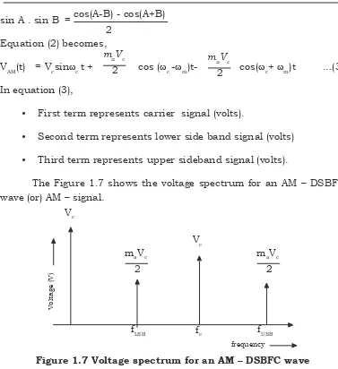
The Figure 1.7 shows the voltage spectrum for an AM – DSBFC
wave (or) AM – signal.
maVc 2
maVc 2 Vc
Vc
fLSB fc fUSB
frequency
Voltage (V)
Figure 1.7 Voltage spectrum for an AM – DSBFC wave
1.8.3 Frequency spectrum of AM
The AM wave is given by,
VAM(t) =Vc(1+ma sin ωmt) sin ωct ...(1)
= Vc(1+ ma sin 2fmt) sin 2fct
=Vcsin 2fct + maVc sin 2pfct sin 2fmt
= maVc
2
maVc
2
carrier USB
LSB
{
{
{
The (-) sign associated with the USB – represents a phase shift of
180 .The figure 1.8 shows the frequency domain representation.
maVc
2
maVc
2
Vc
fc+ fm fc-fm fc
fm f
m
Frequency
Amplitude
BW=2fm
Figure 1.8 Frequency domain representation of AM-wave.
The equation (2) shows the frequency domain representation of AM- signal.
• First term represents the unmodulated carrier signal with the fre-quency of fc
• Second term represents the lower sideband signal with the frequency of ( fc- fm ).
• Third term represents the upper sideband signal with the frequency of ( fc + fm ).
1.8.4 Bandwidth of AM
The bandwidth of the AM-signal is given by the subtraction of the highest frequency component and the lowest frequency component in the frequency spectrum.
BW = Bandwidth = fUSB - fLSB
= ( fc + fm ) - ( fc - fm ) = fc+ fm- fc+fm
Where, BW = Bandwidth is hertz.
fm = Highest modulation frequency in Hertz.
fc = Highest carrier frequency in Hertz.
Thus, the Bandwidth of the AM-signal is the twice that of the maximum frequency of modulating signal.
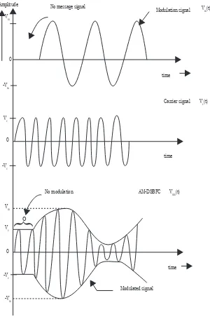
1.8.5 AM- Envelope (or) Graphical representation of AM-wave
AM- DSBFC is sometimes called conventional AM (or) simply AM.
AM is simply called as Double sideband Full carrier (DSBFC) is
probably the most commonly used. The figure 1.9 shows the graphical
representation of AM – signal.
• The shape of the modulated wave (AM) is called AM –envelope which contains all the frequencies and is used to transfer the information through the systems.
• An increase in the modulating signal amplitude causes the amplitude of the carrier to increase.
• Without signal, the AM output waveform is simply the carrier signal.
{
No message signal Modulation signal
time
time
time
Modulated signal AM-DSBFC No modulation
Carrier signal Vm
Vm
-Vm
Vm(t)
VAm(t)
Vc(t) -Vm
Vc
Vc
-Vc -Vc
0
0
0 Amplitude
0
Figure 1.9 AM envelope
1.8.6 Phasor Representation of an AM-wave
The amplitude variation in an AM-system can be explained with
the help of a phasor diagram as shown in figure 1.10
o Carrier
Resultant AM phasor
maVc 2
maVc 2
LSB USB
ωm
-ωm
VAM(t) Vc
Figure 1.10 Phasor representation of AM-wave
• The phasor for the upper sideband rotate anticlockwise at an angular frequency of wm, faster than the carrier frequency ωc (i.e) (ωm>ωc).
• The phasor for the lower sideband rotates clockwise at an angular frequency of wm, slower than the carrier frequency (ωc) (i.e)(ωm<ωc).
• The resulting amplitude of the modulated wave at any instant is the vector sum of the two- sideband phasors.
• Vc is carrier wave phasor, taken as reference phasor and the resulting phasor is VAM (t).
• The phasors for carrier and the upper and lower side frequencies combine, sometimes in phase (adding) and sometimes out of phase (subtracting).
1.8.7 Modulation index and percentage modulation
Modulation index
Modulation index ‘ma’ = Vm Vc
Modulation index is used to describe the amount of amplitude change (modulation) present in an AM – Waveform .
Percentage Modulation
When modulator index is express in percentage, it is called percent modulation.
Percentage modulation gives the percentage changes in the amplitude of the output wave when the carrier is acted on by a modulating signal.
Percentage modulation = Peak amplitude of modulating signal
Peak amplitude of carrier signal x 100
= Vm
Vc x 100 = ma x 100
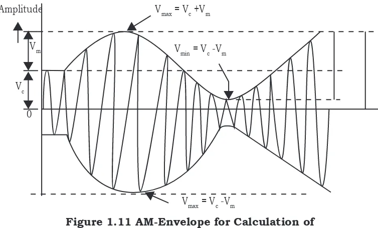
1.8.8 Calculation of modulation index from AM-Waveform
Vmax = Vc +Vm
Vmax = Vc -Vm Vc
Vm V
min = Vc -Vm
Amplitude
0
Figure 1.11 AM-Envelope for Calculation of modulation index
From the figure. 1.11 the maximum and minimum amplitude of
AM-signal is represented by,
Vmax = Vc + Vm ...(1)
Vmin = Vc - Vm ...(2)
From equation (1) - (2) we obtained
Vmax- Vmin = Vc + Vm -Vc + Vm Vmax - Vmin = 2Vm
Vmax = 2Vm + Vmin ...(3)
(or)
Vm = Vmax- Vmin
2 ...(4)
From equation (1) and (2) , the Vc can be calculated as, Equation (1) becomes,
Vc = Vmax - Vm ...(5)
Equation (2) becomes,
Vc = Vmax + Vm ...(6)
From equation (5) vc can be calculated by substitute Vm value,
\ Vc = Vmax - Vmax −Vmin
2
=
2 Vmax -Vmax + Vmin 2
\ Vc =
Vmax + Vmin
2 ...(7)
According to the modulation index definition, the modulation
According to the modulation index definition, the modulation index for AM is given by,
Ma =
Vm
Vc ...(8) Substitute Vm, Vc values in this equation (8)
ma =
Vmax- Vmin/2 Vmax+ Vmin/2
Vmax- Vmin
Vmax+ Vmin
\ma = ...(9)
Percentage of modulation index in terms of Vmax & Vmin can be
ex-pressed as,
Vmax- Vmin Vmax+ Vmin
% ma = x 100
...(10)
The Peak changes in the amplitude of the output wave vm is the sum of the voltages from the upper & lower side frequencies.
Vm 2
VUSB = = VLSB ...(11)
Substituting Vm value in equation (11) we get,
\ VUSB = Vmax- Vmin/2
2 = VLSB
VUSB = VLSB =
Vmax- Vmin
4 ...(12)
Where,
1.8.9 Modulation index for multiple modulating signal frequency
When more than one modulating signals are modulated by a
single carrier, then the modulation index is given by,
ma(t) (or) ma = m
1 2+m
2 2+m
3 2... Where,
ma(or) ma(t) → Total modulation index.
m1,m2... → Modulation index due to individual modulating components.
1.8.10 Degree of modulation
In AM, there are three types of modulations are available. It
depends upon the amplitude of the modulating signal relative to carrier amplitude.
(1) Under modulation.
(2) Critical modulation.
(3) Over modulation.
(1) Under modulation
If Vm<Vc then, the modulation index ma<1
• In this type of modulation , the envelope of amplitude modulated
signal does not reach the zero axis. Hence the message signal is fully preserved in the envelope of the AM wave.
Amplitude
Envelope
time
Figure 1.12 AM wave for Ma <1 (2) Critical modulation
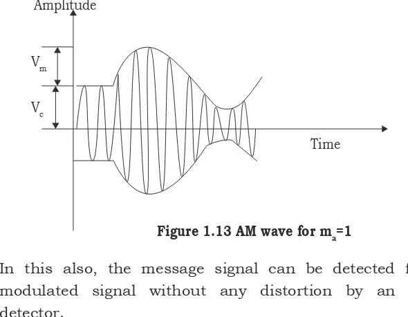
If Vm = Vc , then the modulation index ma=1
In this type of modulation , the envelope of amplitude modulated signal just reaches the zero amplitude axis. The message signal remains preserved.
Vm
Vc
Amplitude
Time
Figure 1.13 AM wave for ma=1
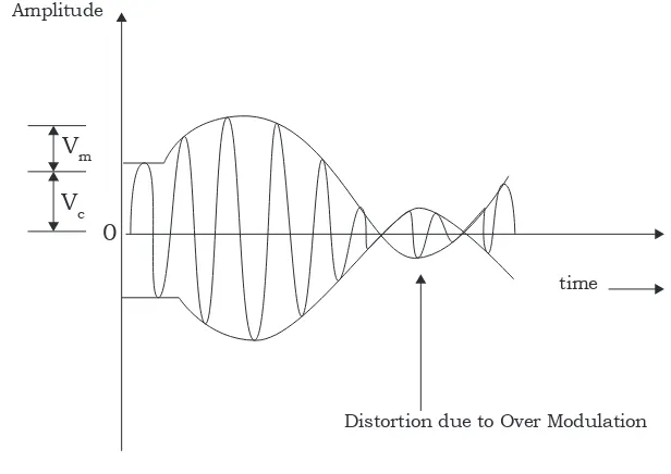
(3) Over modulation
If Vm > Vc ,then the modulation index ma > 1
• Here , both positive and negative extensions of the modulating signals are cancelled (or) clipped out.
Amplitude
time
Distortion due to Over Modulation
Figure 1.14 AM- wave for ma>1 Vm
Vc 0
• The envelope of message signal are not same. Due to this enve-lope detector provides distorted message signal.
• According to the three types of modulation,ma<1, ma=1 ,ma>1. The modulating signals are fully preserved without any distorted from the modulated signal if and only if Vm <Vc then Ma<1
1.8.11 AM-Power distribution
According to the voltage distribution of an AM wave, it consist of three components namely carrier, lower side band and upper side band.
Total transmitted power for AM- signal is given by
Pt = Pc + PLSB + PUSB ...(1) Carrier Power (Pc )
The average power dissipated in a load by an unmodulated carrier is equal to the rms carrier voltage squared divided by the load resistance.
Pc = V
2 carrier
R ...(2)
Pc = (Vc/√2)
2
R
Pc = Vc
2
2R ...(3)
Where,
Pc = Carrier power (watts). Vc = Peak carrier voltage (volts).
R = Load resistance (ohms).
Power in the sidebands
The upper and lower sideband power are expressed mathematically is,
PUSB = PLSB =
(Vsub/ 2)2
R ...(4)
The peak voltage of the upper and lower side band frequencies,
VSUB = maVc
2 ...(5)
Substitute equation (5) in (4)
PUSB = PLSB = [maVc/2] 2) R
(
)
2
PUSB = PLSB = ma2V
c 2
Where,
Total power in AM -wave
Substitute equation (3) and (8) into equation (1), we get
Pt = Pc +PLSB + PUSB
The equation (9) shows the total power required for transmission of AM-signal or DSBFC. The figure 1.15 shows the power spectrum for
Vc2
Figure 1.15 Power spectrum for an AM-wave
For critical modulation ma =1; If ma=1 equation (9) becomes
Total power is 1.5 times of carrier power is for critical modulation.
2 P 1
It = Total transmit current (ampere).
IC = Carrier current (ampere)
R = Antenna resistance (ohms).
We know that, the total transmit power is given by,
Pt =Pc 1
1.8.14 Modulation index in terms of current
Transmission efficiency of an AM-wave is defined as the ratio of
the transmitted power which contains the information (i.e side band power) to the total transmitted power.
=
ma2/2 ma2
2
1 +
x 100
= ma 2/2
(2+ma2)/2
x 100 = ma 2
2+ma2 x 100
ma2
2 +ma2 x 100 % η =
For critical modulation ma =1, then the transmission efficiency becomes,
if ma=1, % η = 12
2+12 x 100 = 1
3 x 100
% η = 33.3 %
The maximum transmission efficiency of the AM-DSBFC is
33.3%.This means , that only one-third of the total power is carried by the sidebands and the rest two-third is a wasted power.
1.8.16 Total transmitted power for AM-DSBSC
Total power required for transmission of AM- DSBSC is depends only on sideband power, because carrier is suppressed.
\Pt = PLSB +PUSB ...(1)
(\Carrier is suppressed)
Sideband powers
The upper and lower sidebands are having equal power which is equal to,
PUSB = PLSB= (Vsub)
2 R
(Vsub/ 2)2 R
= ...(1)a
Vsub = maVc 2
\ Equation (1) becomes
PUSB = PLSB = m Va c/ 2
Substitute equation (2) in (1)
Pt = PLSB +PUSB
For critical modulation, ma=1 Pt = PC 1
2
( )
Pt = 0.5 Pc ...(4)
1.8.17 Transmission efficiency (η) (for AM-DSBSC)
=
The maximum transmission efficiency of AM-DSBSC is 100%. This means the total transmitted power is fully utilized by the AM-
DSBSC. There is no power is wasted.
1.8.18
Comparison of different AM techniquesS.No Parameters DSBFC DSBSC SSB
1. Carrier suppression
Not applicable Fully Fully
2. Sideband suppression
Not applicable Not applicable
6 Complexity Simple Simple Complex
7 Power
requirement to cover are
High Medium Very small
8 Application Radio
1.8.19 Advantages,disadvantages and applications of AM Advantages
• AM is used for long distance communications.
• AM is relatively inexpensive. Disadvantages
• Receiver cost and complexity.
• 66.67% of transmitted power is wasted.
• Large bandwidth is required. Applications
• Sound and audio broadcasting.
• Point to point link communication
• Aircraft communications in the VHF frequency range. Problems
1. What is the bandwidth needed to transmit 4 KHZ voice signal using AM.
Solution
Bandwidth required for AM = 2fm BW =2 fm
BW = 2(4 KHZ)
BW =8 KHZ
2. In an AM –transmitter , the carrier power is 10 KW and the modulation index is 0.5 .calculate the total RF-power delivered.
Solution
Given data
Pc =10 KW
ma = 0.5
The total RF-power delivered Pt = Pc 1 2
2 +
m
a
1 0 5
2 2 +
.
=10 KW
3. The output of AM-transmitter is given by
UAM (t)=500(1+0.4 sin 3140 t)sin 6.28 x 10⁷ t
Calculate
(i) Carrier frequency (ii) Modulating frequency (iii) Modulation index (iv) Carrier power if the load is 600 W (v) Total power.
Solution
The output of AM-DSBFC is given by,
VAM(t)= Vc(1+ ma sinωmt)sinωct ...(1) Compare equation (1)with the given output equation.
We get,
Vc =500 volts
ma =0.4
ωm = 3140 ωc = 6.28 x 10
7 (i) ωm = 2fm = 3140
fm = 3140
2 499.7 fm = 500 HZ
2fc = 6.28 x 107 = w c
(ii) wc = 2pfc = 6.28 x 10⁷
fc = 6.28 x10
7 2
fc = 0.999 x 10⁷ HZ
(iii) Modulation index ma = 0.4
(iv) Carrier power if the load is 600 Ω
Pc = =Vc 2
2R
5002
2 x 600
Pc = 208.3 watts
(v)Total Power (Pt) = P 1 2
2 +
m
a
= 208.3 1 0 4
2 2 +
.
= 224.9
Pt = 225 watts
The total power required for AM is 225 watts.
4. For an AM-DSBFC modulator with a carrier frequency
of 100 KHZ and maximum modulating signal frequency of 5 KHZ.
Determine upper and lower side band frequency and the Bandwidth.
Solution
Given data:
fc =100KHZ fm =5 KHZ
(1)Upper sideband frequency
fUSB =fc +fm
=100 KHZ + 5 KHZ
=105 KHZ
flSb =fc - fm
=100 KHZ - 5 KHZ
=95 KHZ
(3)Bandwidth ‘BW’ =2 fm
=2(5 KHZ)
=10 KHZ
5. In an AM-Modulator, 500 KHZ carrier of amplitude 20 V is modulated
by 10 KHZ modulating signal which causes a change in the output
wave of ± 7.5 V. Determine
(i) Upper and lower sideband frequencies
(ii) Modulation index
(iii) Peak amplitude of upper and lower side frequency.
(iv) Maximum and minimum amplitudes of envelope.
Solution
Given data
fc = 500 KHZ , fm=10 KHZ, Vc= 20 V,Vm=15 V (i) fUSB = fc+fm
= 500 K +10 K
= 510 KHZ
fLSB = fc - fm
= 500 K +10 K
(ii) Modulation index ma = Vm
Vc
= 15
20
= 0.75
(iii) Peak amplitude of upper and lower side frequencies
= maVc
2
= 0.75 x 20
2
= ± 7.5 V
(iv). Maximum and minimum amplitude of envelope.
Vmax = Vc + Vm
= 20 + 15
= 35 V
Vmin = Vc - Vm = 20 - 15
= 5 V
6. If a 10V carrier is amplitude modulated by two different frequencies
with amplitudes 2 V and 3 V respectively. Find modulation index.
Solution
Given data
V
c = 10 V, Vm1 = 2V, Vm2 = 3VModulation index m1 = Vm1
Vc =
2
= 0.2
Modulation index m2 = Vm1
Vc =
3
10 = 0.3
Total modulation index ‘ma’ = m
12 +m2 2 0.04 +0.09
=
ma = 0.66
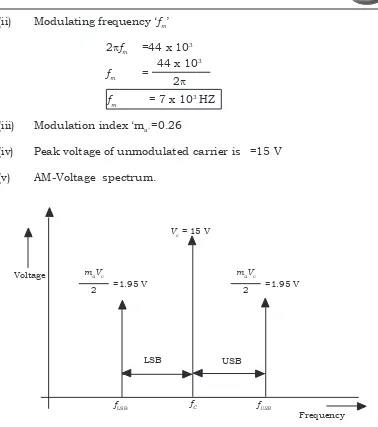
7. An AM-signal has the equation V(t)=[15 + 4 sin 44 x 103 t] (sin 46.5 x 10⁶ t)V. Find
(i)carrier frequency (ii)modulating frequency (iii)modulation index (iv)sketch the signal in the time domain, showing voltage and time scales.(v) Peak voltage of unmodulated carrier.
Solution
V(t) =[15+4 sin 44 x 103 t] sin(46.5 x 10⁶ t) =15[1+ 4
15 sin 44 x 103 t](sin 46.5 x 106 t)
=15[1+ 0.26 sin 44 x 103 t] (sin 46.5 x 10⁶ t) ...(1)
For AM-DSBFC output is given by
V(t) =Vc[1+ma sin ωm t]sin ωct ...(2)
Compare equation (1) and (2) we get,
Vc =15 V
ma = 0.26
ωm = 44 x 10 3 HZ ωc =46.5 x 10
6 HZ
(i) Carrier frequency ‘fc'
2fc = 46.5 x 10
6
f
c =
46.5 x10⁶ 2
f
c =7.4 x 10
(ii) Modulating frequency ‘fm’
2fm =44 x 10
3
f
m =
44 x 103 2
fm = 7 x 10³ HZ
(iii) Modulation index ‘ma’ =0.26
(iv) Peak voltage of unmodulated carrier is =15 V
(v) AM-Voltage spectrum.
Voltage maVc
2 =1.95 V
maVc
2 =1.95 V
Vc = 15 V
LSB USB
Frequency
fLSB fC fUSB
Fig 1.16 AM-Voltage Spectrum
8. For a modulation co-efficient = 0.2 and an unmodulated, carrier
power Pc=1000 W. Determine
(i)Total sideband power (ii)Upper and lower sideband power(iii) modulated carrier power (iv)Total transmitted power.
Solution
Given Data
Un modulated carrier power =1000 W
(i) Upper & lower sideband power,
PUSB =PLSB= ma (ii) The total sideband power is,
PTSB = PUSB + PLSB
(iii)The total power required for transmission of AM-wave,
Pc =PC 1
(iv) Modulated Carrier Power,
1000W = Pc
Pc =1000 watts
9. A 200 W carrier is modulated to a depth of 75%. Calculate the total
power in the modulated wave.
Solution
Given data
Pc =200 W
% ma =75% \ma =0.75 Total power in the modulated wave,
Pt = Pc 1 2
2 +
m
a
= 200 1 0 75
2
2
+
.
Pt = 256.25 watts
10. For an AM-DSBFC wave with an unmodulated carrier voltage of 18V
and a load resistance of 72 W. Determine the following.
(i) Unmodulated carrier power (ii) Modulated carrier power (iii) Total sideband power (iv) Upper & lower sideband power (v) Total transmitted power.
Solution
Given
Vc =18V
(i) Unmodulated carrier power, (ii) Total sideband power,
PTSB =
(iii) upper &lower sideband power,
PUSB =PLSB =
20 KW, for the modulation index is 0.6.
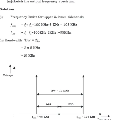
12. For an AM-DSBSC modulator with a carrier frequency fc = 100 KHz and a maximum modulating signal frequency of 5 KHz. Determine.
(i) frequency limits for the upper and lower sidebands.
(ii) Bandwidth
(iii) sketch the output frequency spectrum.
Solution
(i) Frequency limits for upper & lower sidebands,
fUSB = fc+ fm=100 KHz+5 KHz = 105 KHz fLSB = fc- fm=100KHz-5KHz =95KHz
(ii) Bandwidth ‘BW = 2fm = 2 x 5 KHz
=10 KHz
Voltage
BW = 10 KHz
LSB USB
fLSB = 95 KHz fUSB = 105 KHz
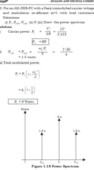
13. For an AM-DSB-FC with a Peak unmodulted carrier voltage Vc=12V,
(iii) Total modulated power,
14. A modulating signal 20 sin (2 x 10³ t) is used to modulate a carrier signal 40 sin (2 x 10⁴ t).Find out,
(i) Modulation index
(ii) Percentage modulation
(iii) Frequencies of the sideband components and their amplitudes.
(iv) Bandwidth of the modulating signal
(v) Also draw the spectrum of the AM-wave.
Solution
Given, modulating signal,
Vm(t) =20 sin(2 x 10³ t) ...(1)
Carrier signal,
Vc(t) = 40 sin (2 x 10⁴ t) ...(2)
(i) Modulating signal, is represented by
Vc(t) = Vm sin (2fmt) ...(3)
Compare , equation (1) & (3),
Vm= 20 V, fm =103 HZ =1 KHZ
(ii) Carrier signal is represented by,
Vc(t) = Vc. sin (2fct) ...(4) Compare equation (2) and (4)
Vc= 40V, fc =104 HZ =10 KHZ
(iii) Modulation index,ma = = Vm
Vc =
20
(iv) Frequency of sideband components,
Upper sideband frequency fUSB= fc+ fm
fUSB = fc+ fm = 10+1 = 11 KHz
Lower sideband frequency,
fUSB = fc-fm = 10-1= 9 KHz
(v) Amplitudes of sidebands
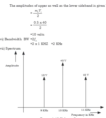
The amplitudes of upper as well as the lower sideband is given by,
= maVc
2
= 0.5 x 40
2
=10 volts
(vi) Bandwidth BW =2fm
=2 x 1 KHZ =2 KHz
(vii) Spectrum
Amplitude
10 V 10 V
40 V
9 KHz 10 KHz 11 KHz
Frequency in KHz
1.9 GENERATION OF SSB
To generate the single side band suppressed carrier (SSBSC), we have to suppress the carrier as well as one of the side bands. The various techniques to suppress one of the side bands are
1. Filter method (or) Frequency discrimination method
2. Phase shift method (or) Hartley Method
3. Third Method (or) Weaver’s Method
1.9.1 Frequency Discrimination method
In Frequency discrimination method, first a DSBSC signal is
generated by using an ordinary product modulator or balanced modulator. Then, this DSBSC signal is passed through
suitable band pass filter to obtain SSBSC signal, where, one of the sidebands is filtered out.
The design of band pass filter is very critical and there are some
limitations on the modulating and carrier frequencies. They are
1. The base band is approximately related to carrier frequency. it is
very difficult to design a band pass filter, If the carrier frequency
is much greater than the bandwidth of the baseband or modu-lating signal.
2. The frequency discrimination method is useful only when the baseband is restricted at its lower edge, so that the upper side bands and lower side bands are non-overlapping.
The filter method is used in speech communication where lowest spectral component is 70Hz and it may not be taken as 300 Hz, without
Product
Figure 1.20 Frequency discrimination method Applications
Since the modulation and demodulation is complex, costlier, this system is not used for commercial broadcasting.
It is mainly used in wireless system for ultra-high frequency and very high frequency communication process.
1.9.2 Phase Discrimination (or) Phase shift method
The block diagram of the phase discriminator is shown in the
figure 1.21
In this method, there are two balanced modulators and two phase shifters used.
One modulator accepts carrier with 90° phase shift from carrier
oscillator and modulating signal directly.
Another modulator accepts modulating signal with phase shift of 900
and the carrier signal directly.
Balanced modulator 1 accepts direct modulating signal
Vm(t) = Vm sinwmt and 90° phase shifted carrier signal
Vc(t) = Vc sin (wct+ 90).
Balanced modulator 2 accepts 90° phase shifted modulating signal
The output of balanced modulator 1 is also, output of balanced
also, output of balanced modulator 2 is
==
(
+)
Therefore, output of the sum will be
0 1 2
1. Each balanced modulator need to be carefully balanced in order to suppress the carrier.
2. Each modulator should have equal sensitivity to baseband signal. 3. It is difficult to design wide band phase shifting network.