3 A Step-Down Voltage Regulator
GENERAL DESCRIPTIONThe LM2596 series of regulators are monolithic integrated circuits that provide all the active functions for a step-down (buck) switching regulator, capable of driving a 3A load with excellent line and load regulation. These devices are available in fixed output voltages of 3.3V, 5V, 12V, and an adjustable output version. Requiring a minimum number of external components, these regulators are simple to use and include internal frequency compensation, and a fixed-frequency oscillator. The LM2596 series operates at a switching frequency of 150 kHz thus allowing smaller sized filter components than what would be needed with lower
frequency switching regulators. Available in a standard 5-lead TO-220 package with several different lead bend options, and a 5-lead TO-263 surface mount package.
A standard series of inductors are available from several different manufacturers optimized for use with the LM2596 series. This feature greatly simplifies the design of switch-mode power supplies.
Other features include a guaranteed ±4% tolerance on output voltage under specified input voltage and output load conditions, and ±15% on the oscillator frequency. External shutdown is included, featuring typically 80 UA standby current. Self protection features include a two stage frequency reducing current limit for the output switch and an over temperature shutdown for complete protection under fault conditions.
FEATURES
• 3.3V, 5V, 12V, and adjustable output versions • Adjustable version output voltage range, 1.2V to 37V • ±4% max over line and load conditions
• Available in TO-220 and TO-263 packages • Guaranteed 3A output load current • Input voltage range up to 40V • Requires only 4 external components
• Excellent line and load regulation specifications • 150 kHz fixed frequency internal oscillator • TTL shutdown capability
• Low power standby mode, IQ typically 80 UA
• High efficiency
• Uses readily available standard inductors • Thermal shutdown and current limit protection
APPLICATIONS
• Simple high-efficiency step-down (buck) regulator • On-card switching regulators
• Positive to negative converter
2
PIN FUNCTIONS
+VIN - This is the positive input supply for the IC switching
regulator. A suitable input bypass capacitor must be present at this pin to minimize voltage transients and to supply the switching currents needed by the regulator.
Ground - Circuit ground.
Output - Internal switch. The voltage at this pin switches between (+VIN - VSAT ) and approximately -0.5V, with a duty
cycle of approximately VOUT /VIN. To minimize coupling to
sensitive circuitry, the PC board copper area connected to this pin should be kept to a minimum.
Feedback #Senses the regulated output voltage to complete the feedback loop.
ON/OFF - Allows the switching regulator circuit to be shut down using logic level signals thus dropping the total input supply current to approximately 80 UA. Pulling this pin below a threshold voltage of approximately 1.3V turns the regulator on, and pulling this pin above 1.3V (up to a maximum of 25V) shuts the regulator down. If this shutdown feature is not needed, the ON /OFF pin can be wired to the ground pin or it can be left open, in either case the regulator will be in the ON condition.
LM2596-3.3
ELECTRICAL CHARACTERISTICS ABSOLUTE MAXIMUM RATINGS (Note 1)
Maximum Supply Voltage 45V
ON /OFF Pin Input Voltage -0.3 ≤ V ≤ +25V Feedback Pin Voltage
Output Voltage to Ground
-0.3 ≤ V ≤+25V (Steady State) -1V Power Dissipation Internally limited Storage Temperature Range ESD
Susceptibility
-650C to +1500C
Human Body Model (Note 2) Lead Temperature S
Package
2 kV
Vapor Phase (60 sec.) +2150C
Infrared (10 sec.) +2450C
T Package (Soldering, 10 sec.) +2600C Maximum
Junction Temperature +1500C
OPERATING CONDITIONS
Temperature Range -40 0C≤T
J≤+1250C
Supply Voltage 4.5V to 40V
Specifications with standard type face are for TJ = 250C, and those with boldface type apply over full Operating Temperature
Range
Symbol Parameter Conditions
LM2596-3.3
Units (Limits) Typ
(Note 3)
Limit (Note 4)
SYSTEM PARAMETERS (Note 5)Test Circuit Figure 1
VOUT Output Voltage 4.7V5≤VIN≤40V, 0.2A≤ILOAD≤3A 3.3
3.168/3.135 3.432/3.465
V V(min) V(max)
η Efficiency VIN=12V, ILOAD=3A 73 %
LM2596-5.0
ELECTRICAL CHARACTERISTICS
Specifications with standard type face are for TJ = 250C, and those with boldface type apply over full Operating Temperature
Range
Symbol Parameter Conditions
LM2596-5.0
Units (Limits) Typ
(Note 3)
Limit (Note 4)
SYSTEM PARAMETERS (Note 5)Test Circuit Figure 1
VOUT Output Voltage 7V≤VIN≤40V, 0.2A≤ILOAD≤3A 5.0
4.800/4.750 5.200/5.250
V V(min) V(max)
η Efficiency VIN=12V, ILOAD=3A 80 %
LM2596-12
ELECTRICAL CHARACTERISTICS
Specifications with standard type face are for TJ = 250C, and those with boldface type apply over full
Operating Temperature Range
Symbol Parameter Conditions
LM2596-12
Units (Limits) Typ
(Note 3)
Limit (Note 4)
VOUT Output Voltage 15V≤VIN≤40V, 0.2A≤ILOAD≤3A 12.0
11.52/11.40 12.48/12.60
V V(min) V(max)
η Efficiency VIN=12V, ILOAD=3A 90 %
LM2596-ADJ
ELECTRICAL CHARACTERISTICS
Specifications with standard type face are for TJ = 250C, and those with boldface type apply over full Operating Temperature
Range
Symbol Parameter Conditions
LM2596-ADJ
Units (Limits) Typ
(Note 3)
Limit (Note 4)
SYSTEM PARAMETERS (Note 5)Test Circuit Figure 1
VOUT Output Voltage 4.5V≤VIN≤40V, 0.2A≤ILOAD≤3A VOUT programmed
for 3V. Circuit of Figure 1.
1.230 1.193/1.180 1.267/1.280 V V(min) V(max)
η Efficiency VIN=12V, VOUT=3V, ILOAD=3A 73 %
ALL OUTPUT VOLTAGE VERSIONS ELECTRICAL CHARACTERISTICS
Specifications with standard type face are for TJ = 250C, and those with boldface type apply over full Operating Temperature
Range. Unless otherwise specified, VIN = 12V for the 3.3V, 5V, and Adjustable version and VIN = 24V for the 12V version. ILOAD =
500 mA
Symbol Parameter Conditions
LM2596-XX
Units (Limits) Typ
(Note 3)
Limit (Note 4)
DEVICE P ARAMETERS
Ib Feedback Bias Current Adjustable Version Only, VFB=1.3V
10
50/100
nA nA (max)
fO Oscillator Frequency (Note 6) 150
127/110 173/173
kHz kHz (min) kHz (max)
VSAT Saturation Voltage IOUT=3A (Notes 7, 8) 1.16
1.4/1.5
V V (max) DC Max Duty Cycle (ON) Min
Duty Cycle (OFF)
(Note 8) (Note 9)
100 0 %
ICL Current Limit Peak Current (Notes 7, 8) 4.5
3.6/3.4 6.9/7.5
A A (min) A (max)
IL Output Leakage Current Output=0V (Notes 7, 9) 50 µA (max)
Output=-1V (Note 10) 2
30
mA mA (max)
IQ Quiescent Current (Note 9) 5
10
mA mA (max) ISTBY Standby Quiescent Current ON/OFF pin=5V (OFF) (Note 10) 80
200/250
µA µA (max) θJC Thermal Resistance TO-220 or TO-263 Package, Junction to Case 2 0C/W
θJA TO-220 Package, Junction to Ambient (Note 11) 50 0C/W
θJA TO-263 Package, Junction to Ambient (Note 12) 50 0C/W
θJA TO-263 Package, Junction to Ambient (Note 13) 30 0C/W
θJA TO-263 Package, Junction to Ambient (Note 14) 20 0C/W
ON/OFF CONTROL Test Circuit Figure 1
VIH VIL
ON/OFF Pin Logic Input Threshold Voltage
Low (Regulator ON) High (Regulator OFF)
1.3
0.6 2.0
V V (max) V
4
IH ON/OFF Pin Input Current VLOGIC=2.5V (Regulator OFF) 5
15
µA µA (max) IL VLOGIC=0.5V (Regulator ON) 0.02
5
µA µA (max) Note 1: Absolute Maximum Ratings indicate limits beyond which damage to the device may occur. Operating Ratings indicate conditions for which the device is intended to be functional, but do not guarantee specific performance limits. For guaranteed specifications and test conditions, see the Electrical Characteristics.
Note 2: The human body model is a 100 pF capacitor discharged through a 1.5k resistor into each pin. Note 3: Typical numbers are at 250C and represent the most likely norm.
Note 4: All limits guaranteed at room temperature (standard type face) and at temperature extremes (bold type face). All room temperature limits are 100% production tested. All limits at temperature extremes are guaranteed via correlation using standard Statistical Quality Control (SQC) methods. All limits are used to calculate Average Outgoing Quality Level (AOQL).
Note 5: External components such as the catch diode, inductor, input and output capacitors, and voltage programming resistors can affect switching regulator system performance. When the LM2596 is used as shown in the Figure 1 test circuit, system performance will be as shown in system parameters section of Electrical Characteristics.
Note 6: The switching frequency is reduced when the second stage current limit is activated. The amount of reduction is determined by the severity of current over-load.
Note 7: No diode, inductor or capacitor connected to output pin.
Note 8: Feedback pin removed from output and connected to 0V to force the output transistor switch ON. Note 9: Feedback pin removed from output and connected to 12V for the 3.3V, 5V, and the ADJ. version, and 15V for the 12V version, to force the output transistor switch OFF.
Note 10: VIN = 40V.
Note 11: Junction to ambient thermal resistance (no external heat sink) for the TO-220 package mounted vertically, with the leads soldered to a printed circuit board with (1 oz.) copper area of approximately 1 in2 Note 12: Junction to ambient thermal
resistance with the TO-263 package tab soldered to a single printed circuit board with 0.5 in2 of (1 oz.) copper area.
Note 13: Junction to ambient thermal resistance with the TO-263 package tab soldered to a single sided printed circuit board with 2.5 in2 of (1 oz.) copper area.
Note 14: Junction to ambient thermal resistance with the TO-263 package tab soldered to a double sided printed circuit board with 3 in2 of (1 oz.) copper area on the LM2596S side of the board, and approximately 16 in2 of copper on the other side of the
p-c board.
TYPICAL PERFORMANCE CHARACTERISTICS (Circuit of Figure 1)
Switch Saturation
6
Operating Shutdown Minimum Operating
Feedback Pin
Bias Current
TYPICAL PERFORMANCE CHARACTERISTICS
Discontinuous Mode Switching Waveforms
VIN=20V, VOUT=5V, ILOAD=500mA
B: Inductor Current 1A/div
C: Output Ripple Voltage, 50mV/div
Horizontal Time Base: 2µs/div
Load Transient Response for Continuous Mode VIN=20V, VOUT=5V, ILOAD=500mA to 2A
A: Output Voltage, 100mV/div.(AC) B: 500mA to 2A Load Pulse
Horizontal Time Base: 100
µ
s/div
A: Output Pin Voltage, 10V/div B: Inductor Current 1A/div
C: Output Ripple Voltage, 100mV/div
Horizontal Time Base: 2µs/div
Load Transient Response for Discontinuous Mode VIN=20V, VOUT=5V, ILOAD=500mA to 2A
A: Output Voltage, 100mV/div. (AC) B: 500mA to 2A Load Pulse
Horizontal Time Base: 200
µ
s/div
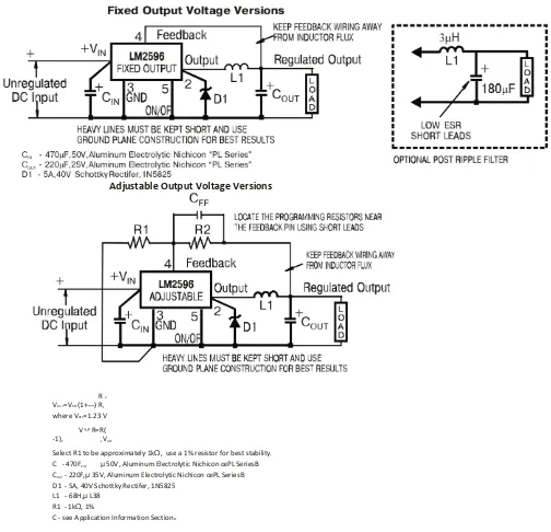
TEST CIRCUIT AND LAYOUT GUIDELINES
8
Adjustable Output Voltage Versions
R 2
VOUT=VREF(1+ ) R1 where VREF=1.23 V
V OUT R=R( -1)2 1 VREF
Select R1 to be approximately 1kΩ, use a 1% resistor for best stability. C - 470F,IN µ50V, Aluminum Electrolytic Nichicon œPL SeriesB COUT - 220F,µ35V, Aluminum Electrolytic Nichicon œPL SeriesB D1 - 5A, 40V Schottky Rectifer, 1N5825
L1 - 68H,µ L38 R1 - 1kΩ, 1%
C - see Application Information SectionFF
Figure 1. Standard Test Circuits and Layout Guides
As in any switching regulator, layout is very important. Rapidly switching currents associated with wiring inductance can generate voltage transients which can cause problems. For minimal inductance and ground loops, the wires indicated by heavy lines should be wide printed circuit traces and should be kept as short as possible. For best results, external components should be located as close to the switcher lC as possible using ground plane construction or single point grounding.
If open core inductors are used, special care must be taken as to the location and positioning of this type of inductor. Allowing the inductor flux to intersect sensitive feedback, lC groundpath and COUT wiring can cause problems.
When using the adjustable version, special care must be taken as to the location of the feedback resistors and the associated wiring. Physically locate both resistors near the IC, and route the wiring away from the inductor, especially an open core type of inductor.
LM2596 SERIES BUCK REGULATOR DESIGN PROCEDURE (FIXED OUTPUT)
PROCEDURE (Fixed Output Voltage Version) EXAMPLE (Fixed Output Voltage Version)
Given: Given:
VOUT = Regulated Output Voltage (3.3V, 5V or 12V) VOUT =5V
ILOAD (max) = Maximum Load Current ILOAD (max) = 3A
1. Inductor Selection (L1) 1. Inductor Selection (L1)
A. Select the correct inductor value selection guide from Figures Figure 4, Figure 5,or Figure 6. (Output voltages of 3.3V, 5V, or 12V respectively.) For all other voltages, see the design procedure for the adjustable version.
A. Use the inductor selection guide for the 5V version shown in Figure 5.
B. From the inductor value selection guide, identify the
inductance region intersected by the Maximum Input Voltage line and the Maximum Load Current line. Each region is identified by an inductance value and an inductor code (LXX).
B. From the inductor value selection guide shown in Figure 5, the inductance region intersected by the 12V horizontal line and the 3A vertical line is 33 UH, and the inductor code is L40.
C. Select an appropriate inductor from the four manufacturer’s part numbers listed in Figure 8.
C. The inductance value required is 33 UH. From the table in Figure 8, go to the L40 line and choose an inductor part number from any of the four manufacturers shown. (In most in-stance, both through hole and surface mount inductors are available.)
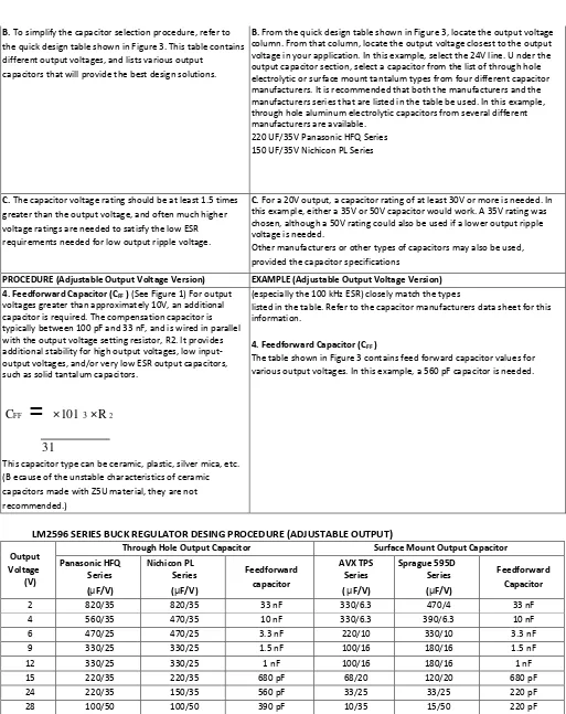
2. Output Capacitor Selection (COUT)
2. Output Capacitor Selection (COUT)
A. In the majority of applications, low ESR (Equivalent
Series Resistance) electrolytic capacitors between 82 UF and 820 UF and low ESR solid tantalum capacitors between 10 UF and 470 UF provide the best results. This capacitor should be located close to the IC using short capacitor leads and short copper traces. Do not use capacitors larger than 820 UF.
A. See section on output capacitors in application information section.
B. To simplify the capacitor selection procedure, refer to the quick design component selection table shown in Figure 2. This table contains different input voltages, output voltages, and load currents, and lists various inductors and output capacitors that will provide the best design solutions.
B. From the quick design component selection table shown in Figure 2, locate the 5V output voltage section. In the load current column, choose the load current line that is closest to the current needed in your application, for this example, use the 3A line. In the maximum input voltage column, select the line that covers the input voltage needed in your application, in this example, use the 15V line. Continuing on this line are recommended inductors and capacitors that will provide the best overall performance. The capacitor list contains both through hole electrolytic and surface mount tantalum capacitors from four different capacitor manufacturers. It is recommended that both the
manufacturers and the manufacturer’s series that are listed in the table be used. In this example aluminum electrolytic capacitors from several different manufacturers are available with the range of ESR numbers needed.
330 UF 35V Panasonic HFQ Series 330 UF 35V Nichicon PL Series C. The capacitor voltage rating for electrolytic capacitors should
be at least 1.5 times greater than the output voltage, and often much higher voltage ratings are needed to satisfy the low ESR requirements for low output ripple voltage.
C. For a 5V output, a capacitor voltage rating at least 7.5V or more is needed. B ut even a low ESR, switching grade, 220UF 10V aluminum electrolytic capacitor would exhibit approximately
225 mW of ESR (see the curve in Figure 14 for the ESR vs voltage rating). This amount of ESR would result in relatively high output ripple voltage. To reduce the ripple to 1% of the output voltage, or less, a capacitor with a higher value or with a higher voltage rating (lower ESR) should be selected. A 16V or 25V capacitor will reduce the ripple volt-age by approximately half.
3. Catch Diode Selection (D1) 3. Catch Diode Selection (D1) A. The catch diode current rating must be at least 1.3 times
greater than the maximum load current. Also, if the power supply design must withstand a continuous output short, the diode should have a current rating equal to the maximum current limit of the LM2596. The most stressful condition for this diode is an overload or shorted output condition.
A. Refer to the table shown in Figure 11. In this example, a 5A, 20V, 1N5823 Schottky diode will provide the best performance, and will not be overstressed even for a shorted output.
B. The reverse voltage rating of the diode should be at least 1.25 times the maximum input voltage.
10
PROCEDURE (Fixed Output Voltage Version) EXAMPLE (Fixed Output Voltage Version) and must be located close to the LM2596 using short leads and
short printed circuit traces. B ecause of their fast switching speed and low forward voltage drop, Schottky diodes provide the best performance and efficiency, and should be the first choice, especially in low output voltage applications.
Ultra-fast recovery, or High-Efficiency rectifiers also provide good results. Ultra-fast recovery diodes typically have reverse recovery times of 50 ns or less. Rectifiers such as the 1N5400 series are much too slow and should not be used.
4. Input Capacitor (CIN) 4. Input Capacitor (CIN)
A low ESR aluminum or tantalum bypass capacitor is needed between the input pin and ground pin to prevent large volt-age transients from appearing at the input. This capacitor should be located close to the IC using short leads. In addition, the RMS current rating of the input capacitor should be selected to be at least 1/2 the DC load current. The capacitor manufacturers data sheet must be checked to assure that this current rating is not exceeded. The curve shown in Figure 9 shows typical RMS current ratings for several different aluminum electrolytic capacitor values.
For an aluminum electrolytic, the capacitor voltage rating should be approximately 1.5 times the maximum input voltage. The tantalum capacitor voltage rating should be 2 times the maximum input voltage and it is recommended that they be surge current tested by the manufacturer. Use caution when using ceramic capacitors for input bypassing, because it may cause severe ringing at the VIN pin.
The important parameters for the Input capacitor are the input voltage rating and the RMS current rating. With a nominal input voltage of 12V, an aluminum electrolytic capacitor with a voltage rating greater than 18V (1.5 x VIN ) would be needed. The next higher capacitor voltage rating is
25V.
The RMS current rating requirement for the input capacitor in a buck regulator is approximately 1 /2 the DC load current. In this
example, with a 3A load, a capacitor with a RMS current rating of at least 1.5A is needed. The curves shown in Figure 9 can be used to select an appropriate input capacitor.
From the curves, locate the 35V line and note which capacitor values have RMS current ratings greater than 1.5A. A 680UF/35V capacitor could be used.
For a through hole design, a 680UF/35V electrolytic capacitor (Panasonic HFQ series or Nichicon PL series or equivalent) would be adequate. other types or other manufacturers capacitors can be used provided the RMS ripple current ratings are adequate. For surface mount designs, solid tantalum capacitors can be used, but caution must be exercised with regard to the capacitor surge current rating. The TPS series available from AVX, and the 593D series from Sprague are both surge current tested.
LM2596 SERIES BUCK REGULATOR DESIGN PROCEDURE (FIXED OUTPUT) (Continued)
Conditions Inductor Output Capacitor
Through Hole Electrolytic Surface Mount Tantalum Output Voltage (V) Load Current (A) Max Input Voltage (V) Inductance ( µH) Inductor (#) Panasonic HFQ Series ( µF/V)
Nichicon PL Series (µF/V)
AVX TPS Series
(µF/V)
Sprague 595D Series (µF/V)
3.3 3 5 22 L41 470/25 560/16 330/6.3 390/6.3
7 22 L41 560/35 560/35 330/6.3 390/6.3
10 22 L41 680/35 680/35 330/6.3 390/6.3
40 33 L40 560/35 470/35 330/6.3 390/6.3
2 6 22 L33 470/25 470/35 330/6.3 390/6.3
10 33 L32 330/35 330/35 330/6.3 390/6.3
40 47 L39 330/35 270/50 220/10 330/10
5 3 8 22 L41 470/25 560/16 220/10 330/10
10 22 L41 560/25 560/25 220/10 330/10
15 33 L40 330/35 330/35 220/10 330/10
40 47 L39 330/35 270/35 220/10 330/10
2 9 22 L33 470/25 560/16 220/10 330/10
20 68 L38 180/35 180/35 100/10 270/10
40 68 L38 180/35 180/35 100/10 270/10
12 3 15 22 L41 470/25 470/25 100/16 180/16
18 33 L40 330/25 330/25 100/16 180/16
40 68 L44 180/35 180/35 100/16 120/20
2 15 33 L32 330/25 330/25 100/16 180/16
20 68 L38 180/25 180/25 100/16 120/20
40 150 L42 82/25 82/25 68/20 68/25
Figure 2. LM2596 Fixed Voltage Quick Design Component Selection Table
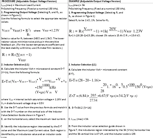
LM2596 SERIES BUCK REGULATOR DESIGN PROCEDURE (ADJUSTABLE OUTPUT)
PROCEDURE (Adjustable Output Voltage Version) EXAMPLE (Adjustable Output Voltage Version)
Given: Given:
VOUT = Regulated Output Voltage VOUT = 20V
12
PROCEDURE (Adjustable Output Voltage Version) EXAMPLE (Adjustable Output Voltage Version) ILOAD(max) = Maximum Load Current ILOAD(max) = 3A
F=Switching Frequency (Fixed at a nominal 150 kHz). F=Switching Frequency (Fixed at a nominal 150 kHz). 1. Programming Output Voltage (Selecting R1 and R2, as
shown in Figure 1)
Use the following formula to select the appropriate resistor values.
VOUT
=
VREF(1+ R
2) where
VREF
=
1.23V
R
1Select a value for R1 between 240Ω and 1.5kΩ. The lower
resistor values minimize noise pickup in the sensitive feedback pin. (For the lowest temperature coefficient and the best stability with time, use 1% metal film resistors.)
R
2=
R
1(V
OUT−
1)
V
REF1. Programming Output Voltage (Selecting R1 and
R2, as shown in Figure 1)
Select R1 to be 1 kΩ, 1%. Solve for R2.
R
2=
R
1(
V
OUT−
1)
=
1k(
20V
−
1)
V
REF1.23V
R2=1 k (16.26-1)=15.26k, closest 1% value is 15.4k Ω R 2= 15.4 kΩ.2. Inductor Selection (L1) 2. Inductor Selection (L1)
A. Calculate the inductor Volt • microsecond constant E•T (V•Us), from the following formula:
E
•
T=(V
IN−
V
OUT−
V
SAT)
•
V
−
OUTV
SAT+V
+
D D•
150
1000
kHz
(V
•µ
s)
V
INV
where VSAT = internal switch saturation voltage = 1.16V and
VD = diode forward voltage drop = 0.5V
A. Calculate the inductor Volt • microsecond constant (E•T),
E
•
T=(28
−
20
−
1.16)
•
−
20
1.
+
16
0.
+
5
0.5
•
100
150
0
(V
•µ
s)
28
E
•
T =(6.84)
•
•
6.67(V
•µ
s)=34.2(V
•µ
s)
B. Use the E•T value from the previous formula and match it with the E•T number on the vertical axis of the Inductor Value Selection Guide shown in Figure 7.
B. E•T=34.2 (V•Us)
C. on the horizontal axis, select the maximum load current. C. ILOAD (max) = 3A
D. Identify the inductance region intersected by the E•T value and the Maximum Load Current value. Each region is identified by an inductance value and an inductor code (LXX).
D. From the inductor value selection guide shown in
Figure 7, the inductance region intersected by the 34 (V•Us) horizontal line and the 3A vertical line is 47 UH, and the inductor code is L39.
E. Select an appropriate inductor from the four manufacturer’s part numbers listed in Figure 8.
E. From the table in Figure 8, locate line L39, and select an inductor part number from the list of manufacturers part numbers.
3. Output Capacitor Selection (COUT)
A. In the majority of applications, low ESR electrolytic or solid tantalum capacitors between 82 UF and 820 UF provide the best results. This capacitor should be located close to the IC using short capacitor leads and short copper traces. Do not use capacitors larger than 820 UF.
B. To simplify the capacitor selection procedure, refer to the quick design table shown in Figure 3. This table contains different output voltages, and lists various output
capacitors that will provide the best design solutions.
B. From the quick design table shown in Figure 3, locate the output voltage column. From that column, locate the output voltage closest to the output voltage in your application. In this example, select the 24V line. U nder the output capacitor section, select a capacitor from the list of through hole electrolytic or surface mount tantalum types from four different capacitor manufacturers. It is recommended that both the manufacturers and the manufacturers series that are listed in the table be used. In this example, through hole aluminum electrolytic capacitors from several different manufacturers are available.
220 UF/35V Panasonic HFQ Series 150 UF/35V Nichicon PL Series
C. The capacitor voltage rating should be at least 1.5 times greater than the output voltage, and often much higher voltage ratings are needed to satisfy the low ESR requirements needed for low output ripple voltage.
C. For a 20V output, a capacitor rating of at least 30V or more is needed. In this example, either a 35V or 50V capacitor would work. A 35V rating was chosen, although a 50V rating could also be used if a lower output ripple voltage is needed.
Other manufacturers or other types of capacitors may also be used, provided the capacitor specifications
PROCEDURE (Adjustable Output Voltage Version) EXAMPLE (Adjustable Output Voltage Version) 4. Feedforward Capacitor (CFF ) (See Figure 1)For output
voltages greater than approximately 10V, an additional capacitor is required. The compensation capacitor is typically between 100 pF and 33 nF, and is wired in parallel with the output voltage setting resistor, R2. It provides additional stability for high output voltages, low input-output voltages, and/or very low ESR input-output capacitors, such as solid tantalum capacitors.
C
FF=
×
101
3×
R
231
This capacitor type can be ceramic, plastic, silver mica, etc. (B ecause of the unstable characteristics of ceramic capacitors made with Z5U material, they are not recommended.)
(especially the 100 kHz ESR) closely match the types
listed in the table. Refer to the capacitor manufacturers data sheet for this information.
4. Feedforward Capacitor (CFF )
The table shown in Figure 3 contains feed forward capacitor values for various output voltages. In this example, a 560 pF capacitor is needed.
LM2596 SERIES BUCK REGULATOR DESING PROCEDURE (ADJUSTABLE OUTPUT)
Output Voltage (V)
Through Hole Output Capacitor Surface Mount Output Capacitor Panasonic HFQ
Series (µF/V)
Nichicon PL Series (µF/V)
Feedforward capacitor
AVX TPS Series ( µF/V)
Sprague 595D Series (µF/V)
Feedforward Capacitor
2 820/35 820/35 33 nF 330/6.3 470/4 33 nF
4 560/35 470/35 10 nF 330/6.3 390/6.3 10 nF
6 470/25 470/25 3.3 nF 220/10 330/10 3.3 nF
9 330/25 330/25 1.5 nF 100/16 180/16 1.5 nF
12 330/25 330/25 1 nF 100/16 180/16 1 nF
15 220/35 220/35 680 pF 68/20 120/20 680 pF
24 220/35 150/35 560 pF 33/25 33/25 220 pF
28 100/50 100/50 390 pF 10/35 15/50 220 pF
Figure 3. Output Capacitor and Feedforward Capacitor Selection Table
LM2596 SERIES BUCK REGULATOR DESIGN PROCEDURE
14
MAXIMUM LOAD CURRENT (A) MAXIMUM LOAD CURRENT (A)
Figure 4. LM2596-3.3 Figure 6. LM2596-12
MAXIMUM LOAD CURRENT (A)
Figure 5. LM2596-5.0
MAXIMUM LOAD CURRENT (A)
LM2596 SERIES BUCK REGULATOR DESIGN PROCEDURE (Continued)
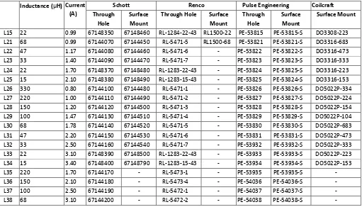
Inductance (µH) Current (A)
Schott Renco Pulse Engineering Coilcraft
Through Hole
Surface Mount
Through Hole Surface Mount
Through Hole
Surface Mount
Surface Mount
L15 22 0.99 67148350 67148460 RL-1284-22-43 RL1500-22 PE-53815 PE-53815-S DO3308-223 L21 68 0.99 67144070 67144450 RL-5471-5 RL1500-68 PE-53821 PE-53821-S DO3316-683 L22 47 1.17 67144080 67144460 RL-5471-6 - PE-53822 PE-53822-S DO3316-473 L23 33 1.40 67144090 67144470 RL-5471-7 - PE-53823 PE-53823-S DO3316-333 L24 22 1.70 67148370 67148480 RL-1283-22-43 - PE-53824 PE-53825-S DO3316-223 L25 15 2.10 67148380 67148490 RL-1283-15-43 - PE-53825 PE-53824-S DO3316-153 L26 330 0.80 67144100 67144480 RL-5471-1 - PE-53826 PE-53826-S DO5022P-334 L27 220 1.00 67144110 67144490 RL-5471-2 - PE-53827 PE-53827-S DO5022P-224 L28 150 1.20 67144120 67144500 RL-5471-3 - PE-53828 PE-53828-S DO5022P-154 L29 100 1.47 67144130 67144510 RL-5471-4 - PE-53829 PE-53829-S DO5022P-104 L30 68 1.78 67144140 67144520 RL-5471-5 - PE-53830 PE-53830-S DO5022P-683 L31 47 2.20 67144150 67144530 RL-5471-6 - PE-53831 PE-53831-S DO5022P-473 L32 33 2.50 67144160 67144540 RL-5471-7 - PE-53932 PE-53932-S DO5022P-333 L33 22 3.10 67148390 67148500 RL-1283-22-43 - PE-53933 PE-53933-S DO5022P-223 L34 15 3.40 67148400 67148790 RL-1283-15-43 - PE-53934 PE-53934-S DO5022P-153
L35 220 1.70 67144170 - RL-5473-1 - PE-53935 PE-53935-S -
L36 150 2.10 67144180 - RL-5473-4 - PE-54036 PE-54036-S -
L37 100 2.50 67144190 - RL-5472-1 - PE-54037 PE-54037-S -
L39 47 3.50 67144210 - RL-5472-3 - PE-54039 PE-54039-S -
L40 33 3.50 67144220 67148290 RL-5472-4 - PE-54040 PE-54040-S -
L41 22 3.50 67144230 67148300 RL-5472-5 - PE-54041 PE-54041-S -
L42 150 2.70 67148410 - RL-5473-4 - PE-54042 PE-54042-S -
L43 100 3.40 67144240 - RL-5473-2 - PE-54043 -
L44 68 3.40 67144250 - RL-5473-3 - PE-54044 -
Figure 8. Inductor Manufacturers Part Numbers
PAD DIAGRAM
Chip Size 4.2 x 2.7 mm2
PAD LOCATIONS COORDINATES
Pad N
Pad Name Pad Size µm Coordinates µm
X Y
1 VIN 200 x 400 210 2023
1 VIN 505 x 205 1412 1911
2 Out 205 x 400 925 720
3 GND 200 x 200 2461 2454
3 GND 200 x 200 3578 2454
3 GND 200 x 200 3921 1174
4 FB 200 x 200 3980 220
5 ON/OFF 200 x 200 3848 2454
TO−220
-5L
Vin
Pin 1.
2. Output 3. Ground
4. Feedback 5. ON
SEATING
0.356 (0.014) M
T Q
M
TO−263
-5L(D2PAK)
1 5
Pin 1. Vin
2. Output 3. Ground 4. Feedback
5. ON
DIM
INCHES MILLIMETERS MIN MAX MIN MAX A 0.572 0.613 14.529 15.570 B 0.390 0.415 9.906 10.541 B1 0.375 0.415 9.525 10.541 C 0.170 0.180 4.318 4.572 D 0.025 0.038 0.635 0.965 E 0.048 0.055 1.219 1.397 G 0.067 BSC 1.70 2 BSC H 0.087 0.112 2.210 2.845
J 0.015 0.025 0.381 0.635 K 0.977 1.045 24.810 26.543 L 0.320 0.365 8.128 9.271 Q 0.140 0.153 3.556 3.886 U 0.105 0.117 2.667 2.972
DIM
INCHES MILLIMETERS MIN MAX MIN MAX A 0.386 0.403 9.804 10.236
B 0.356 0.368 9.042 9.347
C 0.170 0.180 4.318 4.572
D 0.026 0.036 0.660 0.914
E 0.045 0.055 1.143 1.397
G 0.067 BSC 1.70 2 BSC
L 0.000 0.010 0.000 0.254
M 0.088 0.102 2.235 2.591
N 0.018 0.026 0.457 0.660
P 0.058 0.078 1.473 1.981
R 5 REF 5 REF
S 0.116 REF 2.946 REF
U 0.200 MIN 5.080 MIN
V 0.250 MIN 6.350 MIN
0.010 (0.254)
M