ELECTRONIC
PRINCIPLES
ALBERT MALVINO | DAVID BATES
ELECTRONIC PRINCIPLES, EIGHTH EDITION
Published by Hill Education, 2 Penn Plaza, New York, NY 10121. Copyright 2016 by McGraw-Hill Education. All rights reserved. Printed in the United States of America. Previous edition © 2007. No part of this publication may be reproduced or distributed in any form or by any means, or stored in a data-base or retrieval system, without the prior written consent of McGraw-Hill Education, including, but not limited to, in any network or other electronic storage or transmission, or broadcast for distance learning. Some ancillaries, including electronic and print components, may not be available to customers outside the United States.
This book is printed on acid-free paper. 1 2 3 4 5 6 7 8 9 0 DOW/DOW 1 0 9 8 7 6 5 ISBN 978-0-07-337388-1
MHID 0-07-337388-5
Senior Vice President, Products & Markets: Kurt L. Strand Vice President, General Manager, Products & Markets: Marty Lange Director of Digital Content: Thomas Scaife, Ph.D
Vice President, Content Design & Delivery: Kimberly Meriwether David Managing Director: Thomas Timp
Global Publisher: Raghu Srinivasan Director, Product Development: Rose Koos Product Developer: Vincent Bradshaw Marketing Manager: Nick McFadden
Director, Content Design & Delivery: Linda Avenarius Executive Program Manager: Faye M. Herrig
Content Project Managers: Jessica Portz, Tammy Juran, & Sandra Schnee Buyer: Susan K. Culbertson
Design: Studio Montage, St. Louis, MO Content Licensing Specialist: DeAnna Dausener Cover Image: Royalty-Free/CORBIS
Compositor: MPS Limited Typeface: 10/12 Times New Roman Printer: R.R. Donnelley
All credits appearing on page or at the end of the book are considered to be an extension of the copyright page. Library of Congress Cataloging-in-Publication Data
Malvino, Albert Paul.
Electronic principles/Albert Malvino, David J. Bates.—Eighth edition. pages cm
ISBN 978-0-07-337388-1 (alk. paper) 1. Electronics. I. Bates, David J. II. Title. TK7816.M25 2015
621.381—dc23
2014036290
The Internet addresses listed in the text were accurate at the time of publication. The inclusion of a website does not indicate an endorsement by the authors or McGraw-Hill Education, and McGraw-Hill Education does not guarantee the accuracy of the information presented at these sites.
Albert P. Malvino was an electronics technician while serving in the U.S. Navy from 1950 to 1954. He graduated from the University of Santa Clara Summa Cum Laude in 1959 with a B.S. degree in Electrical Engineering. For the next fi ve years, he worked as an electronics engineer at Microwave Laboratories and at Hewlett-Packard while earning his MSEE from San Jose State University in 1964. He taught at Foothill College for the next four years and was awarded a National Science Foundation Fellowship in 1968. After receiving a Ph.D. in Electrical Engineering from Stanford University in 1970, Dr. Malvino embarked on a full-time writing career. He has written 10 textbooks that have been translated into 20 foreign languages with over 108 editions. Dr. Malvino was a consultant and designed control circuits for SPD-Smart™ windows. In addition, he wrote educational software for electronics technicians and engineers. He also served on the Board of Directors at Research Frontiers Incorporated. His website address is www.malvino.com
David J. Bates is an adjunct instructor in the Electronic Technologies Department of Western Wisconsin Technical College located in La Crosse, Wisconsin. Along with working as an electronic servicing technician and as an electrical engineering technician, he has over 30 years of teaching experience.
Credentials include an A.S. degree in Industrial Electronics Technology, a B.S. degree in Industrial Education, and an M.S. degree in Vocational/Technical Education. Certifi cations include an A1 certifi cation as a computer hardware technician, and Journeyman Level certifi cations as a Certifi ed Electronics Technician (CET) by the Electronics Technicians Association International (ETA-I) and by the International Society of Certifi ed Electronics Technicians (ISCET). David J. Bates is presently a certifi cation administrator (CA) for ETA-I and ISCET and has served as a member of the ISCET Board of Directors, along with serving as a Subject Matter Expert (SME) on basic electronics for the National Coalition for Electronics Education (NCEE).
David J. Bates is also a co-author of “Basic Electricity” a text-lab manual by Zbar, Rockmaker, and Bates.
Dedication
iv
Contents
Preface ix
Chapter 1
Introduction 02
1-1 The Three Kinds of Formulas
1-2 Approximations
1-3 Voltage Sources
1-4 Current Sources
1-5 Thevenin’s Theorem
1-6 Norton’s Theorem
1-7 Troubleshooting
Chapter 2
Semiconductors 28
2-1 Conductors
2-2 Semiconductors
2-3 Silicon Crystals
2-4 Intrinsic Semiconductors
2-5 Two Types of Flow
2-6 Doping a Semiconductor
2-7 Two Types of Extrinsic Semiconductors
2-8 The Unbiased Diode
2-9 Forward Bias
2-10 Reverse Bias
2-11 Breakdown
2-12 Energy Levels
2-13 Barrier Potential and Temperature
2-14 Reverse-Biased Diode
Chapter 3
Diode Theory 56
3-1 Basic Ideas
3-2 The Ideal Diode
3-3 The Second Approximation
3-4 The Third Approximation
3-5 Troubleshooting
3-6 Reading a Data Sheet
3-7 How to Calculate Bulk Resistance
3-8 DC Resistance of a Diode
3-9 Load Lines
3-10 Surface-Mount Diodes
3-11 Introduction to Electronic Systems
Chapter 4
Diode Circuits 86
4-1 The Half-Wave Rectifi er
4-2 The Transformer
4-3 The Full-Wave Rectifi er
4-4 The Bridge Rectifi er
4-5 The Choke-Input Filter
4-6 The Capacitor-Input Filter
4-7 Peak Inverse Voltage and Surge Current
4-8 Other Power-Supply Topics
4-9 Troubleshooting
4-10 Clippers and Limiters
4-11 Clampers
Chapter 5
Special-Purpose Diodes 140
5-1 The Zener Diode
5-2 The Loaded Zener Regulator
5-3 Second Approximation of a Zener Diode
5-4 Zener Drop-Out Point
5-5 Reading a Data Sheet
5-6 Troubleshooting
5-7 Load Lines
5-8 Light-Emitting Diodes (LEDs)
5-9 Other Optoelectronic Devices
5-10 The Schottky Diode
5-11 The Varactor
5-12 Other Diodes
Chapter 6
BJT Fundamentals 188
6-1 The Unbiased Transistor
6-2 The Biased Transistor
6-3 Transistor Currents
6-4 The CE Connection
6-5 The Base Curve
6-6 Collector Curves
6-7 Transistor Approximations
6-8 Reading Data Sheets
6-9 Surface-Mount Transistors
6-10 Variations in Current Gain
6-11 The Load Line
6-12 The Operating Point
6-13 Recognizing Saturation
6-14 The Transistor Switch
6-15 Troubleshooting
Chapter 7
BJT Biasing 240
7-1 Emitter Bias
7-2 LED Drivers
7-3 Troubleshooting Emitter Bias Circuits
7-4 More Optoelectronic Devices
7-5 Voltage-Divider Bias
7-6 Accurate VDB Analysis
7-7 VDB Load Line and Q Point
7-8 Two-Supply Emitter Bias
7-9 Other Types of Bias
7-10 Troubleshooting VDB Circuits
7-11 PNP Transistors
Chapter 8
Basic BJT Amplifi ers 280
8-1 Base-Biased Amplifi er
8-2 Emitter-Biased Amplifi er
8-3 Small-Signal Operation
8-4 AC Beta
8-5 AC Resistance of the Emitter Diode
8-6 Two Transistor Models
8-7 Analyzing an Amplifi er
8-8 AC Quantities on the Data Sheet
8-9 Voltage Gain
8-10 The Loading Eff ect of Input Impedance
8-11 Swamped Amplifi er
8-12 Troubleshooting
Chapter 9
Multistage, CC, and CB
Amplifi ers 326
9-1 Multistage Amplifi ers
9-2 Two-Stage Feedback
9-3 CC Amplifi er
9-4 Output Impedance
9-5 Cascading CE and CC
9-6 Darlington Connections
9-7 Voltage Regulation
9-8 The Common-Base Amplifi er
vi Contents
Chapter 10
Power Amplifi ers 366
10-1 Amplifi er Terms
10-2 Two Load Lines
10-3 Class-A Operation
10-4 Class-B Operation
10-5 Class-B Push-Pull Emitter Follower
10-6 Biasing Class-B/AB Amplifi ers
10-7 Class-B/AB Driver
10-8 Class-C Operation
10-9 Class-C Formulas
10-10 Transistor Power Rating
Chapter 11
JFETs 414
11-1 Basic Ideas
11-2 Drain Curves
11-3 The Transconductance Curve
11-4 Biasing in the Ohmic Region
11-5 Biasing in the Active Region
11-6 Transconductance
11-7 JFET Amplifi ers
11-8 The JFET Analog Switch
11-9 Other JFET Applications
11-10 Reading Data Sheets
11-11 JFET Testing
Chapter 12
MOSFETs 470
12-1 The Depletion-Mode MOSFET
12-2 D-MOSFET Curves
12-3 Depletion-Mode MOSFET Amplifi ers
12-4 The Enhancement-Mode MOSFET
12-5 The Ohmic Region
12-6 Digital Switching
12-7 CMOS
12-8 Power FETs
12-9 High-Side MOSFET Load Switches
12-10 MOSFET H-Bridge
12-11 E-MOSFET Amplifi ers
12-12 MOSFET Testing
Chapter 13
Thyristors 524
13-1 The Four-Layer Diode
13-2 The Silicon Controlled Rectifi er
13-3 The SCR Crowbar
13-4 SCR Phase Control
13-5 Bidirectional Thyristors
13-6 IGBTs
13-7 Other Thyristors
13-8 Troubleshooting
Chapter 14
Frequency Eff ects 568
14-1 Frequency Response of an Amplifi er
14-2 Decibel Power Gain
14-3 Decibel Voltage Gain
14-4 Impedance Matching
14-5 Decibels above a Reference
14-6 Bode Plots
14-7 More Bode Plots
14-8 The Miller Eff ect
14-9 Risetime-Bandwidth Relationship
14-10 Frequency Analysis of BJT Stages
14-11 Frequency Analysis of FET Stages
Chapter 15
Diff erential Amplifi ers 624
15-1 The Diff erential Amplifi er
15-2 DC Analysis of a Diff Amp
15-3 AC Analysis of a Diff Amp
15-4 Input Characteristics of an Op Amp
15-5 Common-Mode Gain
15-6 Integrated Circuits
15-7 The Current Mirror
15-8 The Loaded Diff Amp
Chapter 16
Operational Amplifi ers 666
16-1 Introduction to Op Amps
16-2 The 741 Op Amp
16-3 The Inverting Amplifi er
16-4 The Noninverting Amplifi er
16-5 Two Op-Amp Applications
16-6 Linear ICs
16-7 Op Amps as Surface-Mount Devices
Chapter 17
Negative Feedback 710
17-1 Four Types of Negative Feedback
17-2 VCVS Voltage Gain
17-3 Other VCVS Equations
17-4 The ICVS Amplifi er
17-5 The VCIS Amplifi er
17-6 The ICIS Amplifi er
17-7 Bandwidth
Chapter 18
Linear Op-Amp Circuit
Applications 740
18-1 Inverting-Amplifi er Circuits
18-2 Noninverting-Amplifi er Circuits
18-3 Inverter/Noninverter Circuits
18-4 Diff erential Amplifi ers
18-5 Instrumentation Amplifi ers
18-6 Summing Amplifi er Circuits
18-7 Current Boosters
18-8 Voltage-Controlled Current Sources
18-9 Automatic Gain Control
18-10 Single-Supply Operation
Chapter 19
Active Filters 788
19-1 Ideal Responses
19-2 Approximate Responses
19-3 Passive Filters
19-4 First-Order Stages
19-5 VCVS Unity-Gain Second-Order Low-Pass Filters
19-6 Higher-Order Filters
19-7 VCVS Equal-Component Low-Pass Filters
19-8 VCVS High-Pass Filters
19-9 MFB Bandpass Filters
19-10 Bandstop Filters
19-11 The All-Pass Filter
viii Contents
Chapter 20
Nonlinear Op-Amp Circuit
Applications 850
20-1 Comparators with Zero Reference
20-2 Comparators with Nonzero References
20-3 Comparators with Hysteresis
20-4 Window Comparator
20-5 The Integrator
20-6 Waveform Conversion
20-7 Waveform Generation
20-8 Another Triangular Generator
20-9 Active-Diode Circuits
20-10 The Diff erentiator
20-11 Class-D Amplifi er
Chapter 21
Oscillators 902
21-1 Theory of Sinusoidal Oscillation
21-2 The Wien-Bridge Oscillator
21-3 Other RC Oscillators
21-4 The Colpitts Oscillator
21-5 Other LC Oscillators
21-6 Quartz Crystals
21-7 The 555 Timer
21-8 Astable Operation of the 555 Timer
21-9 555 Circuit Applications
21-10 The Phase-Locked Loop
21-11 Function Generator ICs
Chapter 22
Regulated Power Supplies 958
22-1 Supply Characteristics
22-2 Shunt Regulators
22-3 Series Regulators
22-4 Monolithic Linear Regulators
22-5 Current Boosters
22-6 DC-to-DC Converters
22-7 Switching Regulators
Appendix A
Data Sheet List 1010
Appendix B
Mathematical Derivations 1011
Appendix C
Multisim Primer 1017
Appendix D
Thevenizing the R/2R D/A Converter 1063
Appendix E
Summary Table Listing 1065
Appendix F
Digital/Analog Trainer System 1067
Glossary
1070
Preface
Electronic Principles, eighth edition, continues its tradition as a clearly explained, in-depth introduction to electronic semiconductor devices and circuits. This text-book is intended for students who are taking their fi rst course in linear electronics. The prerequisites are a dc/ac circuits course, algebra, and some trigonometry.
Electronic Principles provides essential understanding of semiconductor device characteristics, testing, and the practical circuits in which they are found. The text provides clearly explained concepts—written in an easy-to-read conver-sational style—establishing the foundation needed to understand the operation and troubleshooting of electronic systems. Practical circuit examples, applica-tions, and troubleshooting exercises are found throughout the chapters.
New to This Edition
Based on feedback from current electronics instructors, industry representatives, and certifi cation organizations, along with extensive research, the proposed
text-book revision for the eighth edition of Electronic Principles will include the
fol-lowing enhancements and modifi cations:
Textbook Subject Matter
• Additional material on LED light characteristics
• New sections on high-intensity LEDs and how these devices are
controlled to provide effi cient lighting
• Introduction to three-terminal voltage regulators as part of a power
supply system block function earlier in the textbook
• Deletion of Up-Down Circuit Analysis
• Rearranging and condensing Bipolar Junction Transistor (BJT) chapters
from six chapters down to four chapters
• Introduction to Electronic Systems
• Increased multistage amplifi er content as it relates to circuit blocks that
make up a system
• Addition material on “Power MOSFETs” including:
• Power MOSFET structures and characteristics
• High-side and Low-side MOSFET drive and interface
requirements
• Low-side and High-side load switches
• Half-bridge and full H-bridge circuits
• Introduction to Pulse Width Modulation (PWM) for motor speed
control
• Increased content of Class-D amplifi ers including a monolithic
inte-grated circuit Class-D amplifi er application
• Updates to Switching Power Supplies
Textbook Features
• Add to and highlight “Application Examples”
• Chapters written to be chapter independent or “stand on their own” for
x
• Addition of a new Multisim Troubleshooting Problems section to all
chapters using prebuilt Multisim circuits
• Addition of a new Digital/Analog Trainer System Problems section in
many chapters
• Correlation to Experiments Manual addressing new experiments that
utilize a systems approach
• Enhanced instructor supplements package
• Multisim circuit fi les located on the Instructor Resources section of
Connect for Electronic Principles
back diode luminous effi cacy
luminous intensity
temperature coeffi cient tunnel diode
After studying this chapter, you should be ableto:
■ Show how the zener diode is used and calculate various values related to its operation.
■ List several optoelectronic devices and describe how each works.
■ Recall two advantages Schottky diodes have over common diodes.
■ Explain how a varactor works.
■ State a primary use of the varistor.
■ List four items of interest to the technician found on a zener diode data sheet.
■ List and describe the basic function of other semiconductor diodes.
5-6 Troubleshooting
5-7 Load Lines
5-8 Light-Emitting Diodes (LEDs)
5-9 Other Optoelectronic Devices
Many learning features have been incorporated into the eighth edition of
Electronic Principles. These learning features, found throughout the chapters, include:
CHAPTER INTRODUCTION
Each chapter begins with a brief introduction setting the stage for what the student is about to learn.
chapter
5
Rectifi er diodes are the most common type of diode. They are used in power supplies to convert ac voltage to dc voltage. But rectifi cation is not all that a diode can do. Now we will discuss diodes used in other applications. The chapter begins with the zener diode, which is optimized for its breakdown properties. Zener diodes are very important because they are the key to voltage regulation. The chapter also covers optoelectronic diodes, including light-emitting diodes (LEDs), Schottky diodes, varactors, and other diodes.
Special-Purpose
Diodes
© Borland/PhotoLink/Getty Images
140
CHAPTER OUTLINE
Students use the outline to get a quick overview of the chapter and to locate specifi c chapter topic content.
VOCABULARY
A comprehensive list of new vocabulary words alerts the students to key words found in the chapter. Within the chapter, these key words are highlighted in bold print the fi rst time used.
CHAPTER OBJECTIVES
xii Guided Tour (a)
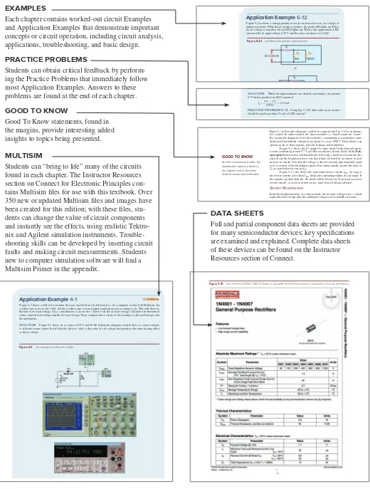
Figure 3-15 Data sheet for 1N4001–1N4007 diodes. (Copyright Fairchild Semiconductor Corporation. Used by permission.) EXAMPLES
Each chapter contains worked-out circuit Examples and Application Examples that demonstrate important concepts or circuit operation, including circuit analysis, applications, troubleshooting, and basic design.
Application Example 5-12
Figure 5-22a shows a voltage-polarity tester. It can be used to test a dc voltage of unknown polarity. When the dc voltage is positive, the green LED lights up. When the dc voltage is negative, the red LED lights up. What is the approximate LED current if the dc input voltage is 50 V and the series resistance is 2.2 kV?
RS
and switches. How much LED current is there if the series resistance is 470 V? SOLUTION When the input terminals are shorted (continuity), the internal 9-V battery produces an LED current of:
IS5 9 V _________ 2 2 V
470 V 5 14.9 mA
PRACTICE PROBLEM 5-13 Using Fig. 5-22b, what value series resistor should be used to produce 21 mA of LED current?
Application Example4-1
Figure 4-3 shows a half-wave rectifi er that you can build on the lab bench or on a computer screen with Multisim. An oscilloscope is across the 1 kV. Set the oscilloscope’s vertical input coupling switch or setting to dc. This will show us the half-wave load voltage. Also, a multimeter is across the 1 kV to read the dc load voltage. Calculate the theoretical values of peak load voltage and the dc load voltage. Then, compare these values to the readings on the oscilloscope and the multimeter.
SOLUTION Figure 4-3 shows an ac source of 10 V and 60 Hz. Schematic diagrams usually show ac source voltages as effective or rms values. Recall that the effective value is the value of a dc voltage that produces the same heating effect as the ac voltage.
Figure 4-3 Lab example of half-wave rectifi er. GOOD TO KNOW
Good To Know statements, found in the margins, provide interesting added insights to topics being presented.
p
Figure 5-1a shows the schematic symbol of a zener diode; Fig. 5-1b is an alterna-tive symbol. In either symbol, the lines resemble a z, which stands for “zener.” By varying the doping level of silicon diodes, a manufacturer can produce zener diodes with breakdown voltages from about 2 to over 1000 V. These diodes can operate in any of three regions: forward, leakage, and breakdown.
Figure 5-1c shows the I-V graph of a zener diode. In the forward region, it starts conducting around 0.7 V, just like an ordinary silicon diode. In the leak-age region (between zero and breakdown), it has only a small reverse current. In a zener diode, the breakdown has a very sharp knee, followed by an almost vertical increase in current. Note that the voltage is almost constant, approximately equal to VZ over most of the breakdown region. Data sheets usually specify the value of VZ at a particular test current IZT.
Figure 5-1c also shows the maximum reverse current IZM. As long as the reverse current is less than IZM, the diode is operating within its safe range. If the current is greater than IZM, the diode will be destroyed. To prevent excessive reverse current, a current-limiting resistor must be used (discussed later).
Zener Resistance
In the third approximation of a silicon diode, the forward voltage across a diode equals the knee voltage plus the additional voltage across the bulk resistance.
GOOD TO KNOW As with conventional diodes, the manufacturer places a band on the cathode end of the zener diode for terminal identification.
PRACTICE PROBLEMS
Students can obtain critical feedback by perform-ing the Practice Problems that immediately follow most Application Examples. Answers to these problems are found at the end of each chapter.
MULTISIM
Students can “bring to life” many of the circuits found in each chapter. The Instructor Resources section on Connect for Electronic Principles con-tains Multisim fi les for use with this textbook. Over 350 new or updated Multisim fi les and images have been created for this edition; with these fi les, stu-dents can change the value of circuit components and instantly see the effects, using realistic Tektro-nix and Agilent simulation instruments. Trouble-shooting skills can be developed by inserting circuit faults and making circuit measurements. Students new to computer simulation software will fi nd a Multisim Primer in the appendix.
DATA SHEETS
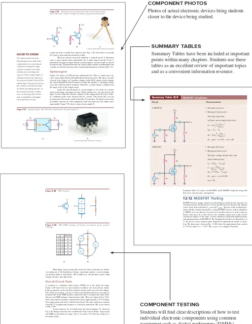
COMPONENT PHOTOS
Photos of actual electronic devices bring students closer to the device being studied.
SUMMARY TABLES
Summary Tables have been included at important points within many chapters. Students use these tables as an excellent review of important topics and as a convenient information resource.
COMPONENT TESTING
Students will fi nd clear descriptions of how to test individual electronic components using common equipment such as digital multimeters (DMMs).
Many things can go wrong with a transistor. Since it contains two diodes, exceeding any of the breakdown voltages, maximum currents, or power ratings can damage either or both diodes. The troubles may include shorts, opens, high leakage currents, and reduced dc.
Out-of-Circuit Tests
A transistor is commonly tested using a DMM set to the diode test range. Figure 6-28 shows how an npn transistor resembles two back-to-back diodes. Each pn junction can be tested for normal forward- and reverse-biased readings. The collector to emitter can also be tested and should result in an overrange in-dication with either DMM polarity connection. Since a transistor has three leads, there are six DMM polarity connections possible. These are shown in Fig. 6-29a. Notice that only two polarity connections result in approximately a 0.7 V reading. Also important to note here is that the base lead is the only connection common to both 0.7 V readings and it requires a (+) polarity connection. This is also shown in Fig. 6-29b.
A pnp transistor can be tested using the same technique. As shown in Fig. 6-30, the pnp transistor also resembles two back-to-back diodes. Again, using the DMM in the diode test range, Fig. 6-31a and 6-31b show the results for a normal tra nsistor.
⫽
Summary Table 12-5 shows a D-MOSFET and E-MOSFET amplifi er along with their basic characteristics and equations.
12-12 MOSFET Testing
MOSFET devices require special care when being tested for proper operation. As stated previously, the thin layer of silicon dioxide between the gate and channel can be easily destroyed when VGS exceeds VGS(max). Because of the insulated gate, along with the channel construction, testing MOSFET devices with an ohmmeter or DMM is not very effective. A good way to test these devices is with a semicon-ductor curve tracer. If a curve tracer is not available, special test circuits can be constructed. Figure 12-48a shows a circuit capable of testing both depletion-mode and enhancement-mode MOSFETs. By changing the voltage level and polarity of V1, the device can be tested in either depletion or enhancement modes of opera-tion. The drain curve shown in Fig. 12-48b shows the approximate drain current of 275 mA when VGS 5 4.52 V. The y-axis is set to display 50 mA/div.
Summary Table 12-5 MOSFET Amplifi ers Circuit Characteristics
• Normally on device.
• Biasing methods used: Zero-bias, gate-bias,
self-bias, and voltage-divider bias
ID 5 IDSS1 1 — 2VGS
• Biasing methods used: Gatebias, voltage-divider bias, and
drain-feedback bias
sensitivity with a variable base return resistor (Fig. 7-8b), but the base is usually left open to get maximum sensitivity to light.
The price paid for increased sensitivity is reduced speed. A phototran-sistor is more sensitive than a photodiode, but it cannot turn on and off as fast. A photodiode has typical output currents in microamperes and can switch on and off in nanoseconds. The phototransistor has typical output currents in milliamperes but switches on and off in microseconds. A typical phototransistor is shown in Fig. 7-8c.
Optocoupler
Figure 7-9a shows an LED driving a phototransistor. This is a much more sen-sitive optocoupler than the LED-photodiode discussed earlier. The idea is straight-forward. Any changes in VS produce changes in the LED current, which changes the current through the phototransistor. In turn, this produces a changing voltage across the collector-emitter terminals. Therefore, a signal voltage is coupled from the input circuit to the output circuit.
Again, the big advantage of an optocoupler is the electrical isolation between the input and output circuits. Stated another way, the common for the input circuit is different from the common for the output circuit. Because of this, no conductive path exists between the two circuits. This means that you can ground one of the circuits and fl oat the other. For instance, the input circuit can be grounded to the chassis of the equipment, while the common of the output side is ungrounded. Figure 7-9b shows a typical optocoupler IC.
(a)
© Brian Moeskau/Brian Moeskau Photography
Figure 7-8 Phototransistor. (a) Open base gives maximum sensitivity; (b) variable base resistor changes sensitivity; (c) typical phototransistor.
RC
© Brian Moeskau/Brian Moeskau Photography
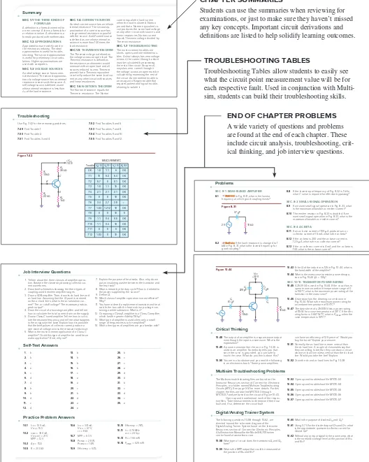
xiv Guided Tour formula produced with mathematics. SEC. 1-2 APPROXIMATIONS Approximations are widely used in the electronics industry. The ideal approximation is useful for trouble-shooting. The second approximation is useful for preliminary circuit calcu-lations. Higher approximations are used with computers. SEC. 1-3 VOLTAGE SOURCES An ideal voltage source has no inter-nal resistance. The second approxima-tion of a voltage source has an internal resistance in series with the source. A stiff voltage source is defi ned as one whose internal resistance is less than 1⁄100 of the load resistance.
SEC. 1-4 CURRENT SOURCES An ideal current source has an infi nite internal resistance. The second ap-proximation of a current source has a large internal resistance in parallel with the source. A stiff current source is defi ned as one whose internal re-sistance is more than 100 times the load resistance.
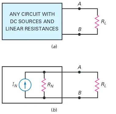
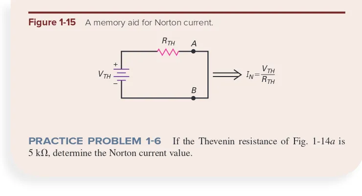
SEC. 1-5 THEVENIN’S THEOREM The Thevenin voltage is defi ned as the voltage across an open load. The Thevenin resistance is defi ned as the resistance an ohmmeter would measure with an open load and all sources reduced to zero. Thevenin proved that a Thevenin equivalent circuit will produce the same load cur-rent as any other circuit with sources and linear resistances. SEC. 1-6 NORTON’S THEOREM The Norton resistance equals the Thevenin resistance. The Norton
current equals the load current when the load is shorted. Norton proved that a Norton equivalent cir-cuit produces the same load voltage as any other circuit with sources and linear resistances. Norton current equals Thevenin voltage divided by Thevenin resistance. SEC. 1-7 TROUBLESHOOTING The most common troubles are shorts, opens, and intermittent trou-bles. A short always has zero voltage across it; the current through a short must be calculated by examining the rest of the circuit. An open al-ways has zero current through it; the voltage across an open must be calculated by examining the rest of the circuit. An intermittent trouble is an on-again, off -again trouble that requires patient and logical trouble-shooting to isolate it.
Troubleshooting
Use Fig. 7-42 for the remaining problems.
7-49 Find Trouble 1.
SEC. 8-1 BASE-BIASED AMPLIFIER 8-1 In Fig. 8-31, what is the lowest
frequency at which good coupling exists?
8-8 If the lowest input frequency of Fig. 8-32 is 1 kHz, what C value is required for eff ective bypassing? SEC. 8-3 SMALL-SIGNAL OPERATION 8-9 If we want small-signal operation in Fig. 8-33, what
is the maximum allowable ac emitter current?
8-10 The emitter resistor in Fig. 8-33 is doubled. If we want small-signal operation in Fig. 8-33, what is the maximum allowable ac emitter current? SEC. 8-4 AC BETA
8-11 If an ac base current of 100 A produces an ac collector current of 15 mA, what is the ac beta?
8-12 If the ac beta is 200 and the ac base current is 12.5 A, what is the ac collector current?
8-13 If the ac collector current is 4 mA and the ac beta is 100, what is the ac base current? 2 V 10 kΩ
47 mF Figure 8-31
8-2 If the load resistance is changed to 1 kV in Fig. 8-31, what is the lowest frequency for good coupling?
CHAPTER SUMMARIES
Students can use the summaries when reviewing for examinations, or just to make sure they haven’t missed any key concepts. Important circuit derivations and defi nitions are listed to help solidify learning outcomes.
TROUBLESHOOTING TABLES
Troubleshooting Tables allow students to easily see what the circuit point measurement value will be for each respective fault. Used in conjunction with Multi-sim, students can build their troubleshooting skills.
END OF CHAPTER PROBLEMS
A wide variety of questions and problems are found at the end of each chapter. These include circuit analysis, troubleshooting, crit-ical thinking, and job interview questions.
10-43 If the Q of the inductor is 125 in Fig. 10-44, what is the bandwidth of the amplifi er?
10-44 What is the worst-case transistor power dissipa-tion in Fig. 10-44 (Q 5 125)? SEC. 10-10 TRANSISTOR POWER RATING 10-45 A 2N3904 is used in Fig. 10-44. If the circuit has to
operate over an ambient temperature range of 0 to 100°C, what is the maximum power rating of the transistor in the worst case?
10-46 A transistor has the derating curve shown in Fig. 10-34. What is the maximum power rating for an ambient temperature of 100°C?
10-47 The data sheet of a 2N3055 lists a power rating of 115 W for a case temperature of 25°C. If the der-ating factor is 0.657 W/°C, what is PD(max) when the case temperature is 90°C?
R1
10-48 The output of an amplifi er is a square-wave output even though the input is a sine wave. What is the explanation?
10-49 A power transistor like the one in Fig. 10-36 is used in an amplifi er. Somebody tells you that since the case is grounded, you can safely touch the case. What do you think about this?
10-50 You are in a bookstore and you read the following in an electronics book: “Some power amplifi ers
can have an effi ciency of 125 percent.” Would you buy the book? Explain your answer.
10-51 Normally, the ac load line is more vertical than the dc load line. A couple of classmates say that they are willing to bet that they can draw a circuit whose ac load line is less vertical than the dc load line. Would you take the bet? Explain.
10-52 Draw the dc and ac load lines for Fig. 10-38.
Multisim Troubleshooting Problems
The Multisim troubleshooting fi les are found on the Instructor Resources section of Connect for Electronic Principles, in a folder named Multisim Troubleshooting Circuits (MTC). See page XVI for more details. For this chapter, the fi les are labeled MTC10-53 through MTC10-57 and are based on the circuit of Figure 10-43.
Open up and troubleshoot each of the respec-tive fi les. Take measurements to determine if there is a fault and, if so, determine the circuit fault.
10-53 Open up and troubleshoot fi le MTC10-53.
10-54 Open up and troubleshoot fi le MTC10-54.
10-55 Open up and troubleshoot fi le MTC10-55.
10-56 Open up and troubleshoot fi le MTC10-56.
10-57 Open up and troubleshoot fi le MTC10-57.
Digital/Analog Trainer System
The following questions, 10-58 through 10-62, are directed toward the schematic diagram of the Digital/Analog Trainer System found on the Instructor Resources section of Connect for Electronic Principles. A full Instruction Manual for the Model XK-700 trainer can be found at www.elenco.com.
10-58 What type of circuit does the transistors Q1 and Q2 form?
10-59 What is the MPP output that could be measured at the junction of R46 and R47?
10-60 What is the purpose of diodes D16 and D17?
10-61 Using 0.7 V for the diode drops of D16 and D17, what is the approximate quiescent collector current for Q1 and Q2?
10-62 Without any ac input signal to the power amp, what is the normal dc voltage level at the junction of R46 and R47?
Job Interview Questions
1. Tell me about the three classes of amplifi er opera-tion. Illustrate the classes by drawing collector cur-rent waveforms.
2. Draw brief schematics showing the three types of coupling used between amplifi er stages. 3. Draw a VDB amplifi er. Then, draw its dc load line and
ac load line. Assuming that the Q point is centered on the ac load lines, what is the ac saturation cur-rent? The ac cutoff voltage? The maximum peak-to-peak output?
4. Draw the circuit of a two-stage amplifi er and tell me how to calculate the total current drain on the supply. 5. Draw a Class-C tuned amplifi er. Tell me how to
calcu-late the resonant frequency, and tell me what happens to the ac signal at the base. Explain how it is possible that the brief pulses of collector current produce a sine wave of voltage across the resonant tank circuit. 6. What is the most common application of a Class-C
amplifi er? Could this type of amplifi er be used for an audio application? If not, why not?
7. Explain the purpose of heat sinks. Also, why do we put an insulating washer between the transistor and the heat sink?
8. What is meant by the duty cycle? How is it related to the power supplied by the source? 9. Defi ne Q.
10. Which class of amplifi er operation is most effi cient? Why?
11. You have ordered a replacement transistor and heat sink. In the box with the heat sink is a package con-taining a white substance. What is it? 12. Comparing a Class-A amplifi er to a Class-C amplifi er,
which has the greater fi delity? Why? 13. What type of amplifi er is used when only a small
range of frequencies is to be amplifi ed? 14. What other types of amplifi ers are you familiar with?
Student
Resources
In addition to the fully updated text, a number of student learning resources have been developed to aid readers in their understanding of electronic principles and applications.
• The online resources for this edition include McGraw-Hill Connect®,
a web-based assignment and assessment platform that can help students to perform better in their coursework and to master important concepts.
With Connect®, instructors can deliver assignments, quizzes, and tests
easily online. Students can practice important skills at their own pace and on their own schedule. Ask your McGraw-Hill representative for more detail and check it out at www.mcgrawhillconnect.com.
• McGraw-Hill LearnSmart® is an adaptive learning system designed
to help students learn faster, study more effi ciently, and retain more knowledge for greater success. Through a series of adaptive questions,
Learnsmart® pinpoints concepts the student does not understand and
maps out a personalized study plan for success. It also lets instructors see exactly what students have accomplished, and it features a built-in assessment tool for graded assignments. Ask your McGraw-Hill repre-sentative for more information, and visit www.mhlearnsmart.com for a demonstration.
• Fueled by LearnSmart—the most widely used and intelligent adaptive
learning resource—SmartBook® is the fi rst and only adaptive reading
experience available today.
Distinguishing what a student knows from what they don’t, and honing in on concepts they are most likely to forget, SmartBook personalizes content for each student in a continuously adapting reading experience. Reading is no longer a passive and linear experience, but an engaging and dynamic one where students are more likely to master and retain important concepts, coming to class better prepared. Valuable reports provide instructors insight as to how students are progressing through textbook content, and are useful for shaping in-class time or assessment.
As a result of the adaptive reading experience found in SmartBook, students are more likely to retain knowledge, stay in class and get better grades.
This revolutionary technology is available only from McGraw-Hill Education and for hundreds of course areas as part of the LearnSmart Advantage series.
xvi
Instructor
Resources
• Instructor’s Manual provides solutions and teaching suggestions for the text and Experiments Manual.
• PowerPoint slides for all chapters in the text, and Electronic Test-banks with additional review questions for each chapter can be found on the Instructor Resources section on Connect.
• Experiments Manual, for Electronic Principles, correlated to the textbook, with lab follow-up information included on the Instructor Resources section on Connect.
Directions for accessing the Instructor Resources through Connect
To access the Instructor Resources through Connect, you must fi rst con-tact your McGraw-Hill Learning Technology Representative to obtain a password. If you do not know your McGraw-Hill representative, please go to www.mhhe.com/rep, to fi nd your representative.
Once you have your password, please go to connect.mheducation.com,
and login. Click on the course for which you are using Electronic Principles. If you
have not added a course, click “Add Course,” and select “Engineering
Technol-ogy” from the drop-down menu. Select Electronic Principles, 8e and click “Next.”
Acknowledgments
The production of Electronic Principles, eighth edition, involves the combined
effort of a team of professionals.
Thank you to everyone at McGraw-Hill Higher Education who contrib-uted to this edition, especially Raghu Srinivasan, Vincent Bradshaw, Jessica Portz, and Vivek Khandelwal. Special thanks go out to Pat Hoppe whose insights and tremendous work on the Multisim fi les has been a signifi cant contribution to this textbook. Thanks to everyone whose comments and suggestions were extremely valuable in the development of this edition. This includes those who took the time to respond to surveys prior to manuscript development and those who carefully reviewed the revised material. Every survey and review were carefully examined and have contributed greatly to this edition. In this edition, valuable input was obtained from electronics instructors from across the country and international reviewers. Also, reviews and input from electronics certifi cation organizations,
including CertTEC, ETA International, ISCET, and NCEE, were very benefi cial.
Here is a list of the reviewers who helped make this edition comprehensive and relevant.
Current Edition Reviewers
Reza Chitsazzadeh
Community College of Allegheny County
Walter Craig
Southern University and A&M College
Abraham Falsafi
BridgeValley Community & Technical College
Robert Folmar
Brevard Community College Robert Hudson
Southern University at Shreveport Louisiana
John Poelma
Mississippi Gulf Coast Community College
Chueh Ting
New Mexico State University John Veitch
SUNY Adirondack KG Bhole
University of Mumbai Pete Rattigan
President
International Society of Certifi ed Electronics Technicians Steve Gelman
2
chapter
1
Introduction
This important chapter serves as a framework for the rest
of the textbook. The topics in this chapter include formulas,
voltage sources, current sources, two circuit theorems, and
troubleshooting. Although some of the discussion will be review,
you will fi nd new ideas, such as circuit approximations, that can
make it easier for you to understand semiconductor devices.
cold-solder joint defi nition derivation duality principle formula
ideal (fi rst) approximation law
Norton current Norton resistance open device
second approximation shorted device
solder bridge stiff current source
stiff voltage source theorem
Thevenin resistance Thevenin voltage third approximation troubleshooting
Vocabulary
bchob_ha
bchop_ha
bchop_ln
Objectives
After studying this chapter, you should be able to:
■ Name the three types of formulas
and explain why each is true.
■ Explain why approximations
are often used instead of exact formulas.
■ Defi ne an ideal voltage source
and an ideal current source.
■ Describe how to recognize a stiff
voltage source and a stiff current source.
■ State Thevenin’s theorem and
apply it to a circuit.
■ State Norton’s theorem and
apply it to a circuit.
■ List two facts about an open
device and two facts about a shorted device.
bchop_haa
Chapter Outline
1-1 The Three Kinds of Formulas
1-2 Approximations
1-3 Voltage Sources
1-4 Current Sources
1-5 Thevenin’s Theorem
1-6 Norton’s Theorem
4 Chapter 1
1-1
The Three Kinds of Formulas
A formula is a rule that relates quantities. The rule may be an equation, an in-equality, or other mathematical description. You will see many formulas in this book. Unless you know why each one is true, you may become confused as they accumulate. Fortunately, there are only three ways formulas can come into existence. Knowing what they are will make your study of electronics more logical and satisfying.
The Defi nition
When you study electricity and electronics, you have to memorize new words like
current, voltage, and resistance. However, a verbal explanation of these words is not enough. Why? Because your idea of current must be mathematically identical
to everyone else’s. The only way to get this identity is with a defi nition, a formula
invented for a new concept.
Here is an example of a defi nition. In your earlier course work, you learned that capacitance equals the charge on one plate divided by the voltage between plates. The formula looks like this:
C 5 __QV
This formula is a defi nition. It tells you what capacitance C is and how to
calcu-late it. Historically, some researcher made up this defi nition and it became widely accepted.
Here is an example of how to create a new defi nition out of thin air. Suppose we are doing research on reading skills and need some way to measure
reading speed. Out of the blue, we might decide to defi ne reading speed as the
number of words read in a minute. If the number of words is W and the number of
minutes is M, we could make up a formula like this:
S 5 __WM
In this equation, S is the speed measured in words per minute.
To be fancy, we could use Greek letters: for words, for minutes, and
for speed. Our defi nition would then look like this:
5 __
This equation still translates to speed equals words divided by minutes. When you see an equation like this and know that it is a defi nition, it is no longer as impres-sive and mysterious as it initially appears to be.
In summary, defi nitions are formulas that a researcher creates. They are
based on scientifi c observation and form the basis for the study of electronics. They are simply accepted as facts. It’s done all the time in science. A defi nition is true in the same sense that a word is true. Each represents something we want to talk about. When you know which formulas are defi nitions, electronics is easier to understand. Because defi nitions are starting points, all you need to do is under-stand and memorize them.
The Law
A law is different. It summarizes a relationship that already exists in nature. Here
is an example of a law:
f 5 K _____ Q1Q2
d2
GOOD TO KNOW
where f 5 force
K 5 a constant of proportionality, 9(109)
Q1 5 fi rst charge
Q2 5 second charge
d 5 distance between charges
This is Coulomb’s law. It says that the force of attraction or repulsion between two charges is directly proportional to the charges and inversely proportional to the square of the distance between them.
This is an important equation, for it is the foundation of electricity. But where does it come from? And why is it true? To begin with, all the variables in this law existed before its discovery. Through experiments, Coulomb was able to prove that the force was directly proportional to each charge and inversely pro-portional to the square of the distance between the charges. Coulomb’s law is an example of a relationship that exists in nature. Although earlier researchers could
measure f, Q1, Q2, and d, Coulomb discovered the law relating the quantities and
wrote a formula for it.
Before discovering a law, someone may have a hunch that such a rela-tionship exists. After a number of experiments, the researcher writes a formula that summarizes the discovery. When enough people confi rm the discovery
through experiments, the formula becomes a law. A law is true because you can
verify it with an experiment.
The Derivation
Given an equation like this:
y 5 3x
we can add 5 to both sides to get:
y 1 5 5 3x 1 5
The new equation is true because both sides are still equal. There are many other operations like subtraction, multiplication, division, factoring, and substitution that preserve the equality of both sides of the equation. For this reason, we can derive many new formulas using mathematics.
A derivation is a formula that we can get from other formulas. This means that we start with one or more formulas and, using mathematics, arrive at a new formula not in our original set of formulas. A derivation is true because mathematics preserves the equality of both sides of every equation between the starting formula and the derived formula.
For instance, Ohm was experimenting with conductors. He discovered
that the ratio of voltage to current was a constant. He named this constant
resis-tance and wrote the following formula for it:
R 5 __VI
This is the original form of Ohm’s law. By rearranging it, we can get:
I 5 __VR
6 Chapter 1
Here is another example. The defi nition for capacitance is:
C 5 __ Q
V
We can multiply both sides by V to get the following new equation:
Q 5 CV
This is a derivation. It says that the charge on a capacitor equals its capacitance times the voltage across it.
What to Remember
Why is a formula true? There are three possible answers. To build your under-standing of electronics on solid ground, classify each new formula in one of these three categories:
Defi nition: A formula invented for a new concept
Law:A formula for a relationship in nature
Derivation:A formula produced with mathematics
1-2
Approximations
We use approximations all the time in everyday life. If someone asks you how old you are, you might answer 21 (ideal). Or you might say 21 going on 22 (second approximation). Or, maybe, 21 years and 9 months (third approximation). Or, if you want to be more accurate, 21 years, 9 months, 2 days, 6 hours, 23 minutes, and 42 seconds (exact).
The foregoing illustrates different levels of approximation: an ideal ap-proximation, a second apap-proximation, a third apap-proximation, and an exact answer. The approximation to use will depend on the situation. The same is true in elec-tronics work. In circuit analysis, we need to choose an approximation that fi ts the situation.
The Ideal Approximation
Did you know that 1 foot of AWG 22 wire that is 1 inch from a chassis has a
resistance of 0.016 V, an inductance of 0.24 H, and a capacitance of 3.3 pF? If
we had to include the effects of resistance, inductance, and capacitance in every calculation for current, we would spend too much time on calculations. This is why everybody ignores the resistance, inductance, and capacitance of connecting wires in most situations.
The ideal approximation, sometimes called the fi rst approximation, is
the simplest equivalent circuit for a device. For instance, the ideal approximation of a piece of wire is a conductor of zero resistance. This ideal approximation is adequate for everyday electronics work.
The exception occurs at higher frequencies, where you have to con-sider the inductance and capacitance of the wire. Suppose 1 inch of wire has an
inductance of 0.24 H and a capacitance of 3.3 pF. At 10 MHz, the inductive
reactance is 15.1 V, and the capacitive reactance is 4.82 kV. As you see, a
As a guideline, we can idealize a piece of wire at frequencies under 1 MHz. This is usually a safe rule of thumb. But it does not mean that you can be careless about wiring. In general, keep connecting wires as short as possible, because at some point on the frequency scale, those wires will begin to degrade circuit performance.
When you are troubleshooting, the ideal approximation is usually adequate because you are looking for large deviations from normal voltages and currents. In this book, we will idealize semiconductor devices by reducing them to simple equiv-alent circuits. With ideal approximations, it is easier to analyze and understand how semiconductor circuits work.
The Second Approximation
The ideal approximation of a fl ashlight battery is a voltage source of 1.5 V. The
second approximation adds one or more components to the ideal approximation. For instance, the second approximation of a fl ashlight battery is a voltage source of
1.5 V and a series resistance of 1 V. This series resistance is called the source or
internal resistance of the battery. If the load resistance is less than 10 V, the load volt-age will be noticeably less than 1.5 V because of the voltvolt-age drop across the source resistance. In this case, accurate calculations must include the source resistance.
The Third Approximation and Beyond
The third approximation includes another component in the equivalent circuit of the device. An example of the third approximation will be examined when we discuss semiconductor diodes.
Even higher approximations are possible with many components in the equivalent circuit of a device. Hand calculations using these higher approxima-tions can become diffi cult and time consuming. Because of this, computers using circuit simulation software are often used. For instance, Multisim by National Instruments (NI) and PSpice are commercially available computer programs that use higher approximations to analyze and simulate semiconductor circuits. Many of the circuits and examples in this book can be analyzed and demonstrated using this type of software.
Conclusion
Which approximation to use depends on what you are trying to do. If you are troubleshooting, the ideal approximation is usually adequate. For many situations, the second approximation is the best choice because it is easy to use and does not require a computer. For higher approximations, you should use a computer and a program like Multisim. A Multisim tutorial can be found on the Instructor
Resources section of Connect for Electronic Principles.
1-3
Voltage Sources
An ideal dc voltage source produces a load voltage that is constant. The sim-plest example of an ideal dc voltage source is a perfect battery, one whose
inter-nal resistance is zero. Figure 1-1a shows an ideal voltage source connected to a
variable load resistance of 1 V to 10 MV. The voltmeter reads 10 V, exactly the
same as the source voltage.
Figure 1-1b shows a graph of load voltage versus load resistance. As you
can see, the load voltage remains fi xed at 10 V when the load resistance changes
from 1 V to 1 MV. In other words, an ideal dc voltage source produces a constant
8 Chapter 1
Second Approximation
An ideal voltage source is a theoretical device; it cannot exist in nature. Why? When the load resistance approaches zero, the load current approaches infi nity. No real voltage source can produce infi nite current because a real voltage source always has some internal resistance. The second approximation of a dc voltage source includes this internal resistance.
Figure 1-2a illustrates the idea. A source resistance RS of 1 V is now in
series with the ideal battery. The voltmeter reads 5 V when RL is 1 V. Why?
Be-cause the load current is 10 V divided by 2 V, or 5 A. When 5 A fl ows through the
source resistance of 1 V, it produces an internal voltage drop of 5 V. This is why
the load voltage is only half of the ideal value, with the other half being dropped across the internal resistance.
Figure 1-2b shows the graph of load voltage versus load resistance. In
this case, the load voltage does not come close to the ideal value until the load
resistance is much greater than the source resistance. But what does much greater
mean? In other words, when can we ignore the source resistance?
Figure 1-1 (a) Ideal voltage source and variable load resistance; (b) load voltage is constant for all load resistances.
(a) VS
10 V
RL
1 Ω–1 MΩ M1
10.0 V
7 8 9 10 11
1M
1 100 1k 10k 100k
(b)
RL resistance (Ohms) VS (V)
– +
Figure 1-2 (a) Second approximation includes source resistance; (b) load voltage is constant for large load resistances.
4 5 6 7 8 9 10
1M
1 100 1k 10k 100k
Stiff region
(b)
RL resistance (Ohms)
VS (V)
(a) RL
1 Ω–1 MΩ RS
1 Ω
M1 VS
10 V – 5.0 V
Stiff Voltage Source
Now is the time when a new defi nition can be useful. So, let us invent one. We can ignore the source resistance when it is at least 100 times smaller than the load
resistance. Any source that satisfi es this condition is a stiff voltage source. As a
defi nition,
Stiff voltage source:RS , 0.01RL (1-1)
This formula defi nes what we mean by a stiff voltage source. The boundary of the
inequality (where , is changed to 5) gives us the following equation:
RS 5 0.01RL
Solving for load resistance gives the minimum load resistance we can use and still have a stiff source:
RL(min)5100RS (1-2)
In words, the minimum load resistance equals 100 times the source resistance. Equation (1-2) is a derivation. We started with the defi nition of a stiff voltage source and rearranged it to get the minimum load resistance permitted
with a stiff voltage source. As long as the load resistance is greater than 100RS, the
voltage source is stiff. When the load resistance equals this worst-case value, the calculation error from ignoring the source resistance is 1 percent, small enough to ignore in a second approximation.
Figure 1-3 visually summarizes a stiff voltage source. The load
resis-tance has to be greater than 100RS for the voltage source to be stiff.
Figure 1-3 Stiff region occurs when load resistance is large enough.
100Rs
Stiff region
RL resistance (Ohms)
VS (V)
GOOD TO KNOW
A well-regulated power supply is a good example of a stiff voltage source.
Example
1-1
The defi nition of a stiff voltage source applies to ac sources as well as to dc
sources. Suppose an ac voltage source has a source resistance of 50 V. For what
load resistance is the source stiff?
SOLUTION Multiply by 100 to get the minimum load resistance:
10 Chapter 1
1-4
Current Sources
A dc voltage source produces a constant load voltage for different load
resis-tances. A dc current source is different. It produces a constant load current for
different load resistances. An example of a dc current source is a battery with a
large source resistance (Fig. 1-4a). In this circuit, the source resistance is 1 MV
and the load current is:
IL 5
VS
_______ RS 1 RL
When RL is 1 V in Fig. 1-4a, the load current is:
IL 5 ____________1 MV 10 V1 1 V 5 10 A
In this calculation, the small load resistance has an insignifi cant effect on the load current.
Figure 1-4b shows the effect of varying the load resistance from 1 V to
1 MV. In this case, the load current remains constant at 10 A over a large range.
It is only when the load resistance is greater than 10 kV that a noticeable drop-off
occurs in load current.
As long as the load resistance is greater than 5 kV, the ac voltage source is stiff
and we can ignore the internal resistance of the source.
A fi nal point. Using the second approximation for an ac voltage source
is valid only at low frequencies. At high frequencies, additional factors such as
lead inductance and stray capacitance come into play. We will deal with these high-frequency effects in a later chapter.
PRACTICE PROBLEM 1-1 If the ac source resistance in Example 1-1 is
600 V, for what load resistance is the source stiff?
GOOD TO KNOW
At the output terminals of a constant current source, the load voltage VL increases in direct proportion to the load resistance.
Figure 1-4 (a) Simulated current source with a dc voltage source and a large resistance; (b) load current is constant for small load resistances.
(a)
M1 RL
1 Ω–1 MΩ RS
1 MΩ
VS
10 V
4 5 6 7 8 9 10
1M
1 100 1k 10k 100k
Stiff region
(b)
RL resistance (Ohms)
IL ( A)µ
10.0 Aµ –
Stiff Current Source
Here is another defi nition that will be useful, especially with semiconductor cir-cuits. We will ignore the source resistance of a current source when it is at least 100 times larger than the load resistance. Any source that satisfi es this condition
is a stiff current source. As a defi nition:
Stiff current source: RS . 100RL (1-3)
The upper boundary is the worst case. At this point:
RS 5 100RL
Solving for load resistance gives the maximum load resistance we can use and still have a stiff current source:
RL(max)50.01RS (1-4)
In words: The maximum load resistance equals 1⁄
100 of the source resistance.
Equation (1-4) is a derivation because we started with the defi nition of a stiff current source and rearranged it to get the maximum load resistance. When the load resistance equals this worst-case value, the calculation error is 1 percent, small enough to ignore in a second approximation.
Figure 1-5 shows the stiff region. As long as the load resistance is less
than 0.01RS, the current source is stiff.
Schematic Symbol
Figure 1-6a is the schematic symbol of an ideal current source, one whose source
resistance is infi nite. This ideal approximation cannot exist in nature, but it can exist mathematically. Therefore, we can use the ideal current source for fast circuit analysis, as in troubleshooting.
Figure 1-6a is a visual defi nition: It is the symbol for a current source.
When you see this symbol, it means that the device produces a constant current IS.
It may help to think of a current source as a pump that pushes out a fi xed number of coulombs per second. This is why you will hear expressions like “The current
source pumps 5 mA through a load resistance of 1 kV.”
Figure 1-6b shows the second approximation. The internal resistance
is in parallel with the ideal current source, not in series as it was with an ideal voltage source. Later in this chapter we will discuss Norton’s theorem. You will then see why the internal resistance must be in parallel with the current source. Summary Table 1-1 will help you understand the differences between a voltage source and a current source.
Figure 1-5 Stiff region occurs when load resistance is small enough.
0.01RS
100%
99%
Load resistance
Load current
Stiff region
Figure 1-6 (a) Schematic symbol of a current source; (b) second approximation of a current source.
RS
IS IS
12 Chapter 1
Summary Table 1-1
Properties of Voltage and
Current Sources
Quantity Voltage Source Current Source
R S Typically low Typically high
R L Greater than 100 R S Less than 0.01 R S
V L Constant Depends on R L
I L Depends on R L Constant
Example
1-2
A current source of 2 mA has an internal resistance of 10 MV. Over what range of load resistance is the current source stiff?
SOLUTION Since this is a current source, the load resistance has to be small compared to the source resistance. With the 100:1 rule, the maximum load resistance is:
RL(max) 5 0.01(10 MV) 5 100 kV
The stiff range for the current source is a load resistance from 0 to 100 kV.
Figure 1-7 summarizes the solution. In Fig. 1-7a, a current source of 2 mA is in parallel with 10 MV and a variable
resistor set to 1 V. The ammeter measures a load current of 2 mA. When the load resistance changes from 1 V to 1 MV, as
shown in Fig. 1-7b, the source remains stiff up to 100 kV. At this point, the load current is down about 1 percent from the
ideal value. Stated another way, 99 percent of the source current passes through the load resistance. The other 1 percent passes through the source resistance. As the load resistance continues to increase, load current continues to decrease.
PRACTICE PROBLEM 1-2 What is the load voltage in Fig. 1-7a when the load resistance equals 10 kV?
Figure 1-7 Solution.
(a)
2.0 mA
RL
1 Ω–10 MΩ RS
10 MΩ IS
2 mA
1.80 1.85 1.90 1.95 2.00
1M
1 100 1k 10k 100k
Stiff region
(b)
RL resistance (Ohms)