ABSTRAK
Kemajuan ilmu teknologi semakin pesat setiap hari termasuk bidang
Robotika. Robot semakin beraneka ragam bentuk dan fungsinya. Contohnya
Mobile Robot yang dilengkapi dengan roda, digerakkan dengan sumber tenaga
baterai dan diarahkan dari jarak jauh. Mobile Robot dapat juga beroperasi melalui
Mikrokontroler yang sudah diprogram terlebih dahulu. Di Indonesia
perkembangan robotika ditandai dengan adanya KRCI (Kontes Robot Cerdas
Indonesia) dan kontes lain seperti Lomba Robot Line Follower yang diadakan di
ITB maret 2007 nanti.
Pada Tugas Akhir ini telah direalisasikan robot bergerak menghindari
rintangan dan mendeteksi sumber cahaya sebagai titik tujuan. Robot dilengkapi
dengan tiga buah sensor infrared untuk mengetahui keberadaan rintangan. Sensor
intensitas cahaya berupa LDR (Light Dependent Resistor) akan mencari sumber
cahaya sebagai titik akhir yang akan dituju. Dua buah motor DC yang akan
menggerakkan robot berasal dari sebuah mobil mainan yang dimodifikasi.
Robot yang direalisasikan memiliki sensor infrared yang bekerja dengan
baik di ruangan yang mempunyai intensitas cahaya maksimal 40 Lux. Robot dapat
berhasil menghindari rintangan dengan percobaan mulai dari satu rintangan
sampai dengan tiga rintangan dan Robot juga berhasil bergerak menuju titik
tujuan berupa sumber cahaya dalam kondisi Robot tidak keluar dari lintasan.
Keberhasilan Robot ditentukan oleh faktor posisi rintangan, intensitas cahaya
ruangan dan posisi robot awal.
DAFTAR ISI
ABSTRAK ... ...i
ABSTRACT... ...ii
KATA PENGANTAR ... ...iii
DAFTAR ISI... ...v
DAFTAR TABEL... ...vii
DAFTAR GAMBAR ... ....viii
BAB I PENDAHULUAN ... 1
I.1
Latar belakang
... 1
I.2
Identifikasi Masalah
... 2
I.3
Tujuan
... 2
I.4
Pembatasan Masalah
... 2
I.4
Spesifikasi Alat
... 2
1.6
Sistematika Penulisan
... 3
BAB II LANDASAN TEORI ... 4
II.1 Mikrokontroler MCS-51... 4
II.1.1 Central Processing Unit (CPU) ... 6
II.1.2 Bagian Masukan/Keluaran (I/O, Input/Output)... 6
II.1.3 Organisasi Memori ... 7
II.1.3.1 Memori Program ... 7
II.1.3.2 Memori Data... 7
II.1.4 Koneksi Pin pada AT89S52 ... 8
II.1.5 Perangkat Lunak... 9
II.1.6 Interupsi... 10
II.2 Sensor... 11
II.3 Motor Arus Searah (DC) ... 16
II.5
ADC (Analog to Digital Converter) ... 18
II.6 Relay... 19
vi
BAB III PERANCANGAN ALAT... 20
III.1
Diagram Blok Robot dan Cara Kerja ... 20
III.2
Rangkaian Mikrokontroler AT89S52 ... 21
III.3
Rangkaian Sensor Kedekatan (optocoupler) untuk mendeteksi rintangan ...
... 24
III.4
Rangkaian Sensor Intensitas Cahaya (LDR) Untuk Mendeteksi Titik
Tujuan
Robot... 27
III.5
Rangkaian Relay dan Motor DC ... 29
III.6
Perancangan Perangkat Lunak ... 31
BAB IV DATA PENGAMATAN DAN ANALISA ... 33
IV.1
Pengujian Sensor Infra Merah... 33
IV.2
Pengujian Sensor Intensitas Cahaya LDR... 34
IV.3
Lintasan yang dilalui Robot ... 35
IV.3.1 Percobaan I... 35
IV.3.2 Percobaan II ... 38
IV.3.3 Percobaan III... 42
IV.3.4 Percobaan IV... 45
BAB V KESIMPULAN DAN SARAN... 49
V.1 Kesimpulan ... 49
V.2 Saran... 49
DAFTAR PUSTAKA...x
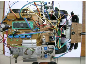
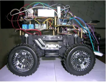
LAMPIRAN A FOTO ROBOT BERGERAK
DAFTAR TABEL
Tabel II.1 Alamat Layanan rutin interupsi...11
Tabel III.1 Gerakan kendaraan berdasarkan keluaran mikrokontroler ...31
Tabel IV.1 Tegangan Output Sensor Infrared...33
Tabel IV.2 Tegangan Output LDR untuk beberapa posisi derajat...34
Tabel IV.1 Tegangan Output Sensor Infrared...34
Tabel IV.2 Tegangan Output LDR untuk beberapa posisi derajat...35
Tabel IV.3 Hasil Percobaan I untuk posisi awal robot yang berbeda ...38
Tabel IV.4 Hasil percobaan sensor infrared yang mendeteksi satu rintangan ...41
Tabel IV.5 Hasil percobaan jika nilai X diubah...45
Tabel IV.6 Hasil percobaan jika nilai X dan Y diubah...48
DAFTAR GAMBAR
Gambar II.1 Arsitektur mikrokontroler ATMEL 89S52... 5
Gambar II.2 Memori data Internal ... 7
Gambar II.3 Mikrokontroler AT89S52 ... 8
Gambar II.4 Diagram Blok Sensor Optocoupler ... 12
Gambar II.5 Rangkaian Fotodioda... 13
Gambar II.6 Contoh LDR ... 14
Gambar II.7 Aplikasi LDR pada rangkaian ... 15
Gambar II.8 Grafik karakteristik LDR... 15
Gambar II.9 Cara kerja motor DC... 17
Gambar II.10 (a) Relay OFF (b) Relay ON ... 19
Gambar III.1 Diagram Blok Robot ... 21
Gambar III.2 Rangkaian Pembangkit Pulsa ... 21
Gambar III.3 Rangkaian manual reset ... 22
Gambar III.4 Rangkaian Mikrokontroler AT 89S52... 23
Gambar III.5 Rangkaian Transmitter... 24
Gambar III.6 Rangkaian Receiver... 24
Gambar III.7 Letak sensor pada Robot Bergerak... 26
Gambar III.8 Rangkaian Sensor LDR... 27
Gambar III.9 Rangkaian Penggerak Motor Stepper... 28
Gambar III.10 Letak Sensor LDR pada Motor Stepper ... 28
Gambar III.11 ADC0804 yang Self-Clocking dalam mode Free-Running... 28
Gambar III.12 Rangkaian Penggerak Relay dan Motor DC ... 29
Gambar III.13 Flowchart Program Utama... 31
Gambar III.14 Flowchart Subroutine Scan Cahaya... 32
Gambar III.15 Flowchart subroutine Robot belok kiri dan belok kanan... 32
ix
Gambar IV.1 Sudut posisi LDR terhadap sumber cahaya ... 34
Gambar IV.2 Robot bergerak dari titik awal... 36
Gambar IV.3 Robot menscan sumber cahaya ... 36
Gambar IV.4 Robot mendekati sumber cahaya ... 36
Gambar IV.5 Lintasan Robot untuk Percobaan I ... 37
Gambar IV.6 Lintasan Robot untuk percobaan I ... 37
Gambar IV.7 Robot bergerak dari titik awal... 38
Gambar IV.8 Robot mendeteksi rintangan... 39
Gambar IV.9 Robot mundur setelah mendeteksi rintangan ... 39
Gambar IV.10 Robot belok ke kiri untuk menghindari rintangan ... 39
Gambar IV.11 Titik tujuan yang akan dituju oleh robot... 40
Gambar IV.12 Robot menscan intensitas cahaya di sekitarnya ... 40
Gambar IV.13 Robot mendekati intensitas cahaya terbesar ... 40
Gambar IV.14 Gambar keseluruhan percobaan II ... 41
Gambar IV.15 Robot bergerak dari titik awal... 42
Gambar IV.16 Robot mendeteksi rintangan... 42
Gambar IV.17 Robot mundur terlebih dahulu sebelum belok ... 43
Gambar IV.18 Robot belok menghindari rintangan... 43
Gambar IV.19 Robot menscan intensitas cahaya di sekitarnya ... 43
Gambar IV.20 Robot mendekati intensitas cahaya terbesar ... 44
Gambar IV.21 Gambar keseluruhan percobaan III ... 44
Gambar IV.22 Robot bergerak dari titik awal... 45
Gambar IV.23 Robot mendeteksi rintangan didepannya ... 46
Gambar IV.24 Robot bergerak mundur ... 46
Gambar IV.25 Robot belok ke kiri menghindari rintangan ... 46
Gambar IV.26 Robot keluar dari area lintasan... 47
LAMPIRAN A
Gambar A.1 Foto Robot dilihat dari atas
Gambar A.2 Foto Robot dilihat dari depan
Gambar A.3 Foto Robot dilihat dari belakang
Gambar A.4 Foto Robot dilihat dari samping
LAMPIRAN B
$mod51
;#################################################################
;
I/O mapping
;#################################################################
delay_hindar equ 10 ;(X 50 milisecond)
delay_maju_scan equ 2
ir_dpn equ p1.1
ir_kiri equ p1.2
ir_kanan
equ
p1.0
ir_bawah equ p1.3
motor_kiri_maju equ p1.6
motor_kiri_mundur equ p1.7
motor_kanan_maju equ p1.4
motor_kanan_mundur equ p1.5
adc equ p3
stepper equ p2
;#################################################################
Program Utama
;#################################################################
mov
sp,#30h
main:
lcall
init
hindar:
jnb ir_dpn,hindar1
lcall
mundur
lcall
kanan
hindar1:
jnb ir_kiri,hindar2
lcall
mundur
lcall
kanan
hindar2: jnb
ir_kanan,hindar3
lcall
mundur
lcall
kiri
hindar3: jnb
ir_bawah,hindar4
ljmp
scan_cahaya
hindar4: lcall
stop
mov
a,#1
lcall
delay
lcall
maju
ljmp
hindar
scan_cahaya: lcall maju
mov
a,#delay_maju_scan
lcall
delay
lcall
stop
lcall
scan
clr
cy
mov
a,r2
subb
a,r0
jc
belok_kiri
lcall
kanan
lcall
mundur
mov
a,
#6
lcall
maju
lcall
delay
ljmp
belok_kanan
belok_kiri: lcall
kiri
lcall
mundur
mov
a,
#6
lcall
maju
lcall
delay
belok_kanan: ljmp scan_cahaya
;#################################################################
Routine
;#################################################################
init: clr
ir_dpn
clr
ir_kiri
clr ir_kanan
clr
ir_bawah
clr motor_kiri_maju
clr
motor_kiri_mundur
clr motor_kanan_maju
clr motor_kanan_mundur
mov
adc,#0ffh
mov
stepper,#00h
ret
delay:
mov r4, a
loadr5:
mov r5, #100 ; 0.05s
loadr6:
mov r6, #250 ; 0.5ms
djnz
r6,
$
djnz
r5,
loadr6
djnz
r4,
loadr5
ret
delayms:
mov r6, #250 ; 0.5ms
djnz
r6,
$
ret
ambil_adc: mov
adc,#0ffh
lcall
delayms
mov
a,adc
ret
stop: clr
motor_kiri_mundur
clr
motor_kanan_mundur
clr
motor_kiri_maju
clr
motor_kanan_maju
ret
maju: clr
motor_kiri_mundur
clr
motor_kanan_mundur
setb
motor_kiri_maju
setb
motor_kanan_maju
mov
a,#2
lcall
delay
ret
mundur: mov a,#3
clr
motor_kiri_maju
clr
motor_kanan_maju
setb
motor_kiri_mundur
setb
motor_kanan_mundur
lcall
delay
ret
kiri: mov
a,#delay_hindar
clr
motor_kiri_maju
clr
motor_kanan_mundur
setb
motor_kiri_mundur
setb motor_kanan_maju
lcall
delay
ret
kanan: mov a,#delay_hindar
clr
motor_kiri_mundur
clr
motor_kanan_maju
setb
motor_kiri_maju
setb
motor_kanan_mundur
lcall
delay
ret
scan: lcall stop
mov
stepper,#01h
mov
a,#1
lcall
delay
lcall
ambil_adc
mov
stepper,#02h
mov
r0,a
mov
a,#1
lcall
delay
mov
a,#1
lcall
delay
mov
stepper,#04h
mov
a,#1
lcall
delay
mov
stepper,#08h
mov
a,#1
lcall
delay
mov
stepper,#01h
mov
a,#1
lcall
delay
mov
stepper,#02h
mov
a,#1
lcall
delay
mov
stepper,#04h
mov
a,#1
lcall
delay
mov
stepper,#08h
mov
a,#1
lcall
delay
mov
stepper,#01h
mov
a,#1
lcall
delay
mov
stepper,#02h
mov
a,#1
lcall
delay
mov
stepper,#04h
mov
a,#1
lcall
delay
mov
stepper,#08h
mov
a,#1
lcall
delay
lcall
ambil_adc
mov
r2,a
mov
stepper,#08h
mov
a,#1
lcall
delay
mov
stepper,#04h
mov
a,#1
lcall
delay
mov
stepper,#02h
mov
a,#1
lcall
delay
mov
stepper,#01h
mov
a,#1
lcall
delay
mov
stepper,#08h
mov
a,#1
lcall
delay
mov
stepper,#04h
mov
a,#1
lcall
delay
mov
stepper,#02h
mov
a,#1
lcall
delay
mov
stepper,#01h
mov
a,#1
lcall
delay
mov
stepper,#08h
mov
a,#1
lcall
delay
mov
stepper,#04h
mov
a,#1
lcall
delay
mov
stepper,#02h
mov
a,#1
lcall
delay
mov
stepper,#01h
ret
end
data books, etc. Contact SHARP in order to obtain the latest version of the device specification sheets before using any SHARP's device.”
“In the absence of confirmation by device specification sheets, SHARP takes no responsibility for any defects that occur in equipment using any of SHARP's devices, shown in catalogs,
PD480PI/PD480PI1
■
Features
3. Compact
■
Applications
1. Game machines
2. Optoelectronic switches
3. Infrared remote controllers for TVs,
*1 For 3 seconds at the position of 2.5mm from the
at R
L= 1k
Ω
)
VCRs, audio equipment, air conditioners,
etc.
surface of resin edge
Parameter Symbol Rating Unit Reverse voltage VR 20 V
Power dissipation P 75 mW Operating temperature Topr - 25 to + 85 ˚C
Storage temperature Tstg - 40 to + 85 ˚C *1Soldering temperature T
sol 260 ˚C
High Speed, Narrow
Acceptance Photodiodes
2. Narrow acceptance (
∆θ
: TYP. ± 20˚ )
*2 EV: Illuminance by CIE standard light source A (tungsten lamp)
0.75 1.15 1.7 1.7 gate Rest of 1.15 0.75 2.54 2.8 2.8 2.54
Rest of gate
PD480PI1
2- C0.5
MIN.
2- 0.4
2-C0.5
1.0 2-0.4
■
Outline Dimensions
(Unit: mm )
Parameter Symbol Conditions
*2Short circuit current I SC EV
Dark current Id VR= 10V, EV= 0
Terminal capacitance Ct VR= 0, f= 1MHz
Peak sensitivity wavelength λp
Response time tr, tf RL= 1kΩ, VR= 10V
Half intensity angle ∆θ
■
Absolute Maximum Ratings
(Ta = 25˚C)
■
Electro-optical Characteristics
(Ta= 25˚C)
PD480PI
1 2
2
1 Anode 2 Cathode
1 2
1
2
1 Anode 2 Cathode
1.5 Detector center
1
Transparent epoxy resin Transparent epoxy resin
1.5 Detector center
0.15 0.15
PD480PI/PD480PI1
MIN. TYP. MAX. Unit 1.0 1.7 2.4 µA - - 10 nA - 4.0 10 pF
-- 950 - nm - 100 250 ns
-- ± 20
-17.5 + 1.5 -1.0 60˚ 1.6 60˚ 1.6 ˚ 0.8 MAX. 0.8 MAX.
3.0±0.2
0.5 MIN. 4.0 ± 0.2 2.15 ± 0.2 2.95 ± 0.2
R0.8±0.1
0.3
MAX.
3.0±0.2
R0.8±0.1
0.3 MAX. 4.0 ± 0.2 15.5 MIN. 0.5 MIN. 2.15 ± 0.2 2.95 ± 0.2
1. High speed response ( t
r, t
f: TYP. 100ns
4. Lead forming type (
PD480PI1
)
PD480PI/PD480PI1
0 10 - 25 20 30 40 50 60 70 800 25 50 75 100
- 30 0 20 40 60 80 100
5 5 5 5 5
0.1 0.2 0.5 1 2 5 10 20 50 100 0 1 2 3 4 5 6
f = 1MHz
30 40 50 60 70 80 90 100
400 500 600 700 800 900
A
GL480 PD480Pl
- 25 0 25 50 75 100
0 20 40 60 80 100 120 140 160 75 85 20 10 0
Fig. 1 Power Dissipation vs.
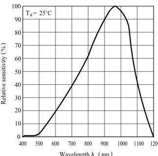
Fig. 2 Spectral Sensitivity
Power dissipation P
(mW
)
Ambient Temperature Ta (˚C)
Relative sensitivity
(%
)
Wavelength λ ( nm )
Fig. 3 Dark Current vs.
Fig. 4 Dark Current vs. Reverse Voltage
10- 6
10- 7
10- 8
10- 9
10- 10
10- 11
10- 12
Ambient temperature Ta (˚C)
Dark current I
d ( A ) 10-8 10-9 10-10 10-11 10-12 10-13
10- 3 10- 2 10- 1 10 102
Fig. 5 Terminal Capacitance vs.
Relative output (% )
Ambient Temperature
Ambient Temperature
Reverse Voltage
Dark current I
d
(
A
)
Reverse voltage VR (V)
Terminal capacitance C
t
(
pF
)
Reverse voltage VR (V) Ambient temperature Ta ( ˚C )
VR= 10V 5
Fig. 6 Relative Output vs. Ambient Temperature
Distance between infrared light emitting diode and photodiode shall be fixed when Isc= 25µA at IF= 20mA Ta= 25˚C
and Ta= 25˚C.
Ta= 25˚C Ta= 25˚C
1000 1100 1200
PD480PI/PD480PI1
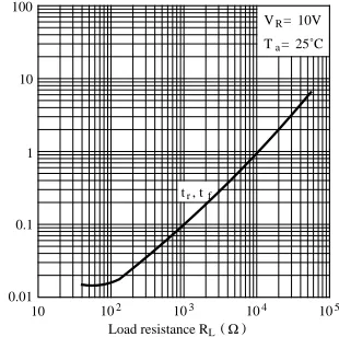
Test Circuit for Responce Time
0.01 1 10 Relative output (% ) 0.1 0.1 1 10 100
Angular displacement θ 0 100 20 40 60 80 100 tr tr Input Output Laser diode Pulse generator Output 10V + 90% 10% +20˚ +10˚ 0 + 90˚ + 80˚ + 70˚ + 50˚ + 60˚ + 40˚ + 30˚ - 30˚ - 40˚ - 50˚ - 60˚ - 70˚ - 80˚ - 90˚ GL480 PD480PI1 0.5 5 50
0.1 0.5 1 5 10 50 100
Fig. 7 Sensitivity Diagram
Fig. 8 Relative Output vs. Distance
10 102 103 104 105
Responce time t
r , t f ( µ s )
IF= 20mA Ta= 25˚C
VR= 10V Ta= 25˚C
IOUT=0.1mA
PD480PI/
RL
Relative radiant intensity
(%
)
- 10˚ - 20˚
tr, tf
Distance between emitter and detector d ( mm )
(T
a= 25˚C)
●
Please refer to the chapter “Precautions for Use.”
Fig. 9 Responce Time vs. Load Resistance
SPEC NO: KDA0438 REV NO: V.1 DATE: SEP/21/2001 PAGE: 1 OF 5
APPROVED: J.LU CHECKED: DRAWN: J.X.FU
L-53F3C L-53F3BT
L-53SF4C L-53SF4BT
L-53SF6C L-53SF6BT
L-53SF7C L-53SF7BT
T-1 3/4 (5mm) INFRA-RED EMITTING DIODE
Package Dimensions
Notes:
1. All dimensions are in millimeters (inches). 2. Tolerance is ±0.25(0.01") unless otherwise noted. 3. Lead spacing is measured where the lead emerge package. 4. Specifications are subject to change without notice.
Description
F3 Made with Gallium Arsenide Infrared Emitting diodes.
SF4 and SF6 and SF7 Made with Gallium Aluminum
Arsenide Infrared Emitting diodes.
Features
!MECHANICALLY AND SPECTRALLY MATCHED TO THE L-51P3C PHOTOTRANSISTOR.
SPEC NO: KDA0438 REV NO: V.1 DATE: SEP/21/2001 PAGE: 2 OF 5
APPROVED: J.LU CHECKED: DRAWN: J.X.FU
Electrical / Optical Characteristics at T
)=25
°°°°°
C
Selection Guide
Note:
1. θ1/2 is the angle from optical centerline where the luminous intensity is 1/2 the optical centerline value.
.
o
N
t
r
a
P
a
r
t
N
o
.
P
a
r
t
N
o
.
P
a
r
t
N
o
.
P
P
a
r
t
N
o
.
D e
D e
D
D e
D e
i
i
i
i
i
c
c
c
c
c
e
L
L
L
L
L
e
e
e
e
e
n
n
n
n
n
s
s
s
s
s
T
T
T
T
T
y
y
y
y
y
p
p
p
p
p
e
e
e
e
e
)
r
s
/
W
m
(
o
P
o
(
m
W
/
s
r
)
P
o
(
m
W
/
s
r
)
P
o
(
m
W
/
s
r
)
P
o
(
m
W
/
s
r
)
P
A
m
0
2
@
)
r
s
/
W
m
(
o
P
o
(
m
W
/
s
r
)
P
o
(
m
W
/
s
r
)
P
o
(
m
W
/
s
r
)
P
o
(
m
W
/
s
r
)
P
A
m
0
5
@
g
n
i
w
e
i
V
i
e
w
i
n
g
V
i
e
w
i
n
g
V
i
e
w
i
n
g
V
i
e
w
i
n
g
V
e
l
g
n
A
.
n
i
M .
i
n
M .
i
n
M .
i
n
M .
i
n
M
T
T
T
T
T
y
y
y
y
y
p
p
p
p
p
.
.
.
.
.
M .
M
M .
M .
M .
i
i
i
i
i
n
n
n
n
n
.
T
T
T
T
T
y
y
y
y
y
p
p
p
p
p
.
.
.
.
.
2 2
2 2
2 2
2
2 2
θ
θ
θ
θ
θ
1
1
1
1
1
/
/
/
/
/
2
C
3
F
3
5
-L
G
a
A
s
W
A
T
E
R
C
L
E
A
R
8
2
0
1
2
3
0
3
0
°
T
B
3
F
3
5
-L
G
a
A
s
B
L
U
E
T
R
A
N
S
.
5
2
0
8
3
0
3
0
°
C
4
F
S
3
5
-L
G
a
A
l
A
s
W
A
T
E
R
C
L
E
A
R
8
2
0
1
2
3
0
3
0
°
T
B
4
F
S
3
5
-L
G
a
A
l
A
s
B
L
U
E
T
R
A
N
S
.
5
2
0
8
3
0
3
0
°
C
6
F
S
3
5
-L
G
a
A
l
A
s
W
A
T
E
R
C
L
E
A
R
1
0
4
0
5
0
1
0
0
3
0
°
T
B
6
F
S
3
5
-L
G
a
A
l
A
s
B
L
U
E
T
R
A
N
S
.
1
0
4
0
5
0
1
0
0
3
0
°
C
7
F
S
3
5
-L
G
a
A
l
A
s
W
A
T
E
R
C
L
E
A
R
1
0
4
0
5
0
1
0
0
3
0
°
T
B
7
F
S
3
5
-L
G
a
A
l
A
s
B
L
U
E
T
R
A
N
S
.
1
0
4
0
5
0
1
0
0
3
0
°
m e t I mte I mte I mte
I mIte P NPP NP NP N/////N SSSSSyyyyymmmmmbbbbbooooolllll TTTTTyyyyyppppp... MMMMMaaaaaxxxxx... U tUU tU tU tnnnnniiiiit CCCCCooooonnnnndddddiiiiitttttiiiiiooooonnnnn
e g a t l o V d r a w r o F 3 F 4 F S 6 F S 7 F S VF 2 . 1 3 . 1 5 3 . 1 4 . 1 5 . 1 7 . 1 6 . 1 8 . 1
V IF=20mA
t n e r r u C e s r e v e R 3 F 4 F S 6 F S 7 F S
IR
-0 1 0 1 0 1 0 1 A
u VR=5V
e c n a t i c a p a C n o i t c n u J 3 F 4 F S 6 F S 7 F S C 0 9 0 9 0 3 0 3
- pF V=0 f=1MHz
h t g n e l e v a W l a r t c e p S k a e P 3 F 4 F S 6 F S 7 F S λP 0 4 9 0 8 8 0 6 8 0 5 8
- nm IF=20mA
h t d i w d n a B l a r t c e p S 3 F 4 F S 6 F S 7 F S λ ∆ 0 5 0 5 0 5 1 4
SPEC NO: KDA0438 REV NO: V.1 DATE: SEP/21/2001 PAGE: 3 OF 5
APPROVED: J.LU CHECKED: DRAWN: J.X.FU
Absolute Maximum Ratings at T
)=25
°°°°°
C
Notes:
1. 1/10 Duty Cycle, 0.1ms Pulse Width. 2. 4mm below package base.
m e t I mte I mte I mte I mte
I SSSSSyyyyymmmmmbbbbbooooolllll FFFFF33333&&&&&SSSSSFFFFF44444 SSSSSFFFFF66666&&&&&SSSSSFFFFF77777 UUUUUnnnnniiiiitttttsssss
n o i t a p i s s i D r e w o
P Pd 100 100 mW
t n e r r u C d r a w r o
F IF 50 50 mA
t n e r r u C d r a w r o F k a e
P IP 1.2 1 A
e g a t l o V e s r e v e
R VR 5 5 V
e r u t a r e p m e T g n i t a r e p
O Topr -40~+85 -40~+85 °C
e r u t a r e p m e T e g a r o t
S Tstg -40~+85 -40~+85 °C
SPEC NO: KDA0438 REV NO: V.1 DATE: SEP/21/2001 PAGE: 4 OF 5
APPROVED: J.LU CHECKED: DRAWN: J.X.FU
L-53SF4C, L-53SF4BT
SPEC NO: KDA0438 REV NO: V.1 DATE: SEP/21/2001 PAGE: 5 OF 5
APPROVED: J.LU CHECKED: DRAWN: J.X.FU
TL/H/5671
ADC0801/ADC0802/ADC0803/ADC0804/ADC0805
8-Bit
m
P
Compatible
A/D
Converters
December 1994
ADC0801/ADC0802/ADC0803/ADC0804/ADC0805
8-Bit
m
P Compatible A/D Converters
General Description
The ADC0801, ADC0802, ADC0803, ADC0804 and
ADC0805 are CMOS 8-bit successive approximation A/D converters that use a differential potentiometric ladderÐ similar to the 256R products. These converters are de-signed to allow operation with the NSC800 and INS8080A derivative control bus with TRI-STATEÉoutput latches di-rectly driving the data bus. These A/Ds appear like memory locations or I/O ports to the microprocessor and no inter-facing logic is needed.
Differential analog voltage inputs allow increasing the com-mon-mode rejection and offsetting the analog zero input voltage value. In addition, the voltage reference input can be adjusted to allow encoding any smaller analog voltage span to the full 8 bits of resolution.
Features
Y Compatible with 8080 mP derivativesÐno interfacing
logic needed - access time - 135 ns
Y Easy interface to all microprocessors, or operates
‘‘stand alone’’
Y Differential analog voltage inputs
Y Logic inputs and outputs meet both MOS and TTL volt-age level specifications
Y Works with 2.5V (LM336) voltage reference
Y On-chip clock generator
Y 0V to 5V analog input voltage range with single 5V
supply
Y No zero adjust required
Y 0.3×standard width 20-pin DIP package
Y 20-pin molded chip carrier or small outline package
Y Operates ratiometrically or with 5 VDC, 2.5 VDC, or ana-log span adjusted voltage reference
Key Specifications
Y Resolution 8 bits
Y Total error g(/4LSB,g(/2LSB andg1 LSB
Y Conversion time 100ms
Typical Applications
TL/H/5671 – 1
8080 Interface
TL/H/5671 – 31
Error Specification (Includes Full-Scale, Zero Error, and Non-Linearity)
Part Full- VREF/2e2.500 VDC VREF/2eNo Connection Number Scale (No Adjustments) (No Adjustments)
Adjusted
ADC0801 g(/4LSB
ADC0802 g(/2LSB
ADC0803 g(/2LSB
ADC0804 g1 LSB
ADC0805 g1 LSB
TRI-STATEÉis a registered trademark of National Semiconductor Corp. Z-80Éis a registered trademark of Zilog Corp.
Absolute Maximum Ratings
(Notes 1 & 2) If Military/Aerospace specified devices are required, please contact the National Semiconductor Sales Office/Distributors for availability and specifications.Supply Voltage (VCC) (Note 3) 6.5V
Voltage
Logic Control Inputs b0.3V toa18V
At Other Input and Outputs b0.3V to (VCCa0.3V)
Lead Temp. (Soldering, 10 seconds)
Dual-In-Line Package (plastic) 260§C
Dual-In-Line Package (ceramic) 300§C
Surface Mount Package
Vapor Phase (60 seconds) 215§C
Infrared (15 seconds) 220§C
Storage Temperature Range b65§C toa150§C
Package Dissipation at TAe25§C 875 mW
ESD Susceptibility (Note 10) 800V
Operating Ratings
(Notes 1 & 2)Temperature Range TMINsTAsTMAX
ADC0801/02LJ, ADC0802LJ/883 b55§CsTAsa125§C
ADC0801/02/03/04LCJ b40§CsTAsa85§C
ADC0801/02/03/05LCN b40§CsTAsa85§C
ADC0804LCN 0§CsT
Asa70§C
ADC0802/03/04LCV 0§CsTAsa70§C
ADC0802/03/04LCWM 0§CsTAsa70§C
Range of VCC 4.5 VDCto 6.3 VDC
Electrical Characteristics
The following specifications apply for VCCe5 VDC, TMINsTAsTMAXand fCLKe640 kHz unless otherwise specified.
Parameter Conditions Min Typ Max Units
ADC0801: Total Adjusted Error (Note 8) With Full-Scale Adj. g
(/4 LSB
(See Section 2.5.2)
ADC0802: Total Unadjusted Error (Note 8) VREF/2e2.500 VDC g(/2 LSB
ADC0803: Total Adjusted Error (Note 8) With Full-Scale Adj.
g(/2 LSB (See Section 2.5.2)
ADC0804: Total Unadjusted Error (Note 8) VREF/2e2.500 VDC g1 LSB
ADC0805: Total Unadjusted Error (Note 8) VREF/2-No Connection g1 LSB
VREF/2 Input Resistance (Pin 9) ADC0801/02/03/05 2.5 8.0 kX
ADC0804 (Note 9) 0.75 1.1 kX
Analog Input Voltage Range (Note 4) V(a) or V(b) Gnd – 0.05 VCCa0.05 VDC
DC Common-Mode Error Over Analog Input Voltage g(/16 g(/8 LSB
Range
Power Supply Sensitivity VCCe5 VDCg10% Over g(/16 g(/8 LSB
Allowed VIN(a) and VIN(b)
Voltage Range (Note 4)
AC Electrical Characteristics
The following specifications apply for VCCe5 VDCand TAe25§C unless otherwise specified.
Symbol Parameter Conditions Min Typ Max Units
TC Conversion Time fCLKe640 kHz (Note 6) 103 114 ms
TC Conversion Time (Note 5, 6) 66 73 1/fCLK
fCLK Clock Frequency VCCe5V, (Note 5) 100 640 1460 kHz
Clock Duty Cycle (Note 5) 40 60 %
CR Conversion Rate in Free-Running INTR tied to WR with 8770 9708 conv/s
Mode CSe0 VDC, fCLKe640 kHz
tW(WR)L Width of WR Input (Start Pulse Width) CSe0 VDC(Note 7) 100 ns
tACC Access Time (Delay from Falling CLe100 pF 135 200 ns
Edge of RD to Output Data Valid)
t1H, t0H TRI-STATE Control (Delay CLe10 pF, RLe10k 125 200 ns
from Rising Edge of RD to (See TRI-STATE Test
Hi-Z State) Circuits)
tWI, tRI Delay from Falling Edge 300 450 ns
of WR or RD to Reset of INTR
CIN Input Capacitance of Logic 5 7.5 pF
Control Inputs
COUT TRI-STATE Output 5 7.5 pF
Capacitance (Data Buffers)
CONTROL INPUTS[Note: CLK IN (Pin 4) is the input of a Schmitt trigger circuit and is therefore specified separately]
VIN(1) Logical ‘‘1’’ Input Voltage VCCe5.25 VDC 2.0 15 VDC
(Except Pin 4 CLK IN)
AC Electrical Characteristics
(Continued)The following specifications apply for VCCe5VDCand TMINsTAsTMAX, unless otherwise specified.
Symbol Parameter Conditions Min Typ Max Units
CONTROL INPUTS[Note: CLK IN (Pin 4) is the input of a Schmitt trigger circuit and is therefore specified separately]
VIN(0) Logical ‘‘0’’ Input Voltage VCCe4.75 VDC 0.8 VDC
(Except Pin 4 CLK IN)
IIN(1) Logical ‘‘1’’ Input Current VINe5 VDC 0.005 1 mADC
(All Inputs)
IIN(0) Logical ‘‘0’’ Input Current VINe0 VDC b1 b0.005 mADC
(All Inputs)
CLOCK IN AND CLOCK R
VTa CLK IN (Pin 4) Positive Going 2.7 3.1 3.5 VDC
Threshold Voltage
VTb CLK IN (Pin 4) Negative 1.5 1.8 2.1 VDC
Going Threshold Voltage
VH CLK IN (Pin 4) Hysteresis 0.6 1.3 2.0 VDC
(VTa)b(VTb)
VOUT(0) Logical ‘‘0’’ CLK R Output IOe360mA 0.4 VDC
Voltage VCCe4.75 VDC
VOUT(1) Logical ‘‘1’’ CLK R Output IOeb360mA 2.4 VDC
Voltage VCCe4.75 VDC
DATA OUTPUTS AND INTR
VOUT(0) Logical ‘‘0’’ Output Voltage
Data Outputs IOUTe1.6 mA, VCCe4.75 VDC 0.4 VDC
INTR Output IOUTe1.0 mA, VCCe4.75 VDC 0.4 VDC
VOUT(1) Logical ‘‘1’’ Output Voltage IOeb360mA, VCCe4.75 VDC 2.4 VDC
VOUT(1) Logical ‘‘1’’ Output Voltage IOeb10mA, VCCe4.75 VDC 4.5 VDC
IOUT TRI-STATE Disabled Output VOUTe0 VDC b3 mADC
Leakage (All Data Buffers) VOUTe5 VDC 3 mADC
ISOURCE VOUTShort to Gnd, TAe25§C 4.5 6 mADC
ISINK VOUTShort to VCC, TAe25§C 9.0 16 mADC
POWER SUPPLY
ICC Supply Current (Includes fCLKe640 kHz,
Ladder Current) VREF/2eNC, TAe25§C
and CSe5V
ADC0801/02/03/04LCJ/05 1.1 1.8 mA
ADC0804LCN/LCV/LCWM 1.9 2.5 mA
Note 1:Absolute Maximum Ratings indicate limits beyond which damage to the device may occur. DC and AC electrical specifications do not apply when operating the device beyond its specified operating conditions.
Note 2:All voltages are measured with respect to Gnd, unless otherwise specified. The separate A Gnd point should always be wired to the D Gnd.
Note 3:A zener diode exists, internally, from VCCto Gnd and has a typical breakdown voltage of 7 VDC.
Note 4:For VIN(b)tVIN(a) the digital output code will be 0000 0000. Two on-chip diodes are tied to each analog input (see block diagram) which will forward
conduct for analog input voltages one diode drop below ground or one diode drop greater than the VCCsupply. Be careful, during testing at low VCClevels (4.5V),
as high level analog inputs (5V) can cause this input diode to conduct–especially at elevated temperatures, and cause errors for analog inputs near full-scale. The spec allows 50 mV forward bias of either diode. This means that as long as the analog VINdoes not exceed the supply voltage by more than 50 mV, the output
code will be correct. To achieve an absolute 0 VDCto 5 VDCinput voltage range will therefore require a minimum supply voltage of 4.950 VDCover temperature variations, initial tolerance and loading.
Note 5:Accuracy is guaranteed at fCLKe640 kHz. At higher clock frequencies accuracy can degrade. For lower clock frequencies, the duty cycle limits can be extended so long as the minimum clock high time interval or minimum clock low time interval is no less than 275 ns.
Note 6:With an asynchronous start pulse, up to 8 clock periods may be required before the internal clock phases are proper to start the conversion process. The start request is internally latched, seeFigure 2 and section 2.0.
Note 7:The CS input is assumed to bracket the WR strobe input and therefore timing is dependent on the WR pulse width. An arbitrarily wide pulse width will hold the converter in a reset mode and the start of conversion is initiated by the low to high transition of the WR pulse (see timing diagrams).
Note 8:None of these A/Ds requires a zero adjust (see section 2.5.1). To obtain zero code at other analog input voltages see section 2.5 andFigure 5 .
Note 9:The VREF/2 pin is the center point of a two-resistor divider connected from VCCto ground. In all versions of the ADC0801, ADC0802, ADC0803, and ADC0805, and in the ADC0804LCJ, each resistor is typically 16 kX. In all versions of the ADC0804 except the ADC0804LCJ, each resistor is typically 2.2 kX.
Note 10:Human body model, 100 pF discharged through a 1.5 kXresistor.
Typical Performance Characteristics
Logic Input Threshold Voltage vs. Supply Voltage
Delay From Falling Edge of RD to Output Data Valid vs. Load Capacitance
CLK IN Schmitt Trip Levels vs. Supply Voltage
fCLKvs. Clock Capacitor
Full-Scale Error vs Conversion Time
Effect of Unadjusted Offset Error vs. VREF/2 Voltage
Output Current vs Temperature
Power Supply Current vs Temperature (Note 9)
Linearity Error at Low VREF/2 Voltages
TL/H/5671 – 2
TRI-STATE Test Circuits and Waveforms
t1H t1H, CLe10 pF
tre20 ns
t0H t0H, CLe10 pF
tre20 ns TL/H/5671 – 3
Timing Diagrams
(All timing is measured from the 50% voltage points)Output Enable and Reset INTR
Note: Read strobe must occur 8 clock periods (8/fCLK) after assertion of interrupt to guarantee reset of INTR. TL/H/5671 – 4
Typical Applications
(Continued)6800 Interface Ratiometric with Full-Scale Adjust
Note: before using caps at VINor VREF/2,
see section 2.3.2 Input Bypass Capacitors.
Absolute with a 2.500V Reference
*For low power, see also LM385-2.5
Absolute with a 5V Reference
Zero-Shift and Span Adjust: 2VsV
INs5V Span Adjust: 0VsVINs3V
TL/H/5671 – 5
Typical Applications
(Continued)Directly Converting a Low-Level Signal
VREF/2e256 mV
AmP Interfaced Comparator
For: VIN(a)lVIN(b)
OutputeFFHEX
For: VIN(a)kVIN(b) Outpute00HEX
1 mV Resolution withmP Controlled Range
VREF/2e128 mV
1 LSBe1 mV
VDACsVINs(VDACa256 mV)
Digitizing a Current Flow
TL/H/5671 – 6
Typical Applications
(Continued) Self-Clocking Multiple A/Ds*Use a large R value to reduce loading at CLK R output.
External Clocking
100 kHzsf
CLKs1460 kHz
Self-Clocking in Free-Running Mode
*After power-up, a momentary grounding of the WR input is needed to guarantee operation.
mP Interface for Free-Running A/D
Operating with ‘‘Automotive’’ Ratiometric Transducers
*VIN(b)e0.15 VCC
15% of VCCsVXDRs85% of VCC
Ratiometric with VREF/2 Forced
TL/H/5671 – 7
Typical Applications
(Continued)mP Compatible Differential-Input Comparator with Pre-Set VOS(with or without Hysteresis)
*SeeFigure 5 to select R value DB7e‘‘1’’ for VIN(a)lVIN(b)a(VREF/2)
Omit circuitry within the dotted area if hysteresis is not needed
Handlingg10V Analog Inputs
*Beckman InstrumentsÝ694-3-R10K resistor array
Low-Cost,mP Interfaced, Temperature-to-Digital Converter
mP Interfaced Temperature-to-Digital Converter
*Circuit values shown are for 0§CsT
Asa128§C
**Can calibrate each sensor to allow easy replacement, then A/D can be calibrated with a pre-set input voltage.
TL/H/5671 – 8
Typical Applications
(Continued) Handlingg5V Analog InputsTL/H/5671 – 33
*Beckman InstrumentsÝ694-3-R10K resistor array
Read-Only Interface
TL/H/5671 – 34
mP Interfaced Comparator with Hysteresis
TL/H/5671 – 35
Analog Self-Test for a System
TL/H/5671 – 36
Protecting the Input
TL/H/5671 – 9
A Low-Cost, 3-Decade Logarithmic Converter
TL/H/5671 – 37
*LM389 transistors
A, B, C, DeLM324A quad op amp Diodes are 1N914
Typical Applications
(Continued)3-Decade Logarithmic A/D Converter
Noise Filtering the Analog Input
fCe20 Hz
Uses Chebyshev implementation for steeper roll-off unity-gain, 2nd order, low-pass filter
Adding a separate filter for each channel increases system response time if an analog multiplexer is used
Multiplexing Differential Inputs
Output Buffers with A/D Data Enabled
*A/D output data is updated 1 CLK period prior to assertion of INTR
Increasing Bus Drive and/or Reducing Time on Bus
*Allows output data to set-up at falling edge of CS
TL/H/5671 – 10
Typical Applications
(Continued)Sampling an AC Input Signal
Note 1:Oversample whenever possible[keep fsl2f(b60)]to eliminate input frequency folding (aliasing) and to allow for the skirt response of the filter.
Note 2:Consider the amplitude errors which are introduced within the passband of the filter.
70% Power Savings by Clock Gating
(Complete shutdown takes&30 seconds.)
Power Savings by A/D and VREFShutdown
TL/H/5671 – 11
*Use ADC0801, 02, 03 or 05 for lowest power consumption. Note: Logic inputs can be driven to VCCwith A/D supply at zero volts.
Buffer prevents data bus from overdriving output of A/D when in shutdown mode.
Functional Description
1.0 UNDERSTANDING A/D ERROR SPECS
A perfect A/D transfer characteristic (staircase waveform) is shown inFigure 1a . The horizontal scale is analog input voltage and the particular points labeled are in steps of 1 LSB (19.53 mV with 2.5V tied to the VREF/2 pin). The digital output codes that correspond to these inputs are shown as Db1, D, and Da1. For the perfect A/D, not only will center-value (Ab1, A, Aa1, . . . . ) analog inputs produce the cor-rect output ditigal codes, but also each riser (the transitions between adjacent output codes) will be locatedg(/2LSB away from each center-value. As shown, the risers are ideal and have no width. Correct digital output codes will be pro-vided for a range of analog input voltages that extendg(/2
[image:36.612.90.506.170.641.2]LSB from the ideal center-values. Each tread (the range of analog input voltage that provides the same digital output code) is therefore 1 LSB wide.
Figure 1b shows a worst case error plot for the ADC0801. All center-valued inputs are guaranteed to produce the cor-rect output codes and the adjacent risers are guaranteed to be no closer to the center-value points thang(/4LSB. In
other words, if we apply an analog input equal to the center-valueg(/4LSB,we guarantee that the A/D will produce the correct digital code. The maximum range of the position of the code transition is indicated by the horizontal arrow and it is guaranteed to be no more than(/2LSB.
The error curve ofFigure 1c shows a worst case error plot for the ADC0802. Here we guarantee that if we apply an analog input equal to the LSB analog voltage center-value the A/D will produce the correct digital code.
Next to each transfer function is shown the corresponding error plot. Many people may be more familiar with error plots than transfer functions. The analog input voltage to the A/D is provided by either a linear ramp or by the discrete output steps of a high resolution DAC. Notice that the error is con-tinuously displayed and includes the quantization uncertain-ty of the A/D. For example the error at point 1 ofFigure 1a isa(/2LSB because the digital code appeared(/2LSB in advance of the center-value of the tread. The error plots always have a constant negative slope and the abrupt up-side steps are always 1 LSB in magnitude.
Transfer Function Error Plot
a) Accuracyeg0 LSB: A Perfect A/D
Transfer Function Error Plot
b) Accuracyeg(/4LSB
Transfer Function Error Plot
c) Accuracyeg(/2LSB TL/H/5671 – 12
FIGURE 1. Clarifying the Error Specs of an A/D Converter
Functional Description
(Continued) 2.0 FUNCTIONAL DESCRIPTIONThe ADC0801 series contains a circuit equivalent of the 256R network. Analog switches are sequenced by succes-sive approximation logic to match the analog difference in-put voltage[VIN(a)bVIN(b)]to a corresponding tap on the R network. The most significant bit is tested first and after 8 comparisons (64 clock cycles) a digital 8-bit binary code (1111 1111efull-scale) is transferred to an output latch and then an interrupt is asserted (INTR makes a high-to-low transition). A conversion in process can be interrupt-ed by issuing a second start command. The device may be operated in the free-running mode by connecting INTR to the WR input with CSe0. To ensure start-up under all pos-sible conditions, an external WR pulse is required during the first power-up cycle.
On the high-to-low transition of the WR input the internal SAR latches and the shift register stages are reset. As long as the CS input and WR input remain low, the A/D will re-main in a reset state.Conversion will start from 1 to 8 clock periods after at least one of these inputs makes a low-to-high transition .
A functional diagram of the A/D converter is shown in Fig-ure 2 . All of the package pinouts are shown and the major logic control paths are drawn in heavier weight lines. The converter is started by having CS and WR simulta-neously low. This sets the start flip-flop (F/F) and the result-ing ‘‘1’’ level resets the 8-bit shift register, resets the Inter-rupt (INTR) F/F and inputs a ‘‘1’’ to the D flop, F/F1, which is at the input end of the 8-bit shift register. Internal clock signals then transfer this ‘‘1’’ to the Q output of F/F1. The AND gate, G1, combines this ‘‘1’’ output with a clock signal to provide a reset signal to the start F/F. If the set signal is no longer present (either WR or CS is a ‘‘1’’) the start F/F is reset and the 8-bit shift register then can have the ‘‘1’’ clocked in, which starts the conversion process. If the set signal were to still be present, this reset pulse would have no effect (both outputs of the start F/F would momentarily be at a ‘‘1’’ level) and the 8-bit shift register would continue to be held in the reset mode. This logic therefore allows for wide CS and WR signals and the converter will start after at least one of these signals returns high and the internal clocks again provide a reset signal for the start F/F.
TL/H/5671 – 13
Note 1:CS shown twice for clarity.
Note 2:SAReSuccessive Approximation Register.
FIGURE 2. Block Diagram
[image:37.612.63.478.271.662.2]Functional Description
(Continued) After the ‘‘1’’ is clocked through the 8-bit shift register (which completes the SAR search) it appears as the input to the D-type latch, LATCH 1. As soon as this ‘‘1’’ is output from the shift register, the AND gate, G2, causes the new digital word to transfer to the TRI-STATE output latches. When LATCH 1 is subsequently enabled, the Q output makes a high-to-low transition which causes the INTR F/F to set. An inverting buffer then supplies the INTR input sig-nal.Note that this SET control of the INTR F/F remains low for 8 of the external clock periods (as the internal clocks run at
(/8of the frequency of the external clock). If the data output is continuously enabled (CS and RD both held low), the INTR output will still signal the end of conversion (by a high-to-low transition), because the SET input can control the Q output of the INTR F/F even though the RESET input is constantly at a ‘‘1’’ level in this operating mode. This INTR output will therefore stay low for the duration of the SET signal, which is 8 periods of the external clock frequency (assuming the A/D is not started during this interval). When operating in the free-running or continuous conver-sion mode (INTR pin tied to WR and CS wired lowÐsee also section 2.8), the START F/F is SET by the high-to-low transition of the INTR signal. This resets the SHIFT REGIS-TER which causes the input to the D-type latch, LATCH 1, to go low. As the latch enable input is still present, the Q output will go high, which then allows the INTR F/F to be RESET. This reduces the width of the resulting INTR output pulse to only a few propagation delays (approximately 300 ns).
When data is to be read, the combination of both CS and RD being low will cause the INTR F/F to be reset and the TRI-STATE output latches will be enabled to provide the 8-bit digital outputs.
2.1 Digital Control Inputs
The digital control inputs (CS, RD, and WR) meet standard T2L logic voltage levels. These signals have been renamed
when compared to the standard A/D Start and Output En-able labels. In addition, these inputs are active low to allow an easy interface to microprocessor control busses. For non-microprocessor based applications, the CS input (pin 1) can be grounded and the standard A/D Start function is obtained by an active low pulse applied at the WR input (pin 3) and the Output Enable function is caused by an active low pulse at the RD input (pin 2).
2.2 Analog Differential Voltage Inputs and Common-Mode Rejection
This A/D has additional applications flexibility due to the analog differential voltage input. The VIN(b) input (pin 7)
can be used to automatically subtract a fixed voltage value from the input reading (tare correction). This is also useful in 4 mA – 20 mA current loop conversion. In addition, common-mode noise can be reduced by use of the differential input. The time interval between sampling VIN(a) and VIN(b) is
4-(/2clock periods. The maximum error voltage due to this
slight time difference between the input voltage samples is given by:
DVe(MAX)e(VP) (2qfcm)
#
4.5 fCLK
J
,
where:
DVeis the error voltage due to sampling delay
VPis the peak value of the common-mode voltage
fcmis the common-mode frequency
As an example, to keep this error to(/4LSB (E5 mV) when operating with a 60 Hz common-mode frequency, fcm, and
using a 640 kHz A/D clock, fCLK, would allow a peak value of the common-mode voltage, VP, which is given by:
VPe
[DVe(MAX)(fCLK)]
(2qfcm) (4.5) or
VPe
(5c10b3) (640c103) (6.28) (60) (4.5) which gives
VPj1.9V.
The allowed range of analog input voltages usually places more severe restrictions on input common-mode noise lev-els.
An analog input voltage with a reduced span and a relatively large zero offset can be handled easily by making use of the differential input (see section 2.4 Reference Voltage).
2.3 Analog Inputs
2.3.1 Input Current
Normal Mode
Due to the internal switching action, displacement currents will flow at the analog inputs. This is due to on-chip stray capacitance to ground as shown inFigure 3 .
TL/H/5671 – 14
rONof SW 1 and SW 2j5 kX
rerONCSTRAYj5 kXc12 pFe60 ns
FIGURE 3. Analog Input Impedance
[image:38.612.83.509.167.664.2]Functional Description
(Continued) The voltage on this capacitance is switched and will result in currents entering the VIN(a) input pin and leaving the VIN(b) input which will depend on the analog differentialinput voltage levels. These current transients occur at the leading edge of the internal clocks. They rapidly decay and do not cause errors as the on-chip comparator is strobed at the end of the clock period.
Fault Mode
If the voltage source applied to the VIN(a) or VIN(b) pin
exceeds the allowed operating range of VCCa50 mV, large
input currents can flow through a parasitic diode to the VCC pin. If these currents can exceed the 1 mA max allowed spec, an external diode (1N914) should be added to bypass this current to the VCCpin (with the current bypassed with this diode, the voltage at the VIN(a) pin can exceed the VCCvoltage by the forward voltage of this diode).
2.3.2 Input Bypass Capacitors
Bypass capacitors at the inputs will average these charges and cause a DC current to flow through the output resist-ances of the analog signal sources. This charge pumping action is worse for continuous conversions with the VIN(a)
input voltage at full-scale. For continuous conversions with a 640 kHz clock frequency with the VIN(a) input at 5V, this
DC current is at a maximum of approximately 5mA. There-fore,bypass capacitors should not be used at the analog inputs or the VREF/2 pin for high resistance sources (l1 kX). If input bypass capacitors are necessary for noise filter-ing and high source resistance is desirable to minimize ca-pacitor size, the detrimental effects of the voltage drop across this input resistance, which is due to the average value of the input current, can be eliminated with a full-scale adjustment while the given source resistor and input bypass capacitor are both in place. This is possible because the average value of the input current is a precise linear func-tion of the differential input voltage.
2.3.3 Input Source Resistance
Large values of source resistance where an input bypass capacitor is not used,will not cause errors as the input cur-rents settle out prior to the comparison time. If a low pass filter is required in the system, use a low valued series resis-tor (s1 kX) for a passive RC section or add an op amp RC
active low pass filter. For low source resistance applica-tions, (s1 kX), a 0.1mF bypass capacitor at the inputs will
prevent noise pickup due to series lead inductance of a long wire. A 100Xseries resistor can be used to isolate this ca-pacitorÐboth the R and C are placed outside the feedback loopÐfrom the output of an op amp, if used.
2.3.4 Noise
The leads to the analog inputs (pin 6 and 7) should be kept as short as possible to minimize input noise coupling. Both noise and undesired digital clock coupling to these inputs can cause system errors. The source resistance for these inputs should, in general, be kept below 5 kX. Larger values of source resistance can cause undesired system noise pickup. Input bypass capacitors, placed from the analog in-puts to ground, will eliminate system noise pickup but can create analog scale errors as these capacitors will average the transient input switching currents of the A/D (see sec-tion 2.3.1.). This scale error depends on both a large source
resistance and the use of an input bypass capacitor. This error can be eliminated by doing a full-scale adjustment of the A/D (adjust VREF/2 for a proper full-scale readingÐsee
section 2.5.2 on Full-Scale Adjustment) with the source re-sistance and input bypass capacitor in place.
2.4 Reference Voltage
2.4.1 Span Adjust
For maximum applications flexibility, these A/Ds have been designed to accommodate a 5 VDC, 2.5 VDCor an adjusted
voltage reference. This has been achieved in the design of the IC as shown inFigure 4 .
TL/H/5671 – 15
FIGURE 4. The VREFERENCEDesign on the IC Notice that the reference voltage for the IC is either(/2of the voltage applied to the VCCsupply pin, or is equal to the
voltage that is externally forced at the VREF/2 pin. This
al-lows for a ratiometric voltage reference using the VCC sup-ply, a 5 VDCreference voltage can be used for the VCC
supply or a voltage less than 2.5 VDCcan be applied to the
VREF/2 input for increased application flexibility. The inter-nal gain to the VREF/2 input is 2, making the full-scale differ-ential input voltage twice the voltage at pin 9.
An example of the use of an adjusted reference voltage is to accommodate a reduced spanÐor dynamic voltage range of the analog input voltage. If the analog input voltage were to range from 0.5 VDCto 3.5 VDC, instead of 0V to 5 VDC,
the span would be 3V as shown inFigure 5 . With 0.5 VDC
applied to the VIN(b) pin to absorb the offset, the reference
voltage can be made equal to(/2of the 3V span or 1.5 VDC.
The A/D now will encode the VIN(a) signal from 0.5V to 3.5 V with the 0.5V input corresponding to zero and the 3.5 VDC input corresponding to full-scale. The full 8 bits of resolution are therefore applied over this reduced analog input voltage range.
[image:39.612.289.476.209.419.2]Functional Description
(Continued)*Add if VREF/2s1 VDCwith LM358
to draw 3 mA to ground.
TL/H/5671 – 16
a) Analog Input Signal Example b) Accommodating an Analog Input from 0.5V (Digital Oute e00HEX) to 3.5V
(Digital OuteFFHEX)
FIGURE 5. Adapting the A/D Analog Input Voltages to Match an Arbitrary Input Signal Range
2.4.2 Reference Accuracy Requirements
The converter can be operated in a ratiometric mode or an absolute mode. In ratiometric converter applications, the magnitude of the reference voltage is a factor in both the output of the source transducer and the output of the A/D converter and therefore cancels out in the final digital output code. The ADC0805 is specified particularly for use in ratio-metric applications with no adjustments required. In abso-lute conversion applications, both the initial value and the temperature stability of the reference voltage are important factors in the accuracy of the A/D converter. For VREF/2 voltages of 2.4 VDCnominal value, initial errors of g10 mVDCwill cause conversion errors ofg1 LSB due to the
gain of 2 of the VREF/2 input. In reduced span applications, the initial value and the stability of the VREF/2 input voltage
become even more important. For example, if the span is reduced to 2.5V, the analog input LSB voltage value is cor-respondingly reduced from 20 mV (5V span) to 10 mV and 1 LSB at the VREF/2 input becomes 5 mV. As can be seen,
this reduces the allowed initial tolerance of the reference voltage and requires correspondingly less absolute change with temperature variations. Note that spans smaller than 2.5V place even tighter requirements on the initial accuracy and stability of the reference source.
In general, the magnitude of the reference voltage will re-quire an initial adjustment. Errors due to an improper value of reference voltage appear as full-scale errors in the A/D transfer function. IC voltage regulators may be used for ref-erences if the ambient temperature changes are not exces-sive. The LM336B 2.5V IC reference diode (from National Semiconductor) has a temperature stability of 1.8 mV typ (6 mV max) over 0§CsTAsa70§C. Other temperature range parts are also available.
2.5 Errors and Reference Voltage Adjustments
2.5.1 Zero Error
The zero of the A/D does not require adjustment. If the minimum analog input voltage value, VIN(MIN), is not ground,
a zero offset can be done. The converter can be made to output 0000 0000 digital code for this minimum input voltage by biasing the A/D VIN(b) input at this VIN(MIN)value (see
Applications section). This utilizes the differential mode op-eration of the A/D.
The zero error of the A/D converter relates to the location of the first riser of the transfer function and can be mea-sured by grounding the VIN(b) input and applying a small
magnitude positive voltage to the VIN(a) input. Zero error is the difference between the actual DC input voltage that is necessary to just cause an output digital code transition from 0000 0000 to 0000 0001 and the ideal(/2LSB value ((/2LSBe9.8 mV for VREF/2e2.500 VDC).
2.5.2 Full-Scale
The full-scale adjustment can be made by applying a differ-ential input voltage that is 1(/2LSB less than the desired analog full-scale voltage range and then adjusting the mag-nitude of the VREF/2 input (pin 9 or the VCCsupply if pin 9 is not used) for a digital output code that is just changing from 1111 1110 to 1111 1111.
[image:40.612.88.506.72.327.2]Functional Description
(Continued) 2.5.3 Adjusting for an Arbitrary Analog Input VoltageRange
If the analog zero voltage of the A/D is shifted away from ground (for example, to accommodate an analog input sig-nal that does not go to ground) this new zero reference should be properly adjusted first. A VIN(a) voltage that
equals this desired zero reference plus(/2LSB (where the LSB is calculated for the desired analog span, 1 LSBe ana-log span/256) is applied to pin 6 and the zero reference voltage at pin 7 should then be adjusted to just obtain the 00HEXto 01HEXcode transition.
The full-scale adjustment should then be made (with the proper VIN(b) voltage applied) by forcing a voltage to the
VIN(a) input which is given by: VIN(a) fs adjeVMAXb1.5
Ð
(VMAXbVMIN)
256
(
,where:
VMAXeThe high end of the analog input range
and
VMINethe low end (the offset zero) of the analog range. (Both are ground referenced.)
The VREF/2 (or VCC) voltage is then adjusted to provide a
code change from FEHEXto FFHEX. This completes the
ad-justment procedure.
2.6 Clocking Option
The clock for the A/D can be derived from the CPU clock or an external RC can be added to provide self-clocking. The CLK IN (pin 4) makes use of a Schmitt trigger as shown in Figure 6 .
fCLKj
1 1.1 RC Rj10 kX
TL/H/5671 – 17
FIGURE 6. Self-Clocking the A/D
Heavy capacitive or DC loading of the clock R pin should be avoided as this will disturb normal converter operation. Loads less than 50 pF, such as driving up to 7 A/D convert-er clock inputs from a single clock R pin of 1 convconvert-ertconvert-er, are allowed. For larger clock line loading, a CMOS or low power TTL buffer or PNP input logic should be used to minimize the loading on the clock R pin (do not use a standard TTL buffer).
2.7 Restart During a Conversion
If the A/D is restarted (CS and WR go low and return high) during a conversion, the converter is reset and a new con-version is started. The output data latch is not updated if the
conversion in process is not allowed to be completed, there-fore the data of the previous conversion remains in this latch. The INTR output simply remains at the ‘‘1’’ level.
2.8 Continuous Conversions
For operation in the free-running mode an initializing pulse should be used, following power-up, to ensure circuit opera-tion. In this application, the CS input is grounded and the WR input is tied to the INTR output. This WR and INTR node should be momentarily forced to logic low following a power-up cycle to guarantee operation.
2.9 Driving the Data Bus
This MOS A/D, like MOS microprocessors and memories, will require a bus driver when the total capacitance of the data bus gets large. Other circuitry, which is tied to the data bus, will add to the total capacitive loading, even in TRI-STATE (high impedance mode). Backplane bussing also greatly adds to the stray capacitance of the data bus. There are some alternatives available to the designer to handle this problem. Basically, the capacitive loading of the data bus slows down the response time, even though DC specifications are still met. For systems operating with a relatively slow CPU clock frequency, more time is available in which to establish proper logic levels on the bus and therefore higher capacitive loads can be driven (see typical characteristics curves).
At higher CPU clock frequencies time can be extended for I/O reads (and/or writes) by inserting wait states (8080) or using clock extending circuits (6800).
Finally, if time is short and capacitive loading is high, exter-nal bus drivers must be used. These can be TRI-STATE buffers (low power Schottky such as the DM74LS240 series is recommended) or special higher drive current products which are designed as bus drivers. High current bipolar bus drivers with PNP inputs are recommended.
2.10 Power Supplies
Noise spikes on the VCCsupply line can cause conversion errors as the comparator will respond to this noise. A low inductance tantalum filter capacitor should be used close to the converter VCCpin and values of 1mF or greater are recommended. If an unregulated voltage is available in the system, a separate LM340LAZ-5.0, TO-92, 5V voltage regu-lator for the converter (and other analog circuitry) will greatly reduce digital noise on the VCCsupply.
2.11 Wiring and Hook-Up Precautions
Standard digital wire wrap sockets are not satisfactory for breadboarding this A/D converter. Sockets on PC boards can be used and all logic signal wires and leads should be grouped and kept as far away as possible from the analog signal leads. Exposed leads to the analog inputs can cause undesired digital noise and hum pickup, therefore shielded leads may be necessary in many applications.
[image:41.612.63.260.88.525.2]Functional Description
(Continued) A single point analog ground that is separate from the logic ground points should be used. The power supply bypass capacitor and the self-clocking capacitor (if used) should both be returned to digital ground. Any VREF/2 bypassca-pacitors, analog input filter caca-pacitors, or input signal shield-ing should be returned to the analog ground point. A test for proper grounding is to measure the zero error of the A/D converter. Zero errors in excess of(/4LSB can usually be traced to improper board layout and wiring (see section 2.5.1 for measuring the zero error).
3.0 TESTING THE A/D CONVERTER
There are many degrees of complexity associated with test-ing an A/D converter. One of the simplest tests is to apply a known analog input voltage to the converter and use LEDs to display the resulting digital output code as shown in Fig-ure 7 .
For ease of testing, the VREF/2 (pin 9) should be supplied
with 2.560 VDC and a VCC supply voltage of 5.12 VDC should be used. This provides an LSB value of 20 mV. If a full-scale adjustment is to be made, an analog input voltage of 5.090 VDC(5.120 – 1(/2LSB) should be applied to the VIN(a) pin with the VIN(b) pin grounded. The value of
the VREF/2 input voltage should then be adjusted until the
digital output code is just changing from 1111 1110 to 1111 1111. This value of VREF/2 should then be used for all the tests.
The digital output LED display can be decoded by dividing the 8 bits into 2 hex characters, the 4 most significant (MS) and the 4 least significant (LS). Table I shows the fractional binary equivalent of these two 4-bit groups. By adding the voltages obtained from the ‘‘VMS’’ and ‘‘VLS’’ columns in Table I, the nominal value of the digital display (when
TL/H/5671 – 18
FIGURE 7. Basic A/D Tester
VREF/2e2.560V) can be determined. For example, for an
output LED display of 1011 0110 or B6 (in hex), the voltage values from the table are 3.520a 0.120 or 3.640 VDC.
These voltage values represent the center-values of a per-fect A/D converter. The efper-fects of quantization error have to be accounted for in the interpretation of the test results. For a higher speed test system, or to obtain plotted data, a digital-to-analog converter is needed for the test set-up. An accurate 10-bit DAC can serve as the precision voltage source for the A/D. Errors of the A/D under test can be expressed as either analog voltages or differences in 2 digi-tal words.
A basic A/D tester that uses a DAC and provides the error as an analog output voltage is shown inFigure 8 . The 2 op amps can be eliminated if a lab DVM with a numerical sub-traction feature is available to read the difference voltage, ‘‘A – C’’, directly. The analog input voltage can be supplied by a low frequency ramp generator and an X-Y plotter can be used to provide analog error (Y axis) versus analog input (X axis).
For operation with a microprocessor or a computer-based test system, it is more convenient to present the errors digi-tally. This can be done with the circuit ofFigure 9 , where the output code transitions can be detected as the 10-bit DAC is incremented. This provides(/4LSB steps for the 8-bit A/D under test. If the results of this test are automatically plotted with the analog input on the X axis and the error (in LSB’s) as the Y axis, a useful transfer function of the A/D under test results. For acceptance testing, the plot is not neces-sary and the testing speed can be increased by establishing internal limits on the allowed error for each code.
4.0 MICROPROCESSOR INTERFACING
To dicuss the interface with 8080A and 6800 microproces-sors, a common sample subroutine structure is used. The microprocessor starts the A/D, reads and stores the results of 16 successive conversions, then returns to the user’s program. The 16 data bytes are stored in 16 successive memory locations. All Data and Addresses will be given in hexadecimal form. Software and hardware details are pro-vided separately for each type of microprocessor.
4.1 Interfacing 8080 Microprocessor Derivatives (8048, 8085)
This converter has been designed to directly interface with derivatives of the 8080 microprocessor. The A/D can be mapped into memory space (using standard memory ad-dress decoding for CS and the MEMR and MEMW strobes) or it can be controlled as an I/O device by using the I/O R and I/O W strobes and decoding the address bits A0
x
A7 (or address bits A8x
A15 as they will contain the same 8-bit address information) to obtain the CS input. Us-ing the I/O space provides 256 additional addresses and may allow a simpler 8-bit address decoder but the data can only be input to the accumulator. To make use of the addi-tional memory reference instructions, the A/D should be m