V. Jagannathan
Devices and Circuits
Power
Electronics
Power
V. Jagannathan
Professor and HeadDepartment of Electrical and Electronics Engineering Coimbatore Institute of Technology
Coimbatore
SECOND EDITION
New Delhi-110001
2011
Power Electronics
V. Jagannathan
© 2011 by PHI Learning Private Limited, New Delhi. All rights reserved. No part of this book may be reproduced in any form, by mimeograph or any other means, without permission in writing from the publisher.
ISBN-978-81-203-4196-8
The export rights of this book are vested solely with the publisher.
Seventh Printing (Second Edition) L L November, 2010
iii
Contents
Preface xi
1. Introduction
1–19
1.1 What is Power Electronics? 1
1.2 History 1
1.3 Power Electronics Applications 2
1.4 Power Semiconductor Devices and Their Classifications 3
1.5 Power Semiconductor Devices: Characteristics and Ratings 5
1.6 Ideal and Real Switches: Comparison of Characteristics 7
1.6.1 Ideal Switch Characteristics 7
1.6.2 Desirable Characteristics of a Real Switch 7
1.6.3 Power Loss Characteristics of an Ideal Switch 7
1.6.4 Power Loss Characteristics in a Real Switch 8
1.7 Power Electronic Systems 10
1.8 Types of Power Electronic Circuits/Converters 11
1.9 Merits and Demerits of Power Electronic Converters 12
1.10 Recent Developments 12
Summary 13
Solved Examples 14
Review Questions 18
Problems 18
2. Power Switching Devices and their Characteristics
20–108
2.1 Preliminaries 20
2.2 Power Diodes 20
2.2.1 Diode V–I Characteristics 21
2.2.2 Diode Reverse Recovery Characteristics 22
2.2.3 Types and Ratings of Power Diodes 22
2.3 Thyristors 24
2.3.1 Structure, Symbol, and V–I Characteristics 24
2.3.2 Transistor Analogy 26
2.3.3 Thyristor Turn-on Methods 27
2.3.4 Thyristor Turn-off Methods 30
2.4 Switching Characteristics of Thyristors 30
2.4.1 Switching Characteristics during Turn-on 30
2.4.2 Switching Characteristics during Turn-off 32
2.5 Thyristor Gate Characteristics 33
2.6 Thyristor Commutation Methods 35
2.6.1 Natural Commutation 35
2.6.2 Forced Commutation 35
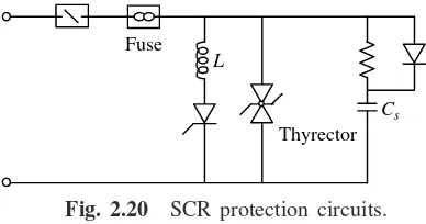
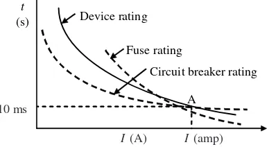
2.7 Thyristor Protection 39
2.7.1 Over Voltage Protection 40
2.7.2 Suppression of Overvoltages 40
2.7.3 Overcurrent Protection 41
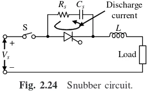
2.7.4 Snubber Circuits 44
2.8 Thyristor Ratings 44
2.8.1 Anode Voltage Ratings 45
2.8.2 Current Ratings 46
2.8.3 Surge Current Rating 49
2.8.4 I2t Rating 49
2.8.5 di/dt Rating 50
2.9 Series and Parallel Operation of Thyristors 50
2.9.1 Series Operation 51
2.9.2 Parallel Operation 53
2.10 Triggering of Thyristors 55
2.10.1 Triggering of Thyristors in Series 55
2.10.2 Triggering of Parallel Connected SCRs 57
2.11 Heat Sinks, Heating, Cooling and Mounting of Thyristors 57
2.11.1 Thermal Resistance 58
2.11.2 Thyristor Heat Sinks 59
2.12 Thyristor Trigger Circuits 59
2.12.1 RC Firing Circuits 59
2.12.2 Synchronized UJT Triggering (or Ramp Triggering) 61
2.12.3 Ramp and Pedestal Triggering 62
2.12.4 Pulse Transformers 63
2.13 Other Thyristor Devices 64
2.13.1 TRIAC 64
2.13.2 DIAC 65
2.13.3 LASCR 66
2.13.4 Programmable Unijunction Transistor (PUT) 67
2.13.5 Silicon Unilateral Switch (SUS) 67
2.13.6 Reverse Conducting Thyristor (RCT) 67
2.14 Power Transistors 73
2.14.1 Bipolar Junction Transistor (BJT) 73
2.15 Power MOSFET 78
2.16 Comparison of MOSFET and BJT 82
2.17 Insulated Gate Bipolar Transistor (IGBT) 82
2.17.1 Basic Structure 83
2.17.2 Equivalent Circuit 84
2.17.3 Operation Models 85
2.17.4 Output Characteristics 85
2.17.5 Transfer Characteristics 86
2.17.6 Switching Characteristics 86
2.17.7 Latch-up 87
2.17.8 Safe Operating Area (SOA) 87
2.17.9 Applications 87
2.18 MOS Controlled Thyristor (MCT) 88
2.19 Typical Rating of High Power Devices 88
2.20 Driver Circuits for Gate Commutation Devices 89
2.20.1 GATE Drive Circuits for Power MOSFET 89
2.20.2 Driver Circuits for MOSFET 90
2.20.3 Driver Circuits for IGBT 91
2.20.4 Base-Drive Circuits for Power BJT 92
2.20.5 GATE Drive Circuits for GTO 92
Solved Examples 93
Review Questions 104
Problems 108
3. AC to DC Converters
109–166
3.1 Preliminaries 109
3.2 The Principle of Phase Control 110
3.3 Converter Classifications 113
3.3.1 Single-phase Half Wave Thyristor Rectifier with RL Load 114
3.3.2 Single-phase Half Wave Thyristor Rectifier with RL Load and
Free-wheeling Diode 116
3.3.3 Single-phase Half Wave Thyristor Rectifier with RLE Load 117
3.4 Single-phase Full Wave Thyristor Converters 118
3.4.1 Single-phase Full Wave Mid-point Thyristor Converter 118
3.5 Single-phase Full Wave Bridge Converters 120
3.5.1 Single-phase Bridge Rectifier Connected to Resistance Load 120
3.5.2 Series RL Load 121
3.5.3 RL Load with Free-wheeling Diode 122
3.6 Full Wave Bridge Rectifier Feeding RLE Load 122
3.7 Single-phase Semi-converter 124
3.8 Calculation of Active and Reactive Power Inputs 125
3.9 Effect of Load Inductance 127
3.10 Three-phase Thyristor Converter Circuits 127
3.10.2 Three-phase Full Converters 129
3.10.3 Line Commutated Three-phase Inverter 133
3.10.4 Three-phase Semi-converters 134
3.11 Effect of Source Impedance on the Performance of Converters 135
3.11.1 Single-phase Full Converter 136
3.11.2 Three-phase Full Converter Bridge 138
3.12 Dual Converters 139
3.12.1 Dual Converter without Circulating Current 141
3.12.2 Dual Converter with Circulating Current 141
3.13 Single Phase Series Converters 142
3.13.1 Two Semiconverters in Series 142
3.13.2 Two Single Phase Full Converters in Series 144
3.13.3 Twelve-pulse Converters 146
3.14 Gating Circuits 147
3.15 Cosine Firing Scheme 147
Solved Examples 149
Review Questions 161
Problems 164
4. AC to AC Converters
167–196
4.1 Preliminaries 167
4.2 AC Voltage Controllers 167
4.2.1 Types of AC Voltage Controllers 168
4.3 Methods of Voltage Control 170
4.3.1 Single-phase AC Voltage Controller Supplying R Loads
(Phase Control) 170
4.3.2 Single-phase AC Voltage Controller Supplying R Loads
(Integral Cycle Control) 172
4.4 Single-phase Voltage Controller Supplying RL Loads 173
4.5 Three-phase AC Voltage Controller 176
4.6 Single-phase Transformer Tap Changer 178
4.7 Cycloconverters 180
4.7.1 Principle of Operation 181
4.7.2 Single-phase to Single-phase Cycloconverter Feeding RL Load 183
4.7.3 Three-phase to Single-phase Cycloconverters 184
4.7.4 Three-phase to Three-phase Cycloconverter 187
4.8 Output Voltage Equation 188
4.9 Effect of Source Inductance 189
Solved Examples 190
Review Questions 194
Problems 195
5. DC to DC Converters (Choppers)
197–248
5.1 Preliminaries 197
5.3 Control Schemes 199
5.3.1 Constant Frequency Scheme 199
5.3.2 Variable Frequency Scheme 199
5.3.3 Current Limit Control (CLC) 200
5.4 Step Up Choppers 200
5.5 Chopper Circuits: Classification 202
5.6 Steady State Time–Domain Analysis of Type A Chopper 206
5.7 Thyristor Based Chopper Circuits 208
5.7.1 Voltage Commutated Chopper 209
5.7.2 Current Commutated Chopper 212
5.7.3 Load Commutated Chopper 214
5.8 Multiphase Choppers 215
5.9 Switch Mode Power Supplies (SMPS) 217
5.10 Switch Mode DC–DC Converter (without Isolation) 218
5.10.1 Buck Converter 218
5.10.2 Boost-type Converter 220
5.10.3 Buck Boost Converter 223
5.10.4 Cuk Converters 225
5.11 Switch Mode DC–DC Converter (with Isolation) 225
5.11.1 Fly Back Converter 226
5.11.2 Push–Pull Converter 227
5.11.3 Half-bridge Converter 228
5.11.4 Full-bridge Converter 229
5.12 Resonant Converters 230
5.12.1 Zero-current Switching Resonant Converters 231
5.12.2 Zero-voltage Switching Resonant Converters 236
5.12.3 Comparison between ZCS and ZVS converters 240
Solved Examples 241
Review Questions 246
Problems 247
6. Inverters
249–298
6.1 Preliminaries 249
6.2 Classification 249
6.3 Parallel Inverters 250
6.3.1 Basic Parallel Inverter 250
6.3.2 Modified Parallel Inverter 252
6.4 Series Inverters 253
6.4.1 Basic Series Inverter 253
6.4.2 Modifications of Series Inverter 255
6.5 Single-phase Bridge Voltage Source Inverter 256
6.5.1 Single-phase Half Bridge Inverter 256
6.5.2 Single-phase Full Bridge Inverter 259
6.6 Force Commutated Thyristor Inverter 261
6.6.1 McMurray Inverter (Auxiliary Commutated Inverter) 261
6.6.2 Modified McMurray Full Bridge Inverter 263
6.6.3 McMurray–Bedford Half Bridge Inverter (Complementary Impulse
Commutated Inverter) 264
6.7 Three-phase Bridge Inverters 267
6.7.1 Three-phase Inverter under 180° Mode Operation 268
6.7.2 Three-phase Inverter under 120° Mode Operation 271
6.8 Voltage Control in Single-phase Inverters 274
6.8.1 External Control of the AC Output Voltage 274
6.8.2 External Control of the DC Input Voltage Through Variable DC Link 275
6.8.3 Internal Control of the Inverter Voltage 276
6.8.4 Pulse Width Modulated Inverters 277
6.9 Voltage Control of Three-phase Inverter 281
6.10 Harmonic Reduction in the Output Voltage 282
6.10.1 Harmonic Reduction by Transformer Connections 282
6.10.2 Harmonic Reduction by Multiple Commutation in Each Half Cycle 284
6.11 Current Source Inverter 286
6.11.1 Single-phase Capacitor Commutated Current Source Inverter
with R Load 286
6.11.2 Single-phase Auto-sequential Commutated Inverter (One-phase ASCI) 287
6.12 Three-phase Current Source Inverter 288
Solved Examples 289
Review Questions 296
Problems 298
7. Power Controllers: Their Applications
299–334
7.1 Preliminaries 299
7.2 DC Motor Speed Control 299
7.2.1 Principle of Speed Control 300
7.3 Phase Controlled Converters 301
7.3.1 Single-phase DC Drives 303
7.3.2 Three-phase DC Drives 308
7.3.3 Dual Converter Drives 311
7.4 Chopper Controlled DC Drives 312
7.5 AC Drives 315
7.5.1 Induction Motor Drives 315
7.5.2 Speed Control by Stator Voltage Control 316
7.5.3 Variable Voltage Variable Frequency Control 317
7.5.4 Speed Control by Chopper Controlled Rotor Resistance 318
7.5.5 Slip Power Recovery Control 319
7.6 Synchronous Motor Control 320
7.7 Static Circuit Breakers 320
7.7.1 DC Circuit Breakers 321
7.8 HVDC Transmission 322
7.8.1 Types of HVDC Lines 323
7.8.2 Converter Station 324
7.9 Static Var Systems 325
7.9.1 Thyristor Controlled Reactor-fixed (TCR) Capacitor 326
7.9.2 Thyristor Switched Capacitor–Thyristor Controlled Reactor (TSC–TCR) 326
7.10 Uninterrupted Power Supply (UPS) 327
7.10.1 On-Line UPS 327
7.10.2 Off-Line UPS 329
7.10.3 Salient Features of an On-Line Inverter 330
7.10.4 Inverters 331
7.10.5 Transfer Switch 331
Solved Examples 332
Review Questions 334
8. Microcontroller Based Control and Protection Circuits
335–364
8.1 Preliminaries 335
8.2 The 8051 Microcontroller 336
8.2.1 The 8051 Pin Configuration 337
8.2.2 8051 Architecture 339
8.2.3 Memory Organization 339
8.2.4 The Special Function Register 340
8.2.5 Timers/Counters 341
8.2.6 The Serial Interface 341
8.2.7 The Interrupts 341
8.2.8 The Power Control Register (PCON) 342
8.3 The Instruction Set 342
8.3.1 Addressing Modes 342
8.3.2 Arithmetic Instructions 343
8.3.3 Logical Instructions 343
8.3.4 Data Transfer Instructions 344
8.3.5 Boolean Instructions 345
8.3.6 The Program Branching and Machine Control Instructions 345
8.3.7 Instruction Timing 346
8.4 Interfacing the 8051 Microcontroller 346
8.4.1 Interfacing External Memory 346
8.4.2 Interfacing an Input/Output Device 347
8.4.3 Interfacing an Analog to Digital Converter 348
8.4.4 Interfacing a Digital to Analog Converter 349
8.4.5 Interfacing a Relay and an Optocoupler 349
8.4.6 Interfacing a Pulse Transformer 351
8.5 Applications 352
8.5.1 SCR Triggering 352
8.5.2 Cycloconverter 354
8.5.3 Fault Diagnosis in Three-phase Thyristor Converters Using
8.6 ASICs for Motor Control Applications 360
8.6.1 Need for DSP Based Motor Control 360
8.6.2 Motor Control Peripherals 361
Review Questions 364
References
365
xi
Preface
Rapid developments in power electronics during the last few decades have revolutionized the art of power modulation and control. Today, power semiconductor devices and converters using these devices can handle high voltages and currents at high speeds. Their applications in different areas are ever increasing aided by the use of sophisticated digital systems like microcontrollers and computers. It is felt that this ever-growing subject, power electronics, must be learnt by students with clarity and ease. It is therefore written in a simple straightforward style emphasizing the core concepts underlying various power electronics circuits without delving deep into complex, circuitous and mathematical elaborations. This book is expected to serve as a student-friendly text to the undergraduate students of electrical and electronics engineering. It can also be used as a textbook for one-semester course in power electronics.
The Book
The text begins with an introductory chapter on the area of power electronics with discussions ranging around the characteristics and ratings of power semiconductor devices. Further, the chapter gives a bird’s eye view of various types of converter circuits along with their major applications. Chapter 2 details the underlying principle of operation of practical power semiconductor devices such as power diodes, thyristors and devices like DIAC, TRIAC and LASCR belonging to thyristor family. An elaborate treatment of gate-commutated devices like GTOpower BJT, power MOSFET, and IGBT is also presented in the chapter 2. Chapters 3, 4 and 5 unlock the operating principles of various types of converters, — ac to dc converters, ac to ac converters and dc to dc converters (choppers and SMPS). These chapters integrate within themselves different methods of phase, frequency and voltage control for achieving high level of performance. Analysis of each class of converter circuit is undertaken leading to the evaluation of their performance parameters.
protection circuits have enhanced the quality of power modulation and control. This chapter not only gives an overview of various microcontroller chips but also considers their applications in triggering and fault diagnosis.
Each chapter is accompanied by adequate number of solved problems, review questions and problems involving both short and lengthy answers and solutions. The solved problems are so chosen that going through them reinforces the understanding of the basic concepts.
Acknowledgements
This book would not have been possible but for the timely assistance received from many quarters. The author likes to express his heartfelt thanks to the correspondent and to the principal of Coimbatore Institute of Technology, Coimbatore, for their support and encouragement throughout the preparation of the book.
The author expresses his gratitude to his colleagues, Prof. R. Shanmuga Sundaram and Prof. S. Uma Maheswari for their invaluable help during the writing of the book.
The author wishes to thank his wife and children for the understanding, encouragement and patience exhibited by them during the preparation of the book.
The author is extremely grateful to PHI Learning for coming forward to undertake publication of this book and his special thanks are due to its editorial and production departments.
The author would appreciate feedbacks from the readers of this book towards further improvements of its content and presentation.
1
Introduction
11111
1.1
WHAT IS POWER ELECTRONICS?
Power electronics deals with the applications of solid state electronic devices in the control and conversion of electric power. It may be regarded as the technology that links two major areas of electrical sciences, namely electric power and electronics. The concepts of power control and conversion have undergone revolutionary changes with the emergence of power electronics. In the areas of speed control of dc and ac motor drive systems, for example, schemes using solid state power converters have successfully replaced conventional methods such as Ward–Leonard system of speed control.
Power electronics is based primarily on the switching of the power semiconductor devices. With the development of power semiconductor technology, the new devices such as power MOSFET with better characteristics were introduced while the power-handling capabilities and the switching speeds of the earlier power devices such as Silicon Controlled Rectifier (SCR) have improved tremendously at the same time. The development of microprocessors/microcomputers technology has had a great impact on the control strategies for the power semiconductor devices. In fact, modern power electronics equipment uses power semiconductors as the muscle power with microprocessors/ microcomputers contributing the necessary brainpower and intelligence.
During the past three decades, power electronics has registered phenomenal growth to occupy an important place in modern technology. It is now used in a wide variety of high-power products, including heat controls, light controls, motor controls, power supplies, and High Voltage Direct Current (HVDC) transmission systems.
1.2
HISTORY
The history of power electronics dates back to the year 1900 when the mercury arc rectifiers were introduced. Then the metal tank rectifier, grid-controlled vacuum-tube rectifier, ignitron, phanotron, and thyratron were introduced one after another. These were the devices employed for power control until the 1950s.
The second electronics revolution is said to have occurred in the year 1958 when the General Electric Company, successfully developed a first commercial four-layer device called thyristor. The advent of thyristor heralded the arrival of power semiconductor era. Since then, many different types of power semiconductor devices and conversion techniques have been introduced. The microelectronics revolution that followed enabled the processing of large chunk of information at incredible speeds. The power electronics revolution had gained enough momentum by 1980s and 1990s which is entirely due to this phenomenon. Now it is possible to convert and control large amount of power with relative ease at high efficiencies.
1.3
POWER ELECTRONICS APPLICATIONS
In general, a power electronic converter is a static device that converts one form of electrical power to another form such as ac to dc, dc to ac, and so on. Conventional power controllers using thyratrons, mercury-arc rectifiers, magnetic amplifiers, rheostatic controllers, and so forth have been replaced by power electronic converters using power semiconductor devices in almost all applications. The development of new power semiconductor devices and new circuit topologies using them for improved performance have opened up a wide field of new applications for power electronic converters. Their continuously falling prices have also contributed to these phenomena to a large extent. The use of power semiconductor devices in conjunction with microprocessors/ microcomputers has further enhanced the capabilities of the power electronic converters.
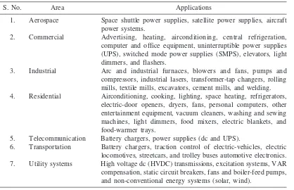
Table 1.1 shows some important applications of power electronics. The power ratings of power electronics systems range from a few watts in the case of lamps to several hundred megawatts in HVDC transmission systems.
Table 1.1 Some applications of power electronics
S. No. Area Applications
1. Aerospace Space shuttle power supplies, satellite power supplies, aircraft
power systems.
2. Commercial Advertising, heating, airconditioning, central refrigeration,
computer and office equipment, uninterruptible power supplies (UPS), switched mode power supplies (SMPS), elevators, light dimmers, and flashers.
3. Industrial Arc and industrial furnaces, blowers and fans, pumps and
compressors, industrial lasers, transformer-tap changers, rolling mills, textile mills, excavators, cement mills, and welding.
4. Residential Airconditioning, cooking, lighting, space heating, refrigerators,
electric-door openers, dryers, fans, personal computers, other entertainment equipment, vacuum cleaners, washing and sewing machines, light dimmers, food mixers, electric blankets, and food-warmer trays.
5. Telecommunication Battery chargers, power supplies (dc and UPS).
6. Transportation Battery chargers, traction control of electric-vehicles, electric
locomotives, streetcars, and trolley buses automotive electronics.
7. Utility systems High voltage dc (HVDC) transmissions, excitation systems, VAR
1.4
POWER SEMICONDUCTOR DEVICES AND THEIR
CLASSIFICATIONS
Ever since the silicon controlled rectifier (SCR), the first thyristor, came into existence late in the year 1957, a wide variety of power semiconductor devices were developed during the three decades that followed this invention. Until the year 1970, the SCR and other power semiconductor devices of the thyristor family such as TRIAC and DIAC had been exclusively used for power control applications in industries. The applications of other important power semiconductor devices that include power BJT, power MOSFET, and so forth to power control problems began in 1970.
Power semiconductor devices can be classified into three groups according to their degree of controllability. These groups have been briefly described here:
Group I includes uncontrolled power semiconductor devices such as diodes. These are called
uncontrolled devices because their ON and OFF states are not dependent on the control signals but on supply and load circuit conditions.
Group II devices are partially controllable. These include devices that are triggered into conduction by control signals but are turned off by the load circuit or by the supply. Such devices include thyristors such as line commutated SCR, force commutated SCR, light activated SCR, TRIAC, DIAC, and more.
Group III devices can be turned on and off by control signals. This category of fully controllable devices includes:
1. Power BJTs
2. Power MOSFETs
3. Insulated Gate Bipolar Transistors (IGBTs)
4. Gate Turn Off Thyristors (GTOs)
These devices are also referred to as gate controlled devices or gate commutation devices.
Group II and group III devices can also be classified—according to the gate signal requirements as under:
1. Pulsed gate requirements (SCR and GTO).
2. Continuous gate signal requirements (BJT, MOSFET, and IGBT).
The classification of the devices can also be done on the basis of voltage withstanding capability as under:
1. Unipolar voltage withstanding capability (BJT, MOSFET, and IGBT).
2. Bipolar voltage withstanding capability (SCR, GTO).
And on the basis of current conduction capability as under:
1. Unidirectional current capability (SCR, GTO, BJT, MOSFET, IGBT, and Diode).
2. Bidirectional current capability (TRIAC).
These devices may either be voltage controlled or current controlled. The voltage controlled devices are:
1. Power MOSFET
The current controlled devices are:
1. Thyristors 2. Power BJTs, etc.
The important features of these devices are summarized in Table 1.2
P
Table 1.2 Properties of power semiconductor switching devices
1.5
POWER SEMICONDUCTOR DEVICES: CHARACTERISTICS AND
RATINGS
A diode is a two-layer p-n junction semiconductor device with two terminals, namely anode and cathode. If a forward voltage that makes the anode potential greater than that of the cathode, is applied, the device starts conducting and behaves essentially as a closed switch. For a reverse voltage, the diode does not conduct but behaves as an open switch blocking the reverse voltage. Power diodes are of three types: general purpose, high speed (or fast recovery), and Schottky types.
General-purpose diodes are available up to 3000 V, 3500 A. They are useful for low frequency
applications since their reverse recovery times are comparatively large around 25 ms.
The fast-recovery type diodes with relatively small reverse recovery times (0.1–5 ms) are useful in high frequency circuits. The rating of fast recovery diodes can go up to 3000 V, 1000 A.
Schottky diodes have low on-state voltage drop and very small recovery time, typically nanoseconds. They are suitable for very high frequency circuits operating from low voltages. Their ratings are limited to 100 V, 300 A and the forward voltage drop of a power diode is very low, typically 0.3 V.
A thyristor has three terminals, namely an anode, a cathode, and a gate. Unlike the diode, which conducts only after its anode to cathode voltage exceeds the cut-in voltage, the thyristor will conduct only when a small current is passed through the gate terminal to the cathode. This means that the gate controls the beginning of conduction in thyristor. But once a thyristor attains the conduction state, the gate loses its control since the thyristor continues to conduct even after the removal of gate supply. When a thyristor is in a conduction mode, the forward voltage drop is very small, typically 0.5–2 V. A conducting thyristor can be turned off by making the potential of the anode equal to or less than the cathode potential. The line-commutated thyristors are turned off due to the sinusoidal nature of the input voltage and forced-commutated thyristors are turned off by an extra circuit employed called commutation circuitry. Natural or line-commutated thyristors are available with ratings up to 6000 V, 3500 A.
Light Activated SCRs (LASCR) are suitable for high voltage power systems especially HVDC.
They are available up to 6000 V, 1500 A with a switching speed of 200–400 ms.
GTOs are gate-turned-off thyristors. They are turned on by applying a short positive pulse to the gate as in SCRs but are turned off by the application of short negative pulse to their gates. Hence, these do not require any separate commutation circuit. GTOs are very attractive for forced commutation converters and are available up to 4000 V, 3000 A.
TRIACs are widely used in all types of simple heat controls, light controls, and in ac switches mostly in low power ac applications. The characteristics of TRIACs are similar to two thyristors connected in antiparallel and having only one gate terminal. The current flow through a TRIAC can be controlled in either direction.
A DIAC is a gateless TRIAC designed to breakdown at a low voltage.
Power MOSFETs are used in high-speed power converters and are available at a relatively low power rating in the range of 1000 V, 50 A at a frequency range of several tens of kilohertz. Power MOSFETs are voltage controlled devices unlike transistors that are current controlled. Similar to transistors that need continuous supply of base current to keep it in the ON state, MOSFETs also require the continuous application of gate source voltage of appropriate magnitude in order to remain in the ON state.
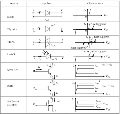
IGBTs are voltage-controlled power transistors. They are inherently faster than BJTs but not as fast as MOSFETs. They are suitable for high voltage and high current applications up to 1200 V, 400 A. They are acceptable to frequencies up to 20 kHz. Characteristics and symbols of important power devices are shown in Table 1.3.
VAK
A ID K
VAK ID
0
IA Gate triggered
IC
Table 1.3 Symbols and characteristics of important devices
V
GSn > VGS1
1.6
IDEAL AND REAL SWITCHES: COMPARISON OF
CHARACTERISTICS
An ideal switch is one that possesses ideal characteristics like zero resistance when ‘ON’ and infinite resistance when ‘OFF’. Further, the transitions from OFF to ON and the reverse is expected to take place instantaneously in an ideal switch. Practical or real switches exhibit a deviation from these ideal properties by having finite but very small ‘ON’ state resistances and finite but very large ‘OFF’ state resistances, and very small OFF and ON transition times.
Power semiconductor devices are used essentially as switching elements in most of the power converter circuits. They are ideal substitutes for mechanical switches. The performance of a switch is assessed by its behaviour under static as well as its dynamic conditions. If a switch remains in its OFF state or ON state it is said to be in static condition. A dynamic condition prevails in the switch when it is moving from one state to another. High power conversion efficiencies would result if these switches behave like ideal switches both under static as well as dynamic conditions.
1.6.1 Ideal Switch Characteristics
Following are the features of an ideal switch:
(a) ON state resistance = 0, leading to zero forward voltage drop while in conduction state.
(b) OFF state resistance = ¥, resulting in zero leakage current while blocking forward as well
as reverse voltages under OFF state.
(c) Capacity to conduct infinitely large current and to withstand infinitely large forward as well as reverse voltages.
(d) Ability to switch instantaneously from OFF to ON and from ON to OFF state. (e) No power requirement to control the switch.
(f) Easy control.
Above features ensure zero conduction loss and zero switching loss in an ideal switch, even if the switch handles large power at high voltage and high current conditions. While no real power semiconductor switches have these ideal properties, efforts are continuously made to take the real switch features closer to those of ideal switch.
1.6.2 Desirable Characteristics of a Real Switch
The desirable qualities of a real switch are:
(a) The device conducts large currents with negligibly small voltage drops across them. (b) They must be able to block high forward as well as reverse voltages when OFF with
negligibly small leakage currents.
(c) Very small turn ON and turn OFF times so that the device can operate at high frequencies. (d) Suitable for parallel and series operations under high current and high voltage conditions. (e) High operating temperatures.
(f) Long life.
1.6.3 Power Loss Characteristics of an Ideal Switch
across the switch is zero while “ON” and the current through the device is zero during “OFF” state. Further since the transitions from ON to OFF and OFF to ON are instantaneous the switching losses are also zero. Device voltage and current waveforms are shown in Fig. 1.1(a) for the ideal switch. Power loss in the switch is zero during ON state, OFF state and also during the transition from one state to the other. This is depicted in power loss waveform shown in Fig. 1.1(b).
t t
vsw isw
isw
Psw
Psw = 0
(a) (b)
Switch OFF Switch
ON
iswvsw
Fig. 1.1 Characteristics of an ideal switch: (a) voltage and current waveforms and (b) power loss.
1.6.4 Power Loss Characteristics in a Real Switch
Real power semiconductor switches suffer from very small conduction losses and switching losses due to non-ideal features like finite, though very small, ON state resistances and very small OFF state resistances. The switching times are also finite, though very small, of the order of microseconds. The switching losses become considerable portion of the total device losses in devices like power MOSFETs operating at very high frequencies.
A simple circuit employing a real switch is shown in Fig. 1.2(a). The switch is assumed to possess ideal static characteristics, so that there is no static ON state and OFF state losses. However, because of the non-ideal dynamic characteristics, there would be switching losses. The switch voltage and switch current waveforms are shown in Fig. 1.2(b). The switching loss curve is also shown in Fig. 1.2(b).
t1
(a) (b)
±
t2 t3 t4 t
v v
R V
vsw Psw isw
vsw Psw
isw
Psw vsw
SW
Fig. 1.2 Power loss in the real switch: (a) circuit and (b) voltage and current waveforms and power loss curve.
The switch of Fig. 1.2(a) is turned ON at t = t1.Prior to t = t1 the switch is in the forward blocking
state. During the turn-on operation that takes place from t1 to t2, the voltage across the switch reduces
zero to the static ON state value, I. The current waveform represents the instantaneous value of the switch current during the turn-on transition. During this period, there is power dissipation inside the switch. The instantaneous value of this power loss is given by the curve shown in Fig 1.2(b) as the product of the instantaneous values of voltage and current. Depending on the nature of the current and voltage waveforms, during the transition, the peak power can reach relatively large magnitudes. The energy dissipated in this turn-on process can be assumed to be equal to the area under power loss/power dissipation curve.
Turn-off switching operation takes place from t3 to t4 as shown in Fig 1.2(b). During this
transition, switch voltage rises from zero to V, (the supply voltage) as the current falls from I to zero.
Transition periods, Ton and Toff are not equal in power semiconductor switches though Toff is
generally larger.
The total energy, Jsw dissipated in a switching cycle is given by the sum of the areas under
power loss wave form during turn-on and turn-off. Therefore,
Jsw = Jon + Joff (1.1)
where Jon and Joff represent switching energy loss during turn-on and turn-off, respectively.
The average power loss in watts is given by
Psw = (Jon + Joff)f = Jswf (1.2)
‘f’, is the switching frequency in Hz.
If the linear variation is assumed for voltage and current waveforms during on and
turn-off transitions as shown in Fig. 1.4, an expression for Jon can be obtained as:
on on
Similarly, during turn-off,
off off 1 =
6
J VIt (1.4)
The total energy loss/cycle is equal to
sw on off
1
= ( )
6
J VI t t joules.
The average power loss or power dissipation due to switching losses is equal to:
sw on off
1
= ( )
6
P VI t t f
where ‘f’ is the switching frequency.
If the static performance of the switch is also non-ideal, i.e. ON-state resistance of the switch
is finite of the order of a few ohms, resulting in a small conduction voltage drop vf then, Jon, taking
into account the above voltage drop, vf,
on on on
1 1
6 3 f
J VIt V It (1.5)
A similar analysis for the turn-off period gives,
off off off
1 1
6 3 f
Therefore, the total energy loss/cycle is
The average switching power dissipation at a switching frequency f is given by
sw on off
ON-state power loss
The power loss during ON-state of the switch is calculated as follows:
For a given duty cycle k, ‘ON’ time of the switch is
The energy dissipation of the switch during its static ON-state in one switching cycle will be
on off
Therefore, the average static power dissipation at a frequency f will be
static on off
1
1.7
POWER ELECTRONIC SYSTEMS
The block diagram shown in Fig. 1.3 depicts a typical power electronic system. Major system components are shown in various blocks and an ac or a dc supply may be used as a main power source.
Main power source
Feedback signal
The output from the power electronic converter may be variable dc, or ac voltage, or it may be a variable voltage and variable frequency. In general, the output of a power electronic converter circuit depends upon the requirements of the load. For example, if the load is a dc motor, the converter output is a variable direct voltage. In case of an induction motor, the converter output is a variable voltage and variable frequency ac.
The feedback voltage signal may correspond to the speed if it were a rotating machine and it is then compared with the command signal. The difference of the two, when taken through the digital circuit components, controls the instant of turn-on of semiconductor devices forming the solid-state power converter system. In this manner, speed of the motor can be controlled, as desired, over a wide range with the adjustment of the command signal.
1.8
TYPES OF POWER ELECTRONIC CIRCUITS/CONVERTERS
Broadly speaking, power electronic converters (or circuits) can be classified into five types as:
1. Diode rectifiers: A diode rectifier circuit converts ac input voltage into a fixed dc voltage. The input may be single-phase voltage or a three-phase voltage. Diode rectifiers find wide use in electric traction, battery charging, electroplating, electrochemical processing, power supplies, welding, and uninterruptible power supply (UPS) systems.
2. AC to DC converters (Phase-controlled rectifiers): These converters translate constant ac voltage to variable dc output voltage. These rectifiers are also called line-commutated or naturally commutated ac to dc converters since these rectifiers use line voltage or source voltage for commutation. Phase-controlled converters use line-commutated thyristors. They may be 1-phase or 3-phase converters depending on the number of the input supply phases. These are used in dc drives, metallurgical and chemical industries, excitation systems for synchronous machines and so forth.
3. DC to DC converters (DC choppers): A dc chopper converts fixed dc input voltage to a variable dc output voltage. The chopper circuits use forced commutation. Thyristors are used in high power DC choppers. For low power applications, thyristors are replaced by power transistors, power MOSFETs, GTO thyristors, and the like. Choppers find a wide application in dc drives, subway cars, trolley trucks, battery-driven vehicles, and many more.
4. DC to AC converters (inverters): An inverter converts fixed dc voltage supply to ac voltage supply. The converters of this type use the principle of Pulse Width Modulation (PWM) to produce an output which may be a variable voltage and variable frequency supply. Modern day inverters use power semiconductor devices such as power transistors, power MOSFETs, and IGBTs. Forced-commutated inverters find wide use in induction-motor drives, synchronous induction-motor drives, induction heating, UPS, and so on. However, the inverters used in HVDC transmission are dependent on the supply voltage for their commutation. Hence, they are known as line-commutated inverters.
5. AC to AC converters: These convert fixed ac input voltage into variable ac output voltage. There are two types of ac to ac converters.
controller employs two thyristors in antiparallel or a single TRIAC. Turn-off is obtained by line commutation. Output voltage is controlled by varying the firing angle delay. AC voltage controllers are widely used to control heating and lighting, speed control of fans, pumps and so on.
(b) Cycloconverters: These circuits convert input power at one frequency directly to output power at a different frequency. (These are single stage converters). Line commutation is more common in these converters, though forced and load commutated cycloconverters are also available. These are primarily used in slow-speed large ac motors that drive loads like rotary kilns.
1.9
MERITS AND DEMERITS OF POWER ELECTRONIC CONVERTERS
Merits
1. High efficiency due to low loss in power semiconductor devices. 2. High reliability of power-electronic components and converter systems. 3. Long life and less maintenance due to the absence of moving parts. 4. Fast dynamic response compared to electromechanical converter systems.
5. Small size and less weight result in less floor space and therefore, lower installation cost. 6. Mass production of power semiconductor devices has brought down the cost of converter
equipments.
Demerits
Power-electronic converter circuits introduce harmonics into the supply and the load systems, adversely affecting the performance of the load and the supply. In the supply system, the harmonics distort the voltage waveform and seriously influence the performance of other equipments connected to the same supply line. In addition, the harmonics in the supply line can also cause interference with communication lines. It is, therefore, necessary to insert filters at the input of a converter. Other disadvantages of the converters include:
1. Ac to dc and ac to ac converters operate at a low input power factor under certain operating conditions. In order to avoid a low power factor, some special measures have to be adopted. 2. Power-electronic controllers have low overload capacity. These converters must, therefore, be rated for taking momentary overloads which increases the cost of power electronic controllers.
3. Regeneration of power is difficult in power electronic converter systems.
The merits possessed by power electronic converters far outweigh their disadvantages. As a consequence, semiconductor-based converters are being extensively employed in systems where power flow is to be regulated. As already stated, conventional power controllers used in many installations have already been replaced by semiconductor-based electronic controllers.
1.10
RECENT DEVELOPMENTS
the new circuits. It is easier to study the circuit using simulation compared to accomplishing the same in the laboratory on a hardware breadboard. Simulation packages such as SPICE and SABER are popular amongst power electronic engineers and academicians for their usefulness in the analysis, design, and education.
The demand for sophistication and growth for power electronics is expected to come from the following areas:
1. SMPS and UPS,
2. Energy conservation,
3. Process control and factory automation (Robotics),
4. Transportation,
5. Electro-technical applications such as welding, electroplating, and induction heating, and
6. Utility related applications, for example, HVDC.
Power electronic modules
A power electronic converter may require two, four, or more semiconductor devices depending upon the circuit configuration. Power modules consisting of two, four or six devices are, at present, available. Thus, a power electronic converter can be assembled from power modules instead of from individual semiconductor devices. Gate drive circuits for power modules are also commercially available. As a result of these developments, intelligent modules have come in the market.
Intelligent module, also called smart-power, is state-of-the-art power electronics and it consists of power module and a peripheral circuit. The peripheral circuit comprises an interface of power module with the input/output through proper isolation from low-voltage signal and high-voltage power circuit, a drive circuit, protection and diagnostic circuitry against maloperation such as excess current, over voltage and so on, microcomputer control, and controlled power supply. The user has merely to connect the existing supply and the load terminals to the smart-power. At present, intelligent modules are being used extensively in power electronics.
SUMMARY
SOLVED EXAMPLES
EXAMPLE 1.1 Typical switching waveforms for a real switch are given in Fig. 1.4. (i) Show that switch-on energy loss in this case is given by
on on
1 6
J VIt
where
V = OFF state voltage
I = ON state current
ton = Turn-ON time.
(ii) For the same switch, obtain the expression for the switch-off energy loss as
off off 1 6
J VIt
where toff = Turn-OFF time
(iii) Find the expression for average switching power loss.
(iv) Also obtain the expression for instantaneous peak power loss during switch-on and the instant, it occurs.
Solution
(i) Assume linear variation for voltage and current during ton and toff. The OFF-state voltage
is V and the ON-state current is I. The switching frequency is f Hz. The switch is ideal
as far as its static performance is considered, i.e. the switch conduction loss is zero as its ON-state resistance is zero. Figure 1.4 shows the voltage across the switch and the current through it as functions of time.
V V
I
t
ton toff
ISW
VSW
t
Fig. 1.4 Voltage and current waveforms (E 1.1). Energy loss during turn-on:
Taking t = 0, as the starting of turn-on proccess, v and i during turn-on are expressed as
on
It i
on
The instantaneous power will be
2
(ii) Energy loss during turn-off:
off
i The total energy loss due to switching in one cycle is:
on off
J J J
(iii) For a switching frequency f, the average power dissipation in the switch will be:
sw on off
1
( ) watts.
6
P VI t t f
(iv) To determine the instantaneous maximum power dissipation, during ton
2
Substituting for t,
2
Pmax, the instantaneous peak power loss occurs at
EXAMPLE 1.2 In case I = 80 A, V = 220 V, ton = 1.5 µs, and toff = 4 µs for switching waveforms shown in Fig. 1.4, find the energy loss during switch-on and switch-off intervals. Find also the average power loss in the switch for a switching frequency of 2 kHz.
Solution
on on
1 6
J VIt
=
6
6
220 80 1.5 10
4400 10 W-s
6
= 4.4 mW-s. (or) 4.4 mJ.
off off 1 6
J VIt
6
220 80 4 10
11.73 mJ 6
Average power loss = (4.4 + 11.73) × 2000 × 10–3
= 32.26 W.
EXAMPLE 1.3 In case I = 100 A, V = 200 V, ton = 1.5 µs and toff = 4 µs. Find peak instantaneous power dissipation.
Solution
Power dissipation,
max 4
100 200
4 5000 W.
VI P
EXAMPLE 1.4 Derive an expression for energy loss during turn-on transistion and turn-off
transistion for a switch whose V and I curves are given in Fig. 1.5. The switch is assumed to be
non-ideal both during static and dynamic conditions.
.
V
I
ton Vf toff t
Solution
A similar analysis will give, during toff,
off off off
1 1
6 3 f
J ÈÉ VIt V It ØÙ
Ê Ú
The total energy dissipation will be
on off on off
Switching power dissipation at a frequency f Hz is equal to
sw on off
EXAMPLE 1.5 Derive an expression for energy loss and power loss in the device during conduction, given the following data:
Turn-on time = Ton
Turn-off time = Toff
The switched duty cycle = k
Frequency = f
Solution
Taking Ton = static on time, Ts + ½ (ton + toff) Static ON-state duration of the switch is:
Ts= k
f – ½ (ton + toff) The energy dissipated during conduction is
REVIEW QUESTIONS
1.1 What is power electronics?
1.2 List the devices employed for power control prior to the advent of thyristors.
1.3 State the applications of power electronics in electric utility systems.
1.4 List the important gate controlled devices.
1.5 Give the symbol and characteristics of N-channel MOSFET.
1.6 What are the applications of inverters?
1.7 What are the applications of phase-controlled rectifiers?
1.8 List the features of an ideal switch.
1.9 List the characteristics of a real switch.
1.10 What are the advantages and disadvantages of power electronic converters?
1.11 How do the gating requirements differ between thyristor and transistor?
1.12 What is power electronic module?
1.13 What are the advantages and disadvantages of high frequency switching?
1.14 Describe smart power.
PROBLEMS
1.1 Transition times needed by a real switch are, ton = 2 µs and toff = 4 µs. The forward voltage
drop during ‘ON’ state is constant at 2 V, when the switch conducts a current of 10 A. The
OFF state voltage is 120 V. The switch has a repetitive switching frequency, f Hz. The
switching duty cycle, k = 0.6. Determine the frequency ‘f’ at which the switching power loss
begins to rise above the static conduction losses. What is the total power dissipation in the switch at this frequency? Assume linear variations for both voltage and current.
[Ans. 9.23 kHz, 22.9 W]
1.2 For the typical switching waveforms shown in Fig. 1.4 for a power semiconductor
switch:
(a) Find the expressions that give the peak instantaneous power loss during ton and toff
intervals, respectively.
(b) Calculate the peak values of instantaneous power loss during ton and toff given that on
state current is 50 A and off-state voltage is 200 V.
[Ans. (a)
4
VI
during ton as well as toff (b) 2500 W]
1.3 The switching characteristics for a power semiconductor device is as shown in Fig. 1.6.
Derive the expressions for energy loss during turn-on and turn-off periods, and also for the average switching loss. Sketch the variation of power loss during turn-on and turn-off
periods. For Vs= 220 V, Ia= 10 A, t1 = 1 µs, t2 = 2 µs, t3 = 1.5 µs and t4 = 3 µs, find the
average value of power switching loss in the device for a switching frequency of 1 kHz.
[Ans. 1
2VsIa(t1 + t2), 1
2VsIa(t3 + t4), 1
VS
Ia VS
t1 t2 ton
t3
toff t4
t Vs .Ia
20
Power Switching Devices
and Their Characteristics
22222
2.1
PRELIMINARIES
An overview of important power semiconductor devices and their essential characteristics has been provided in section 1.4 of Chapter 1. Power semiconductor devices such as power diodes and power transistors are more complex in structure and operation when compared to their low power counter-parts, signal diodes, and signal transistors with more than the usual number of p-n layers to handle higher voltages and currents. These devices can be broadly classified into two groups. One group is the one that contains thyristors, the earliest and the most popular amongst them being SCR (Silicon Controlled Rectifier). The other group contains power diodes and members of the power transistor family. The devices in thyristor family include silicon controlled rectifier (SCR), TRIAC, DIAC, LASCR, GTO thyristor, programmable UJT, silicon unilateral switch, asymmetrical thyristor, and reverse conducting thyristor, and so on. The power transistor group comprises in addition to diodes, bipolar junction transistors (BJTs), metal oxide semiconductor field effect transistors (MOSFETs), and insulated gate bipolar transistors (IGBTs). Alternately, these devices can be classified into three groups based on the degree of controllability as:
Diodes: Uncontrolled since ON and OFF states are controlled by the power circuits.
Thyristors: Turned ON by control signal but turned OFF by the power circuit. GTO thyristor is an exception.
Controllable switches: Turned ON and turned OFF by control signals. BJT, MOSFET, IGBT, MCT and the like come under this category in which GTO thyristor can also be included.
This chapter devotes itself to the study of the constructional features, characteristics, and working of various power semiconductor devices. The ratings and protection methods of these devices are also covered in some detail.
2.2
POWER DIODES
functions such as freewheeling of energy in inductive circuits, charge reversal in capacitors, and trapped energy recovery in addition to the main function of rectification. Power diode is a two-layer, two terminal, p-n junction semiconductor device. It has one p-n junction formed by alloying, diffusing, or epitaxial growth. The two terminals of diode are called anode and cathode, refer Fig. 2.1(a). Two important characteristics of power diodes, namely the V–I characteristics and the reverse recovery characteristics are now described.
Fig. 2.1 (a) p-n junction, (b) diode equivalent circuit, (c) V–I characteristics.
2.2.1 Diode V–I Characteristics
The V–I characteristics of a diode whose equivalent circuit is depicted in Fig. 2.1(c) are discussed
in this subsection. The source voltage VS forward biases the p-n junction by making the anode
positive with respect to cathode.
The characteristics under forward biased condition appear in the first quadrant of the voltage
versus current plot. The diode current starts from zero and increases gradually for low values of VS.
However, it starts to rise rapidly for voltages above cut-in or threshold voltage, (0.7 V for silicon diodes) as shown in Fig. 2.1(c). The diode is then in conduction state and the voltage drop in the device is about 1 V and the conduction losses are, therefore, low.
The characteristics under reverse biased condition appear in the third quadrant. The reverse current is very small, of the order of micro or milliamperes depending on the device ratings and it increases gradually with increasing reverse bias voltage. For a particular reverse voltage, the junction breaks down allowing large reverse current to flow. As both the breakdown voltage and the breakdown current are large, increased power dissipation occurs in the device. This causes further increase in the diode reverse current which will ultimately destroy the device. This reverse avalanche breakdown of a diode is avoided by operating the diode below the specified peak
repetitive reverse voltage VRRM. Figure 2.1(c) illustrates diode characteristics where VRRM and cut-in
voltage are indicated.
Diode manufacturers also indicate the value of peak inverse voltage (PIV) of a diode. This is the largest reverse voltage to which a diode may be subjected during its working. PIV is the same
as VRRM. The power diodes are now available with forward current rating of 1 A to several thousands
of amperes and with reverse voltage ratings of 50 V to 3000 V or more.
(a) (b) (c)
p n Cathode Anode
i
VS VS
i D
Cathode Anode
I
VS Forward voltage drop
Forward characteristics
Cut-in voltage = 0.7 V Reverse
ta tb trr
t If
if
0
IRM IRM
t 0
vf vf
t Power
loss in diode
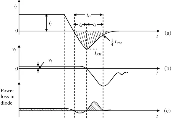
2.2.2 Diode Reverse Recovery Characteristics
If the circuit conditions require the diode to switch off, the forward diode current first decays to zero and then the diode continues to conduct in the reverse direction as shown in Fig. 2.2(a). This is caused by the stored charges in the two layers of the diode. The time duration for which reverse
current flows in the device is called reverse recovery time trr. During reverse current flow, the charge
carriers stored in the device at the end of conduction are removed. The device does not attain its full blocking capability unless and until stored charges are completely removed from the layers.
The reverse recovery time trr is composed of two segments of time ta and tb, that is,
trr = ta + tb
Time ta, marked in Fig. 2.2(a), is the time required for the reverse recovery current to attain
its maximum value IRM from zero. During this time ta, the charge stored in depletion region is
removed. Time tb is the time required for the reverse current to fall to 25% of its peak value from
its peak value IRM. The shaded area in Fig. 2.2(a) represents the stored charge or reverse recovery
charge. In Fig. 2.2(b), the waveform of forward voltage drop vf across the diode is also shown. The
power loss during this reverse recovery process which is the product of vf and if is also depicted in
Fig. 2.2(c).
(a)
(b)
(c)
The average value of vf If gives the total power loss in a diode. The major power loss in the diode
occurs during the period tb.
2.2.3 Types and Ratings of Power Diodes
Diodes are classified according to their reverse recovery characteristics. Three types of these power diodes are:
Fig. 2.2 Reverse recovery characteristics: (a) variation of forward current If, (b) forward voltage
drop vf and (c) power loss in diode.
(a) General-purpose diodes (b) Fast-recovery diodes (c) Schottky diodes
General-purpose diodes
These diodes have relatively large reverse recovery times, of the order of about 25ms. Their current
ratings vary from 1 A to several thousand amperes and the range of voltage rating is from 50 V to about 5 kV. Applications of power diodes of this type include battery charging, electric traction, electroplating, welding, and UPS.
Fast-recovery diodes
The diodes with low reverse recovery time, of about 5 ms or less, are classified as fast-recovery
diodes. These are used in chopper circuits, commutation circuits, switched mode power supplies, induction heating, and so forth. Their current ratings vary from about 1 A to several thousand amperes and voltage ratings from 50 V to about 3 kV.
For voltage ratings below about 400 V, the epitaxy is used for diode fabrication. These diodes have fast recovery time, as low as 50 ns. For voltage ratings above about 400 V, diffusion technique is used in the diode fabrication. In order to reduce the reverse-recovery time, platinum or gold doping may be carried out. But this doping increases the forward voltage drop in a diode.
Schottky diodes
This class of diodes uses metal-to-semiconductor junction for rectification purposes instead of p-n junction. Schottky diodes are characterized by very fast reverse recovery time and low forward voltage drop. Rectified current flow is by majority carriers only and this avoids the turn-off delay accompanied with minority carrier recombination. Their reverse voltage ratings are limited to about 100 V and forward current ratings vary from 1–300 A. The Schottky diodes are ideal for low voltage and high current DC power supplies.
2.2.4 Series and Parallel Operation of Diodes
In many high voltage applications such as HVDC transmission systems, a single commercially available diode may not possess the required voltage rating and therefore, adequate number of diodes are connected in series to obtain the required reverse voltage blocking capabilities. For similar reasons, diodes are connected in parallel to increase the current carrying capabilities to meet the desired current requirements. Therefore, in high voltage and high current circuits, the common practice is to use series-parallel connections of diodes. In the case of series connected diodes, blocking voltages of individual diodes under reverse biased conditions differ significantly. In the same manner, the parallel-connected diodes do not share the total current equally because of unequal forward resistances. Equal voltage sharing among diodes under reverse blocking conditions is achieved by connecting a resistor across each diode. But the voltage sharing under transient conditions is taken care of by capacitors connected across the diodes. Series diodes with voltage
sharing networks are shown in Fig. 2.3. Resistance Rs is used to limit the rate of rise of the blocking
voltage. Similarly, the current sharing can be equalized by adding series resistances and inductances
as shown in the Fig. 2.3(b). The resistors R1 and R2 help proper current sharing under steady-state
2.3
THYRISTORS
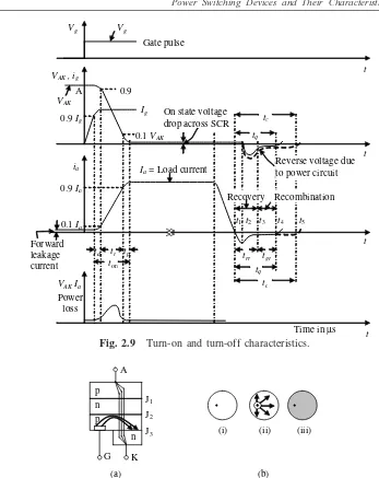
Silicon controlled rectifier (SCR) being the first amongst the thyristor family of four-layer devices is frequently and often loosely referred as thyristor. While it shares the rectifying property of a diode, it differs in its capability to block the forward biasing voltage until the gate receives the triggering signal. Thus, SCR is a device with control over turn-on while its turn-off is determined by the circuit voltages and parameters.
2.3.1 Structure, Symbol, and V–I Characteristics
It is a four-layer (p-n-p-n), three junction (J1, J2, J3) power semiconductor (silicon) device having
three terminals namely anode (A), cathode (K), and gate (G). The structure and symbol of the thyristor are shown in Fig. 2.4. Anode is connected to the outer p layer, the cathode is connected
to the outer n layer and the gate is connected to the inner p layer. J1, J2, and J3 are the three junctions
marked as shown in Fig. 2.4(a). The constructional details of a typical thyristor are shown in Fig. 2.4(b). The schematic diagram and circuit symbol are shown in Figs. 2.4(a) and (c) respectively. The SCR exhibits the property of a switch as it possesses only two stable states, that is, ON and OFF
states. During ON state, the device offers very low resistance, as small as 1W but during the OFF
state, the device offers a very high resistance, as large as 10 MW. The static V–I characteristics of
a thyristor is shown in Fig. 2.5 for different gate currents. Here, VAK is the voltage across the thyristor
terminals and IAK is the anode current.
Fig. 2.3 (a) Series operation, (b) parallel operation.
Fig. 2.4 (a) Schematic diagram, (b) constructional details and (c) circuit symbol.
p
Static V–I characteristics of a thyristor
The circuit diagram representing the connections to be made for experimentally obtaining static V–I characteristics of a thyristor is shown in Fig. 2.5(a). The anode and cathode are connected to
main source VSthrough variable resistance load. The gate and cathode are fed from a source VgS that
provides positive gate current from gate to cathode.
The thyristor has three basic modes of operation, namely forward blocking mode (OFF state), reverse blocking mode (OFF state), and forward conduction (ON state) mode as revealed by the V-I characteristics.
Forward blocking mode: A thyristor remains in forward blocking mode if its anode to cathode voltage is positive but the gate signal is insufficient or absent. It is seen from Fig. 2.6(a) that
junctions J1 and J3 are forward biased but junction J2 is reverse biased. Also a small leakage current
Fig. 2.5 (a) Circuit connections and (b) V–I characteristics.
p
Fig. 2.6 (a) Forward blocking mode and (b) reverse blocking mode.
+
Reverse leakage current Forward conduction state
(on state)
Latching current Holding current
(b)
Volts