DESIGN AND MODELLING OF CONVERTER FOR WAVE ENERGY
by
Naily Akmal Binti Mohd Zamri 14516
Supervisor Dr. Taib Bin Ibrahim
Dissertation submitted in partial fulfilment of the requirements for the
Bachelor of Engineering (Hons) (Electrical and Electronic)
SEPTEMBER 2014
Universiti Teknologi PETRONAS Bandar Seri Iskandar
31750 Tronoh
Perak Darul Ridzuan
i
CERTIFICATION OF APPROVAL
DESIGN AND MODELLING OF CONVERTER FOR WAVE ENERGY
by
Naily Akmal Binti Mohd Zamri
A project dissertation submitted to the Department of Electrical & Electronic Engineering
Universiti Teknologi PETRONAS in partial fulfilment of the requirement for the
Bachelor of Engineering (Hons) (Electrical & Electronic Engineering)
Approved by
__________________________
Dr. Taib Bin Ibrahim Project Supervisor
UNIVERSITI TEKNOLOGI PETRONAS TRONOH, PERAK
September 2014
ii
CERTIFICATION OF ORIGINALITY
This is to certify that I am responsible for the work submitted in this project, that the original work is my own except as specified in the references and acknowledgements, and that the original work contained herein have not been undertaken or done by unspecified sources or persons.
__________________________
Naily Akmal Binti Mohd Zamri
iii
ABSTRACT
World energy consumption is increasing by year. This fact has led to extensive researches conducted in utilizing renewable energy all around the world as the alternative. Wave energy is one of the alternative energies that have high potential to be developed. However because of the nature of ocean wave which is random in term of amplitude and frequency, the generated voltage from Wave Energy Converter (WEC) will be non-uniform and unstable. This non-uniform voltage output from WEC cannot be directly used and thus an intermediate system between the WEC and load is needed. This project entitled “Design and Modelling of Converter for Wave Energy” is focusing on developing the intermediate system which is voltage conversion system. It aims to design wave energy converter in stabilizing the output voltage from the generator so that it is suitable to be used with load and at the same time conduct extensive literature review on the previous technologies. WEC that will be considered in this project is Resen Wave LOPF Buoy that is available in UTP Offshore Lab with the maximum output AC voltage of 15 V. Literature review is conducted onto the type of converters that can be implemented to convert AC voltage. From the study carried out, AC-DC-AC converter is the most suitable converter type to be used with renewable energy. Next, extensive literature review on three previous technologies has also been completed and from the review done; a proposed design of converter is introduced. The proposed converter design is designed based on one of the previous technologies reviewed with several changes carried out to improve the system and to make the converter suitable to be used with the specified WEC in this project. The proposed design is modelled in MATLAB simulink and it is simulated to acquire the output voltage from the designed converter. Other than the final output voltage from converter, the DC voltage output from the rectifier is also being analysed. The output voltage is also being compared with the result from the previous technology. From the results obtained, it can be concluded that using the proposed converter design voltage from the generator is able to be stabilized and thus achieved the objective of this project. Future work can be conducted in term of controlling scheme for current stabilizing and designing for the full scale system to be integrated with the grid.
iv
ACKNOLEDGEMENT
رلأ ﻳﹺﺣﱠ
مﹺ ﹺﻥﹶﻤﹾﺣﱠﺭﹾﻠ للەأ أ ﹺ ﹾﺴﹺﺒ مﹺ
With the Name of Allah the Most Gracious, the Most Merciful
First and foremost, I would like to praise and thanks Allah S.W.T that with His blessings and the strength He granted me, I am able to complete my final year project (FYP) entitled “Design and Modelling of Converter for Wave Energy”. These two semesters of completing this project were full with ups and downs that dependence onto Him is among others that make me persistent until the last phase.
My utmost gratitude goes to my supervisor; Dr. Taib bin Ibrahim for his support and guidance throughout the project execution. His full commitment in supervising and also giving motivation has been very significant to me. Other than that, I would also thanks my sponsor which is Majlis Amanah Rakyat (MARA) that has been providing sponsorship throughout my five years of study in UTP.
My appreciation also goes to my fellow members, Nur Farahin Zulkarnain, Muhammad Faris Muhamad Na’afi and Nurul Shuhadah Md. Zim, who have been carrying out FYP under Dr. Taib’s supervision as well. Even though all of us were conducting different projects, being under supervision of Dr. Taib, we have been very supporting to each other and at certain point we even know the current progress and issues faced by each of the members. Not to forget, my classmates from Electrical and Electronic Department that somehow have assisted me directly or indirectly throughout the process of completing the project.
Lastly, to my parents, Mohd Zamri Mohd Nasir and Rusilah Ismail who are very supportive, their encouragement and motivation has been one of the keys that strengthen me in enduring these two semesters.
v
TABLE OF CONTENT
ABSTRACT ... iii
ACKNOLEDGEMENT ... iv
TABLE OF CONTENT ... v
LIST OF TABLE ... vii
LIST OF FIGURE ... viii
ABBREVIATIONS AND NOMENCLATURES ... x
CHAPTER 1 INTRODUCTION ... 1
1.0 INTRODUCTION ... 1
1.1 PROJECT BACKGROUND ... 1
1.2 PROBLEM STATEMENT ... 3
1.3 OBJECTIVES OF STUDY ... 3
1.4 SCOPE OF STUDY ... 4
1.5 CONCLUSION ... 4
CHAPTER 2 LITERATURE REVIEW ... 5
2.0 INTRODUCTION ... 5
2.1 DIFFERENT TYPE OF CONVERTERS ... 5
2.1.1 Direct AC-AC converter ... 5
2.1.2 AC-DC-AC converter ... 6
2.2 PREVIOUS TECHNOLOGIES FOR WAVE ENERGY CONVERTER .... 6
2.3 DC VOLTAGE REGULATION ... 9
2.4 VOLTAGE CONVERTER PROPOSED DESIGN ... 10
2.5 CONCLUSION ... 14
CHAPTER 3 METHODOLOGY ... 15
vi
3.0 INTRODUCTION ... 15
3.1 PROJECT ACTIVITIES ... 15
3.1.1 Literature Review ... 16
3.1.2 Designing Converter ... 16
3.1.3 Simulation of the Designed Converter... 16
3.2 TOOLS ... 17
3.2.1 Wave Generator ... 17
3.2.2 Simulink MATLAB ... 18
3.3 PROJECT SCHEDULE ... 18
3.4 CONCLUSION ... 18
CHAPTER 4 RESULT & DISCUSSION ... 19
4.0 INTRODUCTION ... 19
4.1 SIMULATION RESULT FROM MATLAB SIMULINK ... 19
4.2 DISCUSSION ... 26
4.3 CONCLUSION ... 29
CHAPTER 5 CONCLUSION AND RECOMMENDATION ... 30
REEFERENCES ... 32
APPENDICES ... 35
Appendix 1 Project Gantt chart and Key Milestones for FYP 1 ... 35
Appendix 2 Project Gantt chart and Key Milestones for FYP ... 36
vii
LIST OF TABLE
TABLE 1. Advantage and Disadvantages of Previous Technologies ... 11 TABLE 2. Summary of Output Parameter ... 25 TABLE 3. Comparison of Output of Proposed Design and Design by Muller, Kouro, et al. ... 28
viii
LIST OF FIGURE
FIGURE 1. World Electricity Domestic Consumption from 1990 to 2012 ... 1
FIGURE 2. World Wave Power Availability in kW/m of Wave front ... 2
FIGURE 3. Malaysia Wave Power Availability in kW/m ... 2
FIGURE 4. Block Diagram for AC/DC/AC converter ... 6
FIGURE 5. Power Converter by Ran, Mueller, Ng, et al. ... 7
FIGURE 6. Back-to-back converter Configuration ... 8
FIGURE 7. Wave Energy Converter Configuration ... 9
FIGURE 8. Basic Circuit Connection of Zener Diode ... 10
FIGURE 9. Discrete Transistor Voltage Regulator ... 10
FIGURE 10. Block Diagram of the Proposed Design ... 12
FIGURE 11. Three Phase Thyristor Rectifier ... 12
FIGURE 12. Circuit at Inverter Side... 13
FIGURE 13. Improvised Circuit ... 13
FIGURE 14. Block Diagram of Finalized Proposed Design of Converter ... 14
FIGURE 15. Circuit of Finalized Proposed Design of Converter ... 14
FIGURE 16. Project Flow ... 15
FIGURE 17. Input Wave Signal and Generator Model in MATLAB ... 17
FIGURE 18. The Circuit of Input Wave with Modified Magnetic Flux Value ... 17
FIGURE 19. Real Wave Signal from Wave Generation Model ... 19
FIGURE 20. Three Phase Voltage Output from Generator ... 20
FIGURE 21. Output Voltage at DC Link of Original Proposed Circuit ... 21
FIGURE 22. Voltage Output at DC Link of Improvised Design ... 22
FIGURE 23. Output Line to Line Voltage from Inverter of Proposed Circuit ... 23
ix
FIGURE 24. Output Phase A Current from Inverter of Proposed Circuit ... 24
FIGURE 25. Zener Diode Characteristic ... 26
FIGURE 26. Rectified DC Voltage by Muller, Kouro, et al. ... 27
FIGURE 27. Line to Line Output Voltage of design by by Muller, Kouro, et al. ... 27
x
ABBREVIATIONS AND NOMENCLATURES
AC Alternating Current
DC Direct Current
FYP Final Year Project
Hz Hertz
IGBT Insulated-gate bipolar transistor
LV Low voltage
MOSFET Metal-oxide-semiconductor field-effect transistor
MV Medium voltage
NPC Neutral point clamp
PWM Pulse Width Modulation
TW Terawatt
TWh Terawatt-hour
WEC Wave Energy Converter
VSC Voltage Source Converters
1
CHAPTER 1 INTRODUCTION
1.0 INTRODUCTION
Chapter 1 provides an overview of the project in the big picture. This chapter outlines the need of alternative energy to sustain the increasing electricity consumption year by year. Other than that, it also discusses wave energy’s potential as alternative energy. Next, explanation is provided in this chapter in term of the problem found in electricity conversion of wave energy which led to the requirement of voltage conversion. Lastly, chapter 1 also presents the objectives outlined in this project and its scope of study.
1.1 PROJECT BACKGROUND
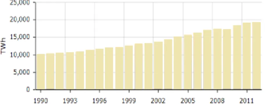
World electricity consumption is growing over the years. In year 2012, 19 461 TWh of world electricity domestic consumption was recorded in which it indicates 2.14%
increment from the year before [1]. This growth in world electricity consumption and also in the projected energy [1] demand as in [2] has led to vast researches conducted in the exploitation of renewable energies as an alternative to fossil fuel in serving the demand.
FIGURE 1. World Electricity Domestic Consumption from Year 1990 to Year 2012
2
Wave energy is renewable energy which has high potential to be developed as one of the main energy provider. 10 TW of total wave energy resource is estimated to be available in the open sea all around the world [3] and these resources are enough to provide electricity up to 2 TW [4]. Figure 2 and Figure 3 show the wave power availability all around the world and in Malaysia. In addition, wave activity is highly reliable and predictable in which its gradual activity’s variability and considerable warning, make the issues of grid disturbance manageable [5].
FIGURE 2. World Wave Power Availability in kW/m of Wave front [5]
FIGURE 3. Malaysia Wave Power Availability in kW/m [6]
Currently, large number of Wave Energy Converter (WEC) prototype and design is developed [7], [8], [9]. Nonetheless the exploitation of wave energy as the
3
resources of the current energy supplier is still unclear and in infant stage [8], [9], [10].
The method of maximum energy extraction from the WEC has still being the main concern that an efficient power conversion method is needed. The inconsistent voltage and frequency produced by the generator in WEC due to the varying speed of the translator require the voltage to be converted before being used smoothly with maximum efficiency of energy conversion [3], [8].
This project is being conducted to design a conversion system in stabilizing the output voltage from WEC. It focuses on designing and modelling of voltage conversion system for the output voltage and frequency of WEC. The designed converter shall be simulated using Simulink MATLAB software. The maximum voltage output from the generator is 15 V to 12 V. The input of the converter shall be limited to the wave generated with maximum amplitude of 1.5 m and range of frequency from 0.03 to 2.0 Hz.
1.2 PROBLEM STATEMENT
The nature of wave which has non-uniform frequency and amplitude will cause the varying in speed of the translator of WEC system. This in consequence affects the output voltage of the generator to be unstable. The unstable output from the generator will not be able to be directly utilized and thus a conversion system needs to be integrated to stabilize the output and consequently enable maximum extraction of wave energy from WEC system.
1.3 OBJECTIVES OF STUDY
The main objective of this project is;
i) To design wave energy converter in stabilizing the output voltage and frequency from WEC.
The associated objectives of this project are;
i) To conduct extensive literature review for the available technologies.
ii) To conduct simulation on the proposed wave energy converter design.
4 1.4 SCOPE OF STUDY
Chapter 1 of this paper discusses on the project background which lead to the identification of the problem statement and the significant of the project. Thorough explanation is provided to show the need of voltage conversion system in generating electricity from wave energy. Objectives of the project are also outlined to give clear view on the expected outcome of this project.
In chapter 2, the type of converters to be used in this project is reviewed. In addition, this chapter also highlights the discussion on previous technologies of voltage converter. This is significant for the development of the converter for this project which be based on the previous technologies reviewed. Lastly, the proposed design of the converter is introduced in this chapter.
Chapter 3 focuses on introducing the methodology taken to approach the project. Project activities, timeline and tools are outlined in this chapter.
Chapter 4 provides the results of the project acquired from the simulation of the proposed design. The results are discussed and analysed. This chapter is significant to point out either the project’s objectives are achieved or not.
Lastly, Chapter 5 covers the conclusion of the overall project and recommendation for future work is also stated in this chapter.
1.5 CONCLUSION
From the overview discussed in Chapter 1, it can be concluded that in utilizing wave energy as source of electricity, power conversion to stabilize the output voltage from the generator before feeding the energy to utilization is still in development status.
Hence, study on the optimized design is required to be performed. The next chapter will discuss on the review of the related literatures in providing the foundation to the project.
5
CHAPTER 2
LITERATURE REVIEW
2.0 INTRODUCTION
Chapter 2 provides review on the past researches and studies related to the project.
The review focuses on type of converters in power electronics, previous technologies for wave energy converter and the DC voltage regulator. The type of converters are reviewed in order to decide on which topology best to be used in this project while previous technologies are significant to provide basis for the design. In this chapter, three previous technologies are discusses together with their advantages and disadvantages. Lastly, this chapter also introduces the proposed design of the converter to be used in this project.
2.1 DIFFERENT TYPE OF CONVERTERS
In power electronics, AC power conversion can utilizes two types of conversion which are direct AC/AC converter and AC/DC/AC converter [11]. Both of the conversion types have several methods of implementation to achieve the power conversion.
2.1.1 Direct AC-AC converter
AC power is directly converted to another level of AC power using direct AC/AC converter. This type of power conversion method utilizes less circuit in series connection compared to the AC/DC/AC converter that in return lead to lesser conversion loses [12]. AC/AC converters can be achieved by implementing three methods which are Voltage Regulation (VR) converter, Cycloconverter and Matrix converter [11].
Even though, AC/AC converter is expected to have simpler circuit, this type of conversion method is not suitable to convert unstable AC output from the
6
renewable energy conversion system as the input of AC/AC converters are generally from the stable AC input [11].
2.1.2 AC-DC-AC converter
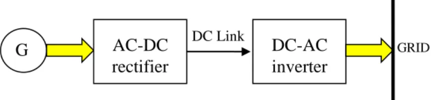
This AC-DC-AC converter is built up from several circuit connected together in series. AC-DC-AC converter is either of AC-DC converter proceeded directly by inverter or the rectifier is connected first to DC-DC converter and subsequently connected to an inverter [11]. The input of this type of converter can be from random input AC voltage. The converter can absorb the energy and transform it to a fixed DC link voltage [11] by utilizing AC-DC conversion. The energy from DC link voltage will be further transform to the required output in form of AC with modifiable voltage and frequency using DC-AC conversion [11].
There are many methods of implementation for this type of converter [8], [11], [13]. Among the methods are AC-DC-AC boost-type converter and three-level AC-DC-AC ZSI as in [8], [11], and three-level AC-DC-AC sparse matrix converter as in [13]. As random AC voltage could be fed to the input of AC-DC-AC converter, this converter is suitable to be used for renewable energy power conversion.
FIGURE 4. Block Diagram for AC/DC/AC converter
2.2 PREVIOUS TECHNOLOGIES FOR WAVE ENERGY CONVERTER Converters from three literatures [8], [3], [14] are discussed in this section. These three literatures implement AC/DC/AC conversion method to convert the unstable output from generator before feeding to the grid.
Ran, Mueller, Ng, et al. [8] highlights the application of single-phase boost rectifier instead of three-phase as being used in others as [3], [14]. The boost rectifier is being coupled to each machine coil instead of coupled the whole three-phase
G AC-DC
rectifier
DC Link
DC-AC inverter
GRID
7
system to three-phase rectifier. Each rectification from the coils is then being paralleled at the DC Link point. The researchers proposed this method as the coils that were connected in series forming the three phases lead to higher total resistance that is poor for low voltage and high-current machine. This happen as in certain translator arrangements, the stator end coils are possible to become inactive [8].
Metal-oxide-semiconductor field-effect transistor (MOSFET) is used as controlling part for the waveform of the current from the coil.
Unidirectional boost DC-DC converter is implemented in regulating the DC link voltage at the LV part [8]. Insulated-gate bipolar transistor (IGBT) is applied in the converter due to the DC link voltage’s magnitude at the inverter output.
However, in this paper, the DC-AC inverter has not been discussed in detail.
Ran, Mueller, Ng, et al. [8] proposed a converter that is equipped with several advantages which are it allows independent control of current drawn from each coil of the stator, it reduces total resistance than connected in 3 phase and it is less complex than utilizing 3 phase with anti parallel thyristor pair. However, there are a few disadvantages found in the topology which are it required utilization of huge number of circuit (48 circuits are required than 16 circuits in 3-phase) and it is only reasonable to be implemented in linear direct drive generator.
FIGURE 5. Power Converter by Ran, Mueller, Ng, et al. [8]
Wu, Ju, et al. proposed a power conditioning scheme [3] that is for Archimedes Wave Swing utilizes full-capacity back-to-back converter. This
8
converter configuration is made up of two controlled Voltage Source Converters (VSC) that is connected to a capacitor. One of the VSCs is at the generator side while another is connected to the grid side. The capacitor becomes the DC link and acts as the power storage as well as voltage source for the converters [3]. Wu, Ju, et al. [3]
outlined the main advantage of the design they proposed in which it reduces the dimension of capacitor by introducing Battery Energy Storage however it has limitation which is the controlling scheme is only valid under regular wave condition.
FIGURE 6. Back-to-back converter Configuration [3]
Lastly, Muller, Kouro, et al. [14] proposed to use diode full bridge rectifier.
This is due to the application of the power conversion is associated with Permanent Magnet Synchronous Generator which is unidirectional in the power flow and do not consume reactive power [14]. Implementing bridge rectifier is thus more cost effective even though it does not contain any control scheme. DC-DC converter shall be needed to counter the controlling part. Boost converter is used as the DC-DC converter [14] and depending on the rating of the generator; boost converter could be substituted with interleaved or multichannel boost converter. The boost converter functioning as the controlling part for voltage elevation in maintaining the ratio of the dc output from rectifier which is varying and the dc voltage at the converter at the grid side which is fixed [14].
Group of 8 or 12 power generation unit with DC-DC converter will be connected to a capacitor as the DC link which will then being connected to neutral point clamped converter (NPC) that acts as the inverter [14]. NPC is a three-level VSC suitable form medium voltage (MV) operation and it utilizes IGBT or MV- IGBT.
9
The design introduced by Muller, Kouro, et al. [14], has advantages in term of cost effectiveness as it only utilize diodes and also the output level which enable to be in 3 level. Other than that, it also lowers the transformer ratio at the grid side. In term of drawback, the design reduces control degree of freedom and introduce higher torque ripple
FIGURE 7. Wave Energy Converter Configuration [14]
2.3 DC VOLTAGE REGULATION
The voltage output of the DC link from the rectification will be DC voltage which is expected to be changing in term of the voltage level according to the non uniform input from the AC voltage. DC voltage regulation will be required to regulate the voltage at the DC link to be at one level [19]. There are several voltage regulators that can be implemented to achieve the regulation.
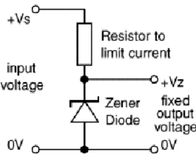
First method is by implementing zener diode as limiting elements [19]. Zener diode is designed to maintain fixed voltage across the load as it has breakdown properties that when they are biased by voltage higher than its breakdown voltage in reverse direction, it will maintain the breakdown voltage its own [20]. The basic circuit implementation of zener diode is as in Figure 8.
10
FIGURE 8. Basic Circuit Connection of Zener Diode
Another type of voltage regulator is discrete transistor [20]. The block diagram of voltage regulator is as in Figure 9. The regulator functions as the control element collects the input and receives feedback from the comparator circuit before outputting the voltage. The comparator takes data from the output voltage and compare with the reference voltage before feeding to the control elements. In this mechanism, the circuit able to maintain the output voltage at the desired level by taking sample from the current output for error correction in the control block.
FIGURE 9. Discrete Transistor Voltage Regulator
2.4 VOLTAGE CONVERTER PROPOSED DESIGN
Based on the literature review conducted, several advantages and disadvantages can be observed in the previous design of converter. The advantages and disadvantages of the designs reviewed are summarized as Table 1.
11
TABLE 1. Advantage and Disadvantages of Previous Technologies of Wave Converter
Design Advantage(s) Disadvantages(s)
Ran, Mueller, Ng, et al. [8] 1) Permit independent control of current drawn from each coil of the stator 2) Reduce total resistance than connected in 3 phase 3) Less complex than
utilizing 3 phase with anti parallel thyristor pair
1) Require utilization of huge number of circuit (48 circuits are required than 16 circuits in 3- phase)
2) Reasonable to be implemented in linear direct drive generator
Wu, Ju, et al. [3] 1) Reduce the dimension of capacitor by introducing Battery Energy Storage
1) The controlling scheme is only valid under regular wave condition Muller, Kouro, et al. [14] 1) Cost effective
2) Enable the output of 3 level voltage
3) Lower the transformer ratio at the grid side
1) Reduce control degree of freedom and introduce higher torque ripple 2) Grid side suitable for
Medium Voltage system
From the table, it is concluded that design by Muller, Kouro, et al. [14] is the previous design which is most reasonable with the scope of study of this paper.
However, due to utilization of diode bridge rectifier in the design, it leads to the presence of the drawback as mentioned in Table 1. Thus, for the design of this project, the generator side converter is changed from diode bridge rectifier connected to DC-DC converter to be a fully controlled converter utilizing thyristor in replace of the diode without DC-DC converter. The converter at the inverter side shall be replaced with universal IGBT bridge inverter circuit with PWM generator to accommodate the low voltage of the system. Figure 10 shows the original proposed block diagram of the wave energy converter design while Figure 11 and Figure 12 show the full circuit of each of the block diagram.
12
FIGURE 10. Block Diagram of the Proposed Design
FIGURE 11. Three Phase Thyristor Rectifier
13
FIGURE 12. Circuit at Inverter Side
The 3 phase output of the generator is fed into 12 pulses thyristor rectifier. As shown in Figure 16, the thyristors are being fired by using individual pulse generator.
The output of the rectifier is transmitted to the smoothing capacitor as DC link before entering the 3-arms 6 pulses bridge IGBT inverter. The signal of IGBT is from Pulse Width Modulation (PWM) generator.
At the first phase, the original proposed circuit as shown in Figure 10 is simulated. The output of the simulation is as in Chapter 4. Improvision of the circuit has been done to regulate the output at DC Link by introducing zener diode as the regulator. The improvised circuit is as shown in Figure 13.
FIGURE 13. Improvised Circuit
14
Figure 14 and Figure 15 shows the complete proposed design of the converter.
FIGURE 14. Block Diagram of Finalized Proposed Design of Converter
FIGURE 15. Circuit of Finalized Proposed Design of Converter
2.5 CONCLUSION
From the literatures reviewed in Chapter 2, the type of power converter which is suitable for renewable energy application is discussed. From the reviewed conducted, it is found out that AC-DC-AC converter topology is the most suitable converter type to be used with renewable energy. Three previous technologies of voltage converter for wave energy are also being elaborated in this chapter. Finally, the proposed design is introduced based on the advantages and disadvantages of previous technologies. It is decided that Muller, Kouro, et al. [14] is the previous technology that will serve as the base for the new proposed design. In the proceeding chapter, the methodology and activities to be conducted in achieving the objectives as outlined in Chapter 1 will be discussed.
15
CHAPTER 3 METHODOLOGY
3.0 INTRODUCTION
In this chapter, the project activities and step taken to achieve the objectives are further elaborated. There are four major activities all together in executing this project which started with literature review and ended by result analysis. The tools involved throughout the project are also being listed out. In addition, this chapter also presents the schedule throughout this project execution.
3.1 PROJECT ACTIVITIES
This project shall be conducted through few stages and activities which are literature review, converter designation, simulation and result analysis. Figure 16 shows the flow of the project from the starting until the end.
FIGURE 16. Project Flow
START
Literature Review
Converter Designation
Simulation
Result Analysis
END
16 3.1.1 Literature Review
Literature reviewing conducted in this project shall focuses on the comparison of converter proposed in each of the literature and also the available converter technologies for WEC.
The comparison done will be on the type of the power conversion utilizes in the converter (i.e. AC/DC converter or AC/AC converter) to smoothen the voltage from the generation of electricity from wave energy. The advantages and drawbacks of each of the methods used in the literatures shall also be compared to find the best conversion method to be used in WEC.
The outcome from the literatures shall be important in designing the converter as the outcome shall determine the conversion methods and control strategies to be used in the design.
3.1.2 Designing Converter
The aim of the design is to produce a stable output from the fluctuating voltage and frequency from the rotary generator. The converter could be the combination of AC- DC rectifier, DC-DC converter and DC-AC inverter or utilization of AC-AC converter only. Each type of conversion has different approaches that have different implementation and operation.
The outcome from the comparison done in literature review shall be used as the basic of the design. The design could be based on one of the best conversion approach used or also based on the combination of several approaches. This design shall be built in the Simulink MATLAB software.
3.1.3 Simulation of the Designed Converter
Once the full model of the converter is completed, the system will be simulated using Simulink MATLAB software. The simulation will be done with generator model taken from [18] as shown in Figure 17. The input from the generator model is modified to meet the expected output from the real generator which is around 15V – 12V. As shown in Figure 18, the value of magnetic flux of the generator is reduced from 2 to 0.17.
If the simulation of the model does not meet the expected outcome of the project which is a smoothened voltage signal with satisfying voltage level, the model
17
will need to be redesigned and will undergo simulation again until the output from the simulation meet the expected result.
FIGURE 17. Input Wave Signal and Generator Model in MATLAB [15]
FIGURE 18. The Circuit of Input Wave with Modified Magnetic Flux Value
3.2 TOOLS
The tools that are going to be used in this project are for the converter simulation and circuit development.
3.2.1 Wave Generator
The wave generated has maximum amplitude of 0.3 m and frequency range of 0.03 – 2.0 Hz. The wave energy shall be converted into electrical energy via WEC. The output of the generator shall be maximum of 15 V.
18 3.2.2 Simulink MATLAB
Simulink MATLAB 2010 software shall be used to simulate the model of the converter. This software is selected to be the simulation platform for its easiness in generating functioning block from both equation as well as parameter. In addition, the available library is so various that it includes power electronics library.
3.3 PROJECT SCHEDULE
Project schedule for two semesters are as attached in Appendix 1 and Appendix 2.
The schedule included project’s Gantt chart and also the key milestones. In the first semester the project activity mostly concerned with literature review execution in which from the literature review done, preliminary proposed design is introduced.
Second semester of project execution, the activities focused on design optimization and simulation. The data acquired from the simulation is interpreted and analysed to come out with a solid conclusion for the project. In overall, the project schedule as planned at the earlier stage of the project was able to be followed with only some minor changes. The project is completed within the time range as required.
3.4 CONCLUSION
Chapter 3 has explained on the project’s methodology and activities which include literature review, designation of converter, simulation and result analysis. The main objective of this project shall be achieved once the optimized design of wave energy converter is ready. Simulation using Simulink MATLAB will provide the data on the efficiency of the design. The milestones of the project for the two semester of this project being conducted are identified. The overall timeline of the project is able to be completed according to the set time duration. Chapter 4 will be discussing on the current stage of the project and also the preliminary proposed design of the converter.
19
CHAPTER 4
RESULT & DISCUSSION
4.0 INTRODUCTION
Chapter 4 provide the results from the simulation of proposed design in MATLAB Simulink and discussion on the results acquired. The result obtained from the MATLAB is the random wave signal generated by the model from figure 17, non-uniform 3 phase AC voltage generated from the wave signal, DC voltage from rectification and AC voltage and current output after inversion and filtration process. These results are analysed and discussed in term of the voltage’s amplitude and frequency. Comparison with previous technology is also being discussed in this chapter.
4.1 SIMULATION RESULT FROM MATLAB SIMULINK
FIGURE 19. Real Wave Signal from Wave Generation Model
Figure 19 shows the wave signal from the wave generator model of previous research [18]. From the figure, it can be observed that the wave signal is non uniform. This non uniform signal shall effects the speed of the generator’s translator by varying it that in consequence will output non uniform voltage as shown in Figure 20.
20
FIGURE 20. Three Phase Voltage Output from Generator
In Figure 20, the output voltage from the generator is observed to be AC three phase voltage which is non uniform in term of voltage and frequency. The maximum peak voltage from the waveform is 15 V. This waveform is the input to the conversion system proposed in this paper. Waveform as in Figure 20 is fed into rectification process.
21
FIGURE 21. Output Voltage at DC Link of Original Proposed Circuit
The input waveform from Figure 20 which is fed to the rectifier is converted to DC. Figure 21 shows the output from the rectification of original proposed design as in Figure 10. Based on Figure 21, it can be observed that the rectified waveform is not regulated at one voltage level. Before 0.5s, the rectification is in transient mode before it reaches 20 V. At 0.5 s, after reaches 20 V, the voltage level drops gradually up to 3s. However after 3s, the voltage level increases to 20 V again and the pattern continues. The DC current output after the rectification based on the simulation has a constant magnitude according the DC output voltage with a lot of ripples.
22
FIGURE 22. Voltage Output at DC Link of Improvised Design
Figure 22 illustrates the simulation result of the improvised circuit as shown in Figure 13. It can be observed that the voltage drop of the DC ripple is significantly lower than the original proposed design as shown in Figure 21. This waveform is the output of rectification and voltage regulation process and will be the input for inversion stage to be changed into AC voltage.
23
FIGURE 23. Output Line to Line Voltage from Inverter of Proposed Circuit
Figure 23 show the output line voltage of the 3 phase output from the inverter and filter. From the results, it can be clearly observed that the 3 phase outputs of the improvised circuit are having constant amplitude and frequency. This result as in figure 23 is the final output for the proposed converter design of this project and is directly used onto the load as it has stable voltage waveform.
24
FIGURE 24. Output Phase A Current from Inverter of Proposed Circuit
Figure 24 shows the output phase current from the inversion and filtration process. This output current just like the output AC voltage is having constant frequency and amplitude. The frequency of the output for the proposed design can be calculated from figure 23 and figure 24 so that it can be confirmed that the output frequency is complying with Malaysia’s National Grid requirement.
25
The frequency calculation of the AC output based on Figure 23 and 24 is as follows;
𝐹𝑟𝑒𝑞𝑢𝑒𝑛𝑐𝑦 𝑜𝑓 𝐴𝐶 𝑜𝑢𝑡𝑝𝑢𝑡 = 𝑁𝑜. 𝑜𝑓 𝑐𝑦𝑐𝑙𝑒 𝑡𝑖𝑚𝑒 = 9
(0.68 − 0.5) 𝑠 = 𝟓𝟎 𝑯𝒛
Table 2 shows the summarized output parameters from the simulation. From figure 20, the maximum peak voltage AC input can be observed as 15 V, while the maximum DC voltage value after rectification can be acquired from figure 22. Figure 23 and figure 24 clearly shown the maximum peak voltage and peak current respectively. As for the frequency for AC output, it is as the calculation shown above which is 50 Hz. This constant frequency of 50 Hz comply the national grid’s frequency in Malaysia.
TABLE 2. Summary of Output Parameter
Maximum peak voltage of AC input 15 V
Maximum DC voltage after rectification 20 V Maximum DC current after rectification 8 A Maximum peak voltage of Line to Line AC output 15.1 V Maximum peak current of AC output 3.1 A
Frequency of AC output 50Hz
26 4.2 DISCUSSION
From the result of MATLAB simulation of the original proposed circuit in Figure 10, the rectification of the varying 3 phase voltage yield the DC voltage output as in Figure 21. The value after transient is 20 V however it drops to 18.5 V in 2.5 s before going up again to 20 V. The voltage rectification of original proposed design has voltage ripple of 1.5 V with frequency of 0.4 Hz. This ripple experienced is due to the changing of the amplitude of the AC voltage but being kept to be drop gradually as the capacitors across the output discharged. The current output after rectification is recorded to be 8 A maximum with a lot of ripple. The DC current quality can be improvised by introducing current controlled circuit.
As the DC voltage at the DC link is not regulated, the circuit has been improvised as in Figure 13 in which zener diode with breakdown voltage of 10 V is implemented as the regulator. As shown in the simulation result of the circuit in Figure 22, the output voltage is regulated at 20 V with lesser ripple than DC link voltage in the original proposed design. Even though the voltage at DC link is regulated, due to the utilization of zener diode, the output current at DC link is very small compared to the original proposed design. This is because at breakdown, zener diode absorbs large value of current than in usual operation as shown in Figure 25 [19]. Jones mentioned that addition stabilizing and controlling elements such as transistor should be added to the diode to stabilize the current flows through the diode [19].
FIGURE 25. Zener Diode Characteristic
27
The output of DC voltage after rectification is expected to comply with equation (1) which is;
𝑉𝑑𝑐 = 3√3𝑉𝑝𝑒𝑎𝑘 (𝐴𝐶)
𝜋 cos 𝛼
Using the equation, with firing angle, to be 30 for 12 pulse rectification and Voltage peak of 15 V, the expected rectified DC voltage is 21.49 V. The voltage acquired from the simulation is 20 V and compare to the calculated value, 1.49 V difference is computed. This voltage difference is causes by the voltage drop experienced in thyristors during rectification.
The output voltage from the proposed design is compared with the results obtained from other designs. The comparison is done with design by Muller, Kouro, et al. [14]. The input AC voltage of the system is 3903 V peak.
FIGURE 26. Rectified DC Voltage by Muller, Kouro, et al. [14]
FIGURE 27. Line to Line Output Voltage of design by by Muller, Kouro, et al. [14]
(1)
28
From the rectified DC Voltage of the design by Muller, Kouro, et al. [14] in Figure 26 several data can be extracted; the percentage of output voltage to the input voltage is 89.67% and the frequency of the voltage ripple is 152 Hz.
TABLE 3. Comparison of Output of Proposed Design and Design by Muller, Kouro, et al. [14]
Criteria Proposed Design
Design by Muller, Kouro, Glaria and Malinowski
[14]
Percentage of Rectified voltage over input voltage
130 % 89.6%
Voltage Ripple at DC link 0.1 Hz 152 Hz
Percentage of Output voltage over input voltage
1.0 % 179%
Waveform of AC Output Voltage
Smooth Distorted
Table 3 shows the comparison of the results acquired in the simlation of the proposed design and also design by Muller, Kouro, et al. [14]. It can be observed that four criteria have been compared. Voltage ripple at DC link of the proposed design is significantly lower than the design by Muller, Kouro, et al. [14] due to the utilization of thyristor as the rectification component compared to diode that is used in the design by Muller, Kouro, et al. [14]. Thyristor is a controlled component that enable the design to have more control over the output DC voltage. Moreover, the proposed design utilizes 12 pulse thyristor compared to 6 pulse diode used by Muller, Kouro, et al. [14]. Higher pulse will result in lower ripple. However the number of pulse used is limited due to the complexity of the design if higher number of pulse to be used.
Percentage of AC output voltage of design by Muller, Kouro, et al. [14] is significantly higher that the proposed design. This is due to the fact that the design by Muller, Kouro, et al. [14] is fed into boost converter to suit the medium voltage system as per their scope of study while the proposed design in this project is limited
29
to low voltage system. Lasly, the waveform of the proposed design is slightly smoother that the design by Muller, Kouro, et al. [14] due to the introduction of filter after the inversion.
4.3 CONCLUSION
This chapter provides the output of the MATLAB simulink. The output taken is the input three phase voltage from the generator and also the output voltage and current from the conversion. The discussion on the result is also being provided in this chapter. As being observed in the results, voltage regulation process should be included onto the proposed circuit in acquiring better result. The comparison between the proposed design and the previous design is also conducted to validate the output of the simulation. The following chapter will summarize the overall chapters in this report as well as further work to be done on this project.
30
CHAPTER 5
CONCLUSION AND RECOMMENDATION
Based on the problem statement and objectives identified in this project, a voltage conversion system has been proposed and simulated. An extensive literature review has been conducted to identify type of converters to be used and also previous technologies for wave energy converter. From the literature review done, it is concluded that AC-DC-AC converter is to be used as the converter topology of this project. Three previous technologies which are the design by Ran, Mueller, Ng, et al., Wu, Ju, et al., and Muller, Kouro, et al. has been compared. From the comparison carried out, design by Muller, Kouro, et al. has been chosen to be the basic for the proposed design in this project. Hence, from this literature review conducted, the second objective which is to conduct extensive literature review on previous technologies is achieved.
The proposed design of voltage conversion system for wave energy is introduced based on the previous technology designed by Muller, Kouro, et al. Four major changes is introduced onto the previous technologies to improve the design as well as to suit the design with the scope of this project. The four major changes are replace diode rectification to thyristor rectification, change medium voltage inverter to low voltage inverter, remove DC-DC converter and replace with voltage regulator and finally introduce low pass filter after the inversion process.
The simulation of the proposed design using MATLAB simulink give output in term of voltage and current waveform in all stages of the converter which is the input voltage, DC voltage at rectification and AC voltage at the output. From the results acquired from the simulation, it can be concluded that a smoothen voltage output is able to be produce by the converter design from the random input voltage.
The output voltage has constant amplitude and frequency which are 15.1 V and 50 Hz. This value of frequency matches the national grid requirement. Thus, based on
31
these results, the first objective of the project which is to design a voltage converter for wave energy in stabilizing the random voltage input from WEC is achieved.
Future work can be conducted to focus on stabilizing the output current of the WEC in extracting maximum power from the conversion. Controlling scheme that integrates the WEC and the output current can be introduced to control the components in the conversion such as thyristors and IGBTs.
Other than that, full scale system that enables the converter to be integrated with the grid should be designed so that the converter can be implemented as prototype. The proposed converter design able to give output of 15 V in which significantly lower than the grid requirement. This is because the design is only including one unit of WEC while the full scale electricity generation via WEC comprises of many units of generator integrated together.
In overall, the methodology proposed at the earlier stage of the project has been undertaken in approaching the objectives identified. The objectives of the project as mentioned in Chapter 1 are achieved. Previous technologies on converter for wave energy have been review and proper design of converter is proposed and simulated.
32
REEFERENCES
[1] "Global Energy Statistical Yearbook 2013," Enerdata, 2013. [Online]. Available:
http://yearbook.enerdata.net/electricity-domestic-consumption-data-by- region.html. [Accessed 15 June 2014].
[2] J. J. Conti, P. D. Holtberg, J. R. Diefenderfer, S. A. Napolitano, M. Schaal, J.
T. Turnure and L. D. Westfall, "Annual Energy Outlook 2014 with Projections to 2014," U.S. Energy Information Administration, Washington D.C., April 2014.
[3] F. Wu, P. Ju, X.-P. Zhang, C. Qin, G. J. Peng, H. Huang and J. Fang,
"Modelling, Control Strategy, and Power Conditioning for Direct-Drive Wave Energy Conversion to Operate with Power Grid," Proceedings of the IEEE, vol. 101, no. 4, pp. 925-941, April 2013.
[4] M. H.Rashid, “Power Electronics Devices, Circuits, and Applications”, Harlow:
Pearson Education Limited, 2014.
[5] "Wave Energy Resource Availability," Carnegie Wave Energy Limited, 2013.
[Online]. Available: http://www.carnegiewave.com/index.php?url=/ceto/base- load-wave-power. [Accessed 20 June 2014].
[6] E. P. Chiang, Z. A. Zaina and P. A. Aswatha Narayana and K. N. Seetharamu.
“Potential of Renewable Wave and Offshore Wind Energy Sources in Malaysia,” unpublished.
[7] H. M. Khalid, C. S. N. and B. I. Taib, "A Survey of Technologies used in Wave Energy Conversion Systems," in Energy, Automation, and Signal (ICEAS), 2011 International Conference, Bhubaneswar, Odisha, 2011.
[8] L. Ran, M. Mueller, C. Ng, P. Tavner, H. Zhao, N. Baker, S. Mcdonald and P.
McKeever, "Power Conversion and Control for a Linear Direct Drive Permanent Magnet Generator for Wave Energy," Renewable Power Generation, IET, vol. 5, no. 1, pp. 1-9, 2010.
33
[9] J. B. Ulvin, M. Molinas and J. Sjolte, "Analysis of the Power Extraction Capability for the Wave Energy Converter BOLT," Energy Procedia, vol. 20, pp. 156-169, 2012.
[10] B. Bosma, Z. Zhang, T. Brekken, H. Ozkan-Haller, C. McNatt and S. Yim,
"Wave Energy Converter Modeling in the Frequency Domain: A Design Guide," in Energy Conversion Congress and Exposition (ECCE), Raleigh, NC, 2012.
[11] F. L. Luo and H. Ye, “Power Electronics: Advanced Conversion Technologies”, CRC Press/Taylor & Francis, 2010.
[12] A. Hirota, B. S. S. Nagai and M. Nakaoka, "Fundamental Study of a Simple Control AC-AC Converter Introducing Delta-Sigma Modulation Approach," in IEEE International Conference, 2008.
[13] J. W. Kolar, M. Baumann, F. Schafmeister and H. Earlt, "Novel Three Phase AD-DC-AC Sparse Matrix Converter, Part 1 – Derivation, Basic Principle of Operation, Space Vector Modulation, Dimensioning, Part II – Experimental Analysis of the Very Sparse Matrix Convereter“ in Proceedings of the 17th IEEE APEC’02, Dallas, USA, Vol. 2, pp. 777-791, March 10 – 14, 2002.
[14] N. Muller, S. Kouro, J. Glaria and M. Malinowski, "Medium-voltage Power Converter Interface for Wave Dragon Wave Energy Conversion System," in Energy Conversion Congress and Exposition (ECCE), Denver, CO, 2013.
[15] M. Jasinski, M. Malinowski, M. Kazmierkowski, H. Sorensen and E. F.-M. D.
Swierzynski, "Contol of AD/DC/AC Converter for Multi MW Dragon Offshore Energy Conversion System," in IEEE International Symposium on Industrial Electronics, pp. 2685-2690, 2007.
[16] M. Kaushik, V. Kumar and P. Kumar, "Direct Torque Control of Induction Motor using Space Vector Modulation," International Journal of Electrical Engineering and Technology, vol. 4, no. 5, pp. 1-8, 2013.
[17] D. Ocen, "Direct Torque Control of a Permanent Magnet Synchronous Motor,"
Universitat Politecnica de Catalunya, Terrassa, 2005.
[18] M. F. Sarim, "Simulation of Wave Energy Harvesting System using MATLAB Simulink," 2012.
34
[19] M. H. Jones, “A Practical Introduction to Electronic Circuits”, Cambridge University Press, 1995.
[20] "Voltage Regulator," Circuit Today, 1 October 2009. [Online]. Available:
http://www.circuitstoday.com/voltage-regulators. [Accessed 25 October 2014].
35
APPENDICES
Appendix 1 Project Gantt chart and Key Milestones for FYP 1
Key Milestones
36 Appendix 2 Project Gantt chart and Key Milestones for FYP
Key Milestones
![FIGURE 2. World Wave Power Availability in kW/m of Wave front [5]](https://thumb-ap.123doks.com/thumbv2/azpdforg/11141179.0/13.893.197.766.376.687/figure-2-world-wave-power-availability-kw-wave.webp)
![FIGURE 3. Malaysia Wave Power Availability in kW/m [6]](https://thumb-ap.123doks.com/thumbv2/azpdforg/11141179.0/13.893.259.700.804.1010/figure-3-malaysia-wave-power-availability-in-kw.webp)
![FIGURE 5. Power Converter by Ran, Mueller, Ng, et al. [8]](https://thumb-ap.123doks.com/thumbv2/azpdforg/11141179.0/18.893.172.814.747.1012/figure-power-converter-ran-mueller-ng-et-al.webp)
![FIGURE 6. Back-to-back converter Configuration [3]](https://thumb-ap.123doks.com/thumbv2/azpdforg/11141179.0/19.893.249.723.389.548/figure-6-back-to-back-converter-configuration-3.webp)
![FIGURE 7. Wave Energy Converter Configuration [14]](https://thumb-ap.123doks.com/thumbv2/azpdforg/11141179.0/20.893.188.784.332.682/figure-7-wave-energy-converter-configuration-14.webp)