15
CHAPTER
2
Power Amplifier Basics
I
n this chapter we’ll look at the design of a basic power amplifier in detail. Someinformation about transistors will first be discussed, followed by a simple analysis of the basic building block circuits that are inevitably used to build a complete amplifier circuit. This will provide a good foundation for the detailed analysis of the basic amplifier that follows. Chapter 3 will then take us on a tour of amplifier design, evolving and assessing a design as its performance is improved to a high level.
2.1 About
Transistors
The bipolar junction transistor (BJT) is the primary building block of most audio power amplifiers. This section is not meant to be an exhaustive review of transistors, but rather presents enough knowledge for you to understand and analyze transistor amplifier circuits. More importantly, transistor behavior is discussed in the context of power amplifier design, with many relevant tips along the way.
Current Gain
If a small current is sourced into the base of an NPN transistor, a much larger current flows in the collector. The ratio of these two currents is the current gain, commonly called beta ( ) or hfe. Similarly, if one sinks a small current from the base of a PNP transis-tor, a much larger current flows in its collector.
The current gain for a typical small-signal transistor often lies between 50 and 200. For an output transistor, typically lies between 20 and 100. Beta can vary quite a bit from transistor to transistor and is also a mild function of the transistor current and col-lector voltage.
Because transistor can vary quite a bit, circuits are usually designed so that their operation does not depend heavily on the particular value of for its transistors. Rather, the circuit is designed so that it operates well for a minimum value of and better for very high . Because can sometimes be very high, it is usually bad practice to design a circuit that would misbehave if became very high. The transconductance (gm) of the transistor is actually the more predictable and important design parameter (as long as is high enough not to matter much). For those unfamiliar with the term, transconduc-tanceof a transistor is the change in collector current in response to a given change in base-emitter voltage, in units of siemens (S; amps per volt).
gm Ic/ Vbe
increases as collector-emitter voltage (Vce) increases, with base current as a parameter. The upward slope of each curve with increasing Vce reveals the mild dependence of on collector-emitter voltage. The spacing of the curves for different values of base cur-rent reveals the curcur-rent gain. Notice that this spacing tends to increase as Vce increases, once again revealing the dependence of current gain on Vce. The spacing of the curves may be larger or smaller between different pairs of curves. This illustrates the depen-dence of current gain on collector current. The transistor shown has of about 50.
Beta can be a strong function of current when current is high; it can decrease quickly with increases in current. This is referred to as beta droop and can be a source of distortion in power amplifiers. A typical power transistor may start with a of 70 at a collector current of 1 A and have its fall to 20 or less by the time Icreaches 10 A. This is especially important when the amplifier is called on to drive low load impedances. This is sobering in light of the current requirements illustrated in Table 1.3.
Base-Emitter Voltage
The bipolar junction transistor requires a certain forward bias voltage at its base-emitter junction to begin to conduct collector current. This turn-on voltage is usually referred to as Vbe. For silicon transistors, Vbe is usually between 0.5 and 0.7 V. The actual value of
Vbe depends on the transistor device design and the amount of collector current (Ic). The base-emitter voltage increases by about 60 mV for each decade of increase in collector current. This reflects the logarithmic relationship of Vbe to collector current. For the popular 2N5551, for example, Vbe 600 mV at 100 A and rises to 720 mV at 10 mA. This corresponds to a 120 mV increase for a two-decade (100:1) increase in collector current.
Tiny amounts of collector current actually begin to flow at quite low values of for-ward bias (Vbe). Indeed, the collector current increases exponentially with Vbe. That is why it looks like there is a fairly well-defined turn-on voltage when collector current is plotted against Vbe on linear coordinates. It becomes a remarkably straight line when
25 mA
20 mA
15 mA
10 mA
Ic
5 mA
0 mA
0 V 1 V 2 V 3 V 4 V
Vce
5 V 6 V 7 V 0.1 mA 0.2 mA 0.3 mA 0.4 mA 0.5 mA
the log of collector current is plotted against Vbe. Some circuits, like multipliers, make great use of this logarithmic dependence of Vbe on collector current.
Put another way, the collector current increases exponentially with base-emitter voltage, and we have the approximation
Ic I eS (Vbe/VT)
where the voltage VT is called the thermal voltage. Here VT is about 26 mV at room tem-perature and is proportional to absolute temtem-perature. This plays a role in the tempera-ture dependence of Vbe. However, the major cause of the temperature dependence of Vbe
is the strong increase with temperature of the saturation currentIS. This ultimately results in a negative temperature coefficient of Vbe of about 2.2 mV/ C.
Expressing base-emitter voltage as a function of collector current, we have the anal-ogous approximation
Vbe VT ln (Ic/IS)
where ln (Ic/IS) is the natural logarithm of the ratio Ic/IS. The value of Vbe here is the
intrinsic base-emitter voltage, where any voltage drops across physical base resistance and emitter resistance are not included.
The base-emitter voltage for a given collector current typically decreases by about 2.2 mV for each degree Celsius increase in temperature. This means that when a transis-tor is biased with a fixed value of Vbe, the collector current will increase as temperature increases. As collector current increases, so will the power dissipation and heating of the transistor; this will lead to further temperature increases and sometimes a vicious cycle called thermal runaway. This is essentially positive feedback in a local feedback system.
The Vbe of power transistors will start out at a smaller voltage at a low collector cur-rent of about 100 mA, but may increase substantially to 1 V or more at curcur-rent in the 1 to 10-A range. At currents below about 1 A, Vbe typically follows the logarithmic rule, increasing by about 60 mV per decade of increase in collector current. As an example,
Vbe might increase from 550 mV at 150 mA to 630 mV at 1 A. Even this is more than
60 mV per decade.
Above about 1 A, Vbe versus Ic for a power transistor often begins to behave linearly like a resistance. In the same example, Vbe might increase to about 1.6 V at 1 A. This would correspond to effectively having a resistance of about 0.1 in series with the emitter. The actual emitter resistance is not necessarily the physical origin of the increase in Vbe. The voltage drop across the base resistance RB due to base current is often more significant. This voltage drop will be equal to RB(Ic/ ). The effective contribution to resistance as seen at the emitter by RB is thus RB/ . The base resistance divided by is often the dominant source of this behavior.
Consider a power transistor operating at Ic 10 A and having a base resistance of 4 , an operating of 50, and an emitter resistance of 20 m . Base current will be 200 mA and voltage drop across the base resistance will be 0.8 V. Voltage drop across the emitter resistance will be 0.2 V. Adding the intrinsic Vbe of perhaps 660 mV, the base-emitter voltage becomes 1.66 V. It is thus easy to see how rather high Vbe can develop for power transistors at high operating currents.
The Gummel Plot
more useful and insightful if base current is plotted on the same axes. This is now called a Gummel plot. It sounds fancy, but that is all it is. The magic lies in what it reveals about the transistor. A Gummel plot is shown in Figure 2.2.
In practice, neither the collector current nor the base current plots are straight lines over the full range of Vbe, and the bending illustrates various nonidealities in the sistor behavior. The vertical distance between the lines corresponds to the of the tran-sistor, and the change in distance shows how changes as a function of Vbe and, by extension, Ic. The curves in Figure 2.2 illustrate the typical loss in transistor current gain at both low and high current extremes.
Transconductance
While transistor current gain is an important parameter and largely the source of its amplifying ability, the transconductance of the transistor is perhaps the most important characteristic used by engineers when doing actual design. Transconductance, denoted as gm, is the ratio of the change in collector current to the change in base voltage.
The unit of measure of transconductance is the siemens (S), which corresponds to a current change of 1 A for a change of 1 V. This is the inverse of the measure of resistance, the ohm (it was once called the mho, ohm spelled backward). If the base-emitter voltage of a transistor is increased by 1 mV, and as a result the collector current increases by 40 A, the transconductance of the transistor is 40 milliseimens (mS).
The transconductance of a bipolar transistor is governed by its collector current. This is a direct result of the exponential relationship of collector current to base-emitter voltage. The slope of that curve increases as Ic increases; this means that transconduc-tance also increases. Transconductransconduc-tance is given simply as
gm Ic/VT
where VT is the thermal voltage, typically 26 mV at room temperature. At a current of 1 mA, transconductance is 1 mA/26 mV 0.038 S.
100 mA
10 mA
1 mA
100 µA
Ic
Ic
Ib
10 µA
1 µA
0.40 V 0.45 V 0.50 V 0.55 V 0.60 V
Vbe
0.65 V = 100
0.70 V 0.75 V
The inverse of gm is a resistance. Sometimes it is easier to visualize the behavior of a circuit by treating the transconductance of the transistor as if it were a built-in dynamic emitter resistance re. This resistance is just the inverse of gm, so we have
re VT/Ic 0.026/Ic (at room temperature)
In the above case re 26 at a collector current of 1 mA.
An important approximation that will be used frequently is that re 26 /Ic where
Ic is expressed in milliamperes. If a transistor is biased at 10 mA, re will be about 2.6 . The transistor will act as if a change in its base-emitter voltage is directly impressed across 2.6 ; this causes a corresponding change in its emitter current and very nearly the same change in its collector current. This forms the basis of the common-emitter (CE) amplifier.
It is important to recognize that gm 1/re is the intrinsic transconductance, ignor-ing the effects of base and emitter resistance. Actual transconductance will be reduced by emitter resistance (RE) and RB/ being added to re to arrive at net transconduc-tance. This is especially important in the case of power transistors.
Input Resistance
If a small change is made in the base-emitter voltage, how much change in base current will occur? This defines the effective input resistance of the transistor. The transconduc-tance dictates that if the base-emitter voltage is changed by 1 mV, the collector current will change by about 40 A if the transistor is biased at 1 mA. If the transistor has a of 100, the base current will change by 0.38 A. Note that the here is the effective current gain of the transistor for small changes, which is more appropriately referred to as the
AC current gain or AC beta ( AC). The effective input resistance in this case is therefore about 1 mV/0.38 A 2.6 k . The effective input resistance is just AC times re.
Early Effect
The Early effect manifests itself as finite output resistance at the collector of a transistor and is the result of the current gain of the transistor being a function of the collector-base voltage. The collector characteristic curves of Figure 2.1 show that the collector current at a given base current increases with increased collector voltage. This means that the current gain of the transistor is increasing with collector voltage. This also means that there is an equivalent output resistance in the collector circuit of the transistor.
The increase of collector current with increase in collector voltage is called the Early effect. If the straight portions of the collector current curves in Figure 2.1 are extrapo-lated to the left, back to the X axis, they will intersect the X axis at a negative voltage. The value of this voltage is called the Early voltage (VA). The slope of these curves repre-sents the output resistance ro of the device.
Typical values of VA for small-signal transistors lie between 20 and 200 V. A very common value of VA is 100 V, as for the 2N5551. The output resistance due to the Early effect decreases with increases in collector current. A typical value of this resistance for a small-signal transistor operating at 1 mA is on the order of 100 k .
collector voltage and current, it is a function of the signal and is therefore nonlinear and so causes distortion.
The Early effect can be modeled as a resistor ro connected from the collector to the emitter of an otherwise “perfect” transistor [1]. The value of ro is
ro VA V
Ic
( ce)
For the 2N5551, with a VA of 100 and operating at Vce 10 V and Ic 10 mA, ro comes out to be 11 k . The value of ro is doubled as the collector voltage swings from very small voltages to a voltage equal to the Early voltage.
It is important to understand that this resistance is not, by itself, necessarily the output resistance of a transistor stage, since it is not connected from collector to ground. It is connected from collector to emitter. Any resistance or impedance in the emitter circuit will significantly increase the effective output resistance caused by ro.
The Early effect is especially important in the VAS of an audio power amplifier. In that location the device is subjected to very large collector voltage swings and the impedance at the collector node is quite high due to the usual current source loading and good buffering of the output load from this node.
A 2N5551 VAS transistor biased at 10 mA and having no emitter degeneration will have an output resistance on the order of 14 k at a collector-emitter voltage of 35 V. This would correspond to a signal output voltage of 0 V in an arrangement with 35 V power supplies. The same transistor with 10:1 emitter degeneration will have an output resistance of about 135 k .
At a collector-emitter voltage of only 5 V (corresponding to a 30-V output swing) that transistor will have a reduced output resistance of 105 k . At a collector-emitter voltage of 65 V (corresponding to a 30-V output swing), that transistor will have an output resistance of about 165 k . These changes in output resistance as a result of sig-nal voltage imply a change in gain and thus second harmonic distortion.
Because the Early effect manifests itself as a change in the of the transistor as a func-tion of collector voltage, and because a higher- transistor will require less base current, it can be argued that a given amount of Early effect has less influence in some circuits if the of the transistor is high. A transistor whose varies from 50 to 100 due to the Early effect and collector voltage swing will have more effect on circuit performance in many cases than a transistor whose varies from 100 to 200 over the same collector voltage swing. The variation in base current will be less in the latter than in the former. For this reason, the product of and VA is an important figure of merit (FOM)for transistors. In the case of the 2N5551, with a current gain of 100 and an Early voltage VA of 100 V, this FOM is 10,000 V. The FOM for bipolar transistors often lies in the range of 5000 to 50,000 V.
Early effect FOM VA
Junction Capacitance
All BJTs have base-emitter capacitance (Cbe) and collector-base capacitance (Ccb). This limits the high-frequency response, but also can introduce distortion because these junction capacitances are a function of voltage.
by the base-emitter junction, and it is separated from the collector by the base-collector junction. Each of these junctions has capacitance, whether it is forward biased or reverse biased. Indeed, these junctions store charge, and that is a characteristic of capacitance.
A reverse-biased junction has a so-called depletion region. The depletion region can be thought of roughly as the spacing of the plates of the capacitor. With greater reverse bias of the junction, the depletion region becomes larger. The spacing of the capacitor plates is then larger, and the capacitance decreases. The junction capacitance is thus a function of the voltage across the junction, decreasing as the reverse bias increases.
This behavior is mainly of interest for the collector-base capacitance Ccb, since in normal operation the collector-base junction is reverse biased while the base-emitter junction is forward biased. It will be shown that the effective capacitance of the forward-biased base-emitter junction is quite high.
The variance of semiconductor junction capacitance with reverse voltage is taken to good use in varactor diodes, where circuits are electronically tuned by varying the reverse bias on the varactor diode. In audio amplifiers, the effect is an undesired one, since capacitance varying with signal voltage represents nonlinearity. It is obviously undesir-able for the bandwidth or high-frequency gain of an amplifier stage to be varying as a function of the signal voltage.
The collector-base capacitance of the popular 2N5551 small-signal NPN transistor ranges from a typical value of 5 pF at 0 V reverse bias (Vcb) down to 1 pF at 100 V. For what it’s worth, its base-emitter capacitance ranges from 17 pF at 0.1-V reverse bias to 10 pF at 5 V reverse bias. Remember, however, that this junction is usually forward biased in normal operation. The junction capacitances of a typical power transistor are often about two orders of magnitude larger than those of a small-signal transistor.
Speed and
f
TThe AC current gain of a transistor falls off at higher frequencies in part due to the need for the input current to charge and discharge the relatively large capacitance of the forward-biased base-emitter junction.
The most important speed characteristic for a BJT is its fT , or transition frequency. This is the frequency where the AC current gain AC falls to approximately unity. For small-signal transistors used in audio amplifiers, fT will usually be on the order of
50 to 300 MHz. A transistor with a low-frequency AC of 100 and an fT of 100 MHz
will have its AC begin to fall off (be down 3 dB) at about 1 MHz. This frequency is referred to as f .
The effective value of the base-emitter capacitance of a conducting BJT can be shown to be approximately
Cbe gm/ T
where T is the radian frequency equal to 2 fT and gm is the transconductance. Because gm Ic/VT , one can also state that
Cbe Ic/(VT T)
Power transistors usually have a much lower value of fT, often in the range of 1 to 8 MHz for conventional power devices. The effective base-emitter capacitance for a power transistor can be surprisingly large. Consider a power transistor whose fT is 2 MHz. Assume it is operating at Ic 1 A. Its transconductance will be Ic/VT 1.0/0.026 38.5 S. Its T will be 12.6 Mrad/s. Its Cbe will be
Cbe gm/ T 3.1 F
Needless to say, this is a real eye-opener!
This explains why it can be difficult to turn off a power transistor quickly. Suppose the current gain of the power transistor is 50, making the base current 20 mA. If that base-current drive is removed and the transistor is allowed to turn off, the Vbe will change at a rate of
Ib/C 0.02/3.1 10 6 6.4 mV/ s
Recall that a 60 mV change in Vbe will change the collector current by a factor of about 10. This means that it will take about 9 s for the collector current to fall from 1 to 0.1 A. This illustrates why it is important to actively pull current out of the base to turn off a transistor quickly. This estimate was only an approximation because it was assumed that C was constant during the discharge period. It was not, since Ic was decreasing. However, the base current, which was the discharge current in this case, was also decreasing during the discharge period. The decreasing C and the decreasing base cur-rent largely cancel each other’s effects, so the original approximation was not too bad.
In a real circuit there will usually be some means of pulling current out of the base, even if it is just a resistor from base to emitter. This will help turn off the transistor more quickly.
In order to decrease the collector current of the transistor from 1 to 0.1 A, C must be discharged by 60 mV. Recognizing that the capacitance will decrease as the collector current is brought down, the capacitance can be approximated by using an average value of one-half, or about 1.5 F. Assume high transistor so that the base current that normally must flow to keep the transistor turned on can be ignored. If a constant base discharge current of 30 mA is employed, the time it takes to ramp down the collector current by a decade can be estimated as follows:
T C V/I 3.0 s
This is still quite a long time if the amplifier is trying to rapidly change the output current as a result of a large high-frequency signal transient. Here the average rate of change of collector current is about 0.3 A/ s. To put this in perspective, assume an amplifier is driving 40-V peak into a 4- load at 20 kHz. The voltage rate of change is 5 V/ s and the current rate of change must be 1.25 A/ s.
So-called ring emitter transistors (RETs) and similar advanced BJT power transistor designs can have fT in the 20- to 80-MHz range. However, they also suffer from fT droop at high currents. A typical RET might start out with an fT of 40 MHz at 1 A and maintain it quite well to 3 A, then have it crash to 4 MHz or less at 10 A. The RET devices also lose
fT at low current. At 100 mA, where they may be biased in a class AB output stage, the same RET may have fT of only 20 MHz.
The Hybrid Pi Model
Those more familiar with transistors will recognize that much of what has been dis-cussed above is the makeup of the hybrid pi small-signal model of the transistor, shown in Figure 2.3. The fundamental active element of the transistor is a voltage-controlled current source, namely a transconductance. Everything else in the model is essentially a passive parasitic component. AC current gain is taken into account by the base-emitter resistance r. The Early effect is taken into account by ro. Collector-base capacitance is shown as Ccb. Current gain roll-off with frequency (as defined by fT) is modeled by C . The values of these elements are as described above. This is a small-signal model; ele-ment values will change with the operating point of the transistor.
The Ideal Transistor
Operational amplifier circuits are often designed by assuming an ideal op amp, at least initially. In the same way a transistor circuit can be designed by assuming an “ideal” transistor. This is like starting with the hybrid pi model stripped of all of its passive parasitic elements. The ideal transistor is just a lump of transconductance. As needed, relevant impairments, such as finite , can be added to the ideal transistor. This usually depends on what aspect of performance is important at the time.
The ideal transistor has infinite current gain, infinite input impedance, and infinite output resistance. It acts as if it applies all of the small-signal base voltage to the emitter through an internal intrinsic emitter resistance re.
Safe Operating Area
The safe operating area (SOA) for a transistor describes the safe combinations of voltage
and current for the device. This area will be bounded on the X axis by the maximum
operating voltage and on the Y axis by the maximum operating current. The SOA is also bounded by a line that defines the maximum power dissipation of the device. Such a plot is shown for a power transistor in Figure 2.4, where voltage and current are plotted on log scales and the power dissipation limiting line becomes the outermost straight line.
Emitter
ro
Base Ccb Collector
r C lc= gm × vbe
(gm =40 × lc)
Unfortunately, power transistors are not just limited in their safe current-handling capability by their power dissipation. At higher voltages they are more seriously lim-ited by a phenomenon called secondary breakdown. This is illustrated by the more steeply sloped inner line in Figure 2.4.
Although there are many different ways to specify SOA, perhaps the single most indicative number for audio power amplifier design is the amount of current the tran-sistor can safely sustain for at least 1 second at some high collector-emitter voltage such as 100 V. In the absence of secondary breakdown, a 150-W power transistor could sus-tain a current of 1.5 A at 100 V. In reality, this number may only be 0.5 A, corresponding to only 50 W of dissipation. Secondary breakdown causes the sustainable power dissi-pation at high voltages to be less than that at low voltages.
Secondary breakdown results from localized hot spots in the transistor. At higher voltages the depletion region of the collector-base junction has become larger and the effective base region has become thinner. Recall that the collector current of a transistor increases as the junction temperature increases if the base-emitter voltage is held con-stant. A localized increase in the power transistor’s base-emitter junction temperature will cause that area to hog more of the total collector current. This causes the local area to become hotter, conduct even more current, and still become hotter; this leads to a localized thermal runaway.
SOA is very important in the design of audio amplifier output stages because the SOA can be exceeded, especially when the amplifier is driving a reactive load. This can lead to the destruction of the output transistors unless there are safe area protection circuits in place. There will be a much deeper examination of power transistor SOA in Chapter 15, including discussion of the higher value of SOA that a transistor can with-stand for shorter periods of time.
JFETs and MOSFETs
So far nothing has been said about JFET and MOSFET transistors. These will be dis-cussed in Chapters 7 and 11 where their use in power amplifiers is covered. The short
0.3 A 3 A 10 A
100 W
30 W
Vce
Ic
1 A
0.1 A
1 V 3 V 10 V 30 V 100 V
version is that they are really not much different than BJTs in many of the characteristics that have been discussed. Their gate draws essentially no DC current in normal opera-tion, as they are voltage-controlled devices. Just think of them as transistors with infinite current gain and about 1/10 the transconductance of BJTs, and you will not be far off. This is a major simplification, but it is extremely useful for small-signal analysis. In real-ity, a FET is a square-law device, while the current in a BJT follows an exponential law.
2.2 Circuit Building Blocks
An audio power amplifier is composed of just a few important circuit building blocks put together in many different combinations. Once each of those building blocks can be under-stood and analyzed, it is not difficult to do an approximate analysis by inspection of a complete power amplifier. Knowledge of how these building blocks perform and bring performance value to the table permits the designer to analyze and synthesize circuits.
Common-Emitter Stage
The common-emitter (CE) amplifier is possibly the most important circuit building
block, as it provides basic voltage gain. Assume that the transistor’s emitter is at ground and that a bias current has been established in the transistor. If a small voltage signal is applied to the base of the transistor, the collector current will vary in accordance with the base voltage. If a load resistance RL is provided in the collector circuit, that resistance will convert the varying collector current to a voltage. A voltage-in, voltage-out ampli-fier is the result, and it likely has quite a bit of voltage gain. A simple common emitter amplifier is shown in Figure 2.5a.
The voltage gain will be approximately equal to the collector load resistance times the transconductance gm. Recall that the intrinsic emitter resistance re 1/gm. Thus, more conveniently, assuming the ideal transistor with intrinsic emitter resistance re, the gain is simply RL/re.
Consider a transistor biased at 1 mA with a load resistance of 5000 and a supply voltage of 10 V, as shown in Figure 2.5a. The intrinsic emitter resistance re will be about 26 . The gain will be approximately 5000/26 192.
+10 V
Output
Input signal
Q1 ro
Bias ~0.6 V
re = 1/gm re = 26
1 mA RL
5000
This is quite a large value. However, any loading by other circuits that are driven by the output has been ignored. Such loading will reduce the gain.
The Early effect has also been ignored. It effectively places another resistance ro in parallel with the 5-k load resistance. This is illustrated by the dashed resistor drawn in the figure. As mentioned earlier, ro for a 2N5551 operating at 1 mA and relatively low collector-emitter voltages will be on the order of 100 k , so the error introduced by ignoring the Early effect here will be about 5%.
Because re is a function of collector current, the gain will vary with signal swing and the gain stage will suffer from some distortion. The gain will be smaller as the rent swings low and the output voltage swings high. The gain will be larger as the cur-rent swings high and the output voltage swings low. This results in second harmonic distortion.
If the input signal swings positive so that the collector current increases to 1.5 mA and the collector voltage falls to 2.5 V, re will be about 17.3 and the incremental gain will be 5000/17.3 289. If the input signal swings negative so that the collector current falls to 0.5 mA and the collector voltage rises to 7.5 V, then re will rise to about 52 and incremental gain will fall to 5000/52 96. The incremental gain of this stage has thus changed by over a factor of 3 when the output signal has swung 5 V peak-to-peak. This represents a high level of distortion.
If external emitter resistance is added as shown in Figure 2.5b, then the gain will simply be the ratio of RL to the total emitter circuit resistance consisting of re and the external emitter resistance Re. Since the external emitter resistance does not change with the signal, the overall gain is stabilized and is more linear. This is called emitter degen-eration. It is a form of local negative feedback.
The CE stage in Figure 2.5b is essentially the same as that in 2.5a but with a 234- emitter resistor added. This corresponds to 10:1 emitter degeneration because the total effective resistance in the emitter circuit has been increased by a factor of 10 from 26 to 260 . The nominal gain has also been reduced by a factor of 10 to a value of approxi-mately 5000/260 19.2.
+10 V
Output
Input signal
Q1 ro
Bias ~0.85 V
1 mA R
L 5000
Re 234
Consider once again what happens to the gain when the input signal swings posi-tive and negaposi-tive to cause a 5-V peak-to-peak output swing. If the input signal swings positive so that the collector current increases to 1.5 mA and the collector voltage falls to 2.5 V, total emitter circuit resistance Re will become 17 234 251 , and the incre-mental gain will rise to 5000/251 19.9.
If the input signal swings negative so that the collector current falls to 0.5 mA and the collector voltage rises to 7.5 V, then Re will rise to about 234 52 287 and incre-mental gain will fall to 5000/287 17.4. The increincre-mental gain of this stage has now swung over a factor of 1.14:1, or only 14%, when the output signal has swung 5 V peak to peak. This is indeed a much lower level of distortion than occurred in the un-degenerated circuit of Figure 2.5a. This illustrates the effect of local negative feedback without resort to any negative feedback theory.
We thus have, for the CE stage, the approximation
Gain RL/(re Re)
where RL is the net collector load resistance and Re is the external emitter resistance. The emitter degeneration factor is defined as (re Re)/re . In this case that factor is 10.
Emitter degeneration also mitigates nonlinearity caused by the Early effect in the CE stage. As shown by the dotted resistance ro in Figure 2.5b, most of the signal current flowing in ro is returned to the collector by way of being injected into the emitter. If 100% of the signal current in ro were returned to the collector, the presence of ro would have no effect on the output resistance of the stage. In reality, some of the signal current in ro is lost by flowing in the external emitter resistor Re instead of through emitter resis-tance re (some is also lost due to the finite current gain of the transistor). The fraction of current lost depends on the ratio of re to Re, which in turn is a reflection of the amount of the emitter degeneration. As a rough approximation, the output resistance due to the Early effect for a degenerated CE stage is
Rout ~ ro degeneration factor
If ro is 100 k and 10:1 emitter degeneration is used as in Fig. 2.5b, then the out-put resistance of the CE stage due to the Early effect will be on the order of 1 M . Bear in mind that this is just a convenient approximation. In practice, the output resistance of the stage cannot exceed approximately ro times the current gain of the transistor. It has been assumed that the CE stage here is driven with a voltage source. If it is driven by a source with significant impedance, the output resistance of the degenerated CE stage will decrease somewhat from the values predicted above. That reduction will occur because of the changes in base current that result from the Early effect.
Bandwidth of the Common-Emitter Stage and Miller Effect
The high-frequency response of a CE stage will be limited if it must drive any load capacitance. This is no different than when a source resistance drives a shunt capaci-tance, forming a first-order low-pass filter. A pole is formed at the frequency where the source resistance and reactance of the shunt capacitance are the same; this causes the frequency response to be down 3 dB at that frequency. The reactance of a capacitor is equal to 1/(2 f C) 0.159/( f C). The –3 dB frequency f3 will then be 0.159/(RC).
The bandwidth will be dictated by the low-pass filter formed by the output impedance of the stage and the load capacitance. A pole will be formed at
f3 1/(2 RLCL) 0.159/(5 k 100 pF) 318 kHz
As an approximation, the collector-base capacitance should also be considered part of CL. The bandwidth of a CE stage is often further limited by the collector-base capaci-tance of the transistor when the CE stage is fed from a source with significant imped-ance. The source must supply current to charge and discharge the collector-base capacitance through the large voltage excursion that exists between the collector and the base. This phenomenon is called the Miller effect.
Suppose the collector-base capacitance is 5 pF and assume that the CE stage is being fed from a 5-k source impedance RS. Recall that the voltage gain G of the circuit in Figure 2.5a was approximately 192. This means that the voltage across Ccb is 193 times as large as the input signal (bearing in mind that the input signal is out of phase with the output signal, adding to the difference). This means that the current flowing through
Ccb is 193 times as large as the current that would flow through it if it were connected from the base to ground instead of base to collector. The input circuit thus sees an effec-tive input capacitance Cin that is 1 G times that of the collector-base capacitance. This phenomenon is referred to as Miller multiplication of the capacitance. In this case the effective value of Cin would be 965 pF.
The base-collector capacitance effectively forms a shunt feedback circuit that ulti-mately controls the gain of the stage at higher frequencies where the reactance of the capacitor becomes small. As frequency increases, a higher proportion of the input signal current must flow to the collector-base capacitance as opposed to the small fixed amount of signal current required to flow into the base of the transistor. If essentially all of the input signal current flowed through the collector-base capacitance, the gain of the stage would simply be the ratio of the capacitive reactance of Ccb to the source resistance
G X
This represents a value of gain that declines at 6 dB per octave as frequency increases. This decline will begin at a frequency where the gain calculated here is equal to the low-frequency gain of the stage. The Miller effect is often used to advantage in providing the high-frequency roll-off needed to stabilize a negative feedback loop. This is referred to as Miller compensation.
Differential Amplifier
The differential amplifier is illustrated in Figure 2.6. It is much like a pair of common emitter amplifiers tied together at the emitters and biased with a common current. This current is called the tail current. The arrangement is often referred to as a long-tailed pair (LTP).
Output A is thus inverted with respect to Input A, while Output B is noninverted with respect to Input A.
Visualize the intrinsic emitter resistance re present in each emitter leg of Q1 and Q2. Recall that the value of re is approximately 26 divided by the transistor operating current in milliamperes. With 1 mA flowing nominally through each of Q1 and Q2, each can be seen as having an emitter resistance re of 26 . Note that since gm 1/re is depen-dent on the instantaneous transistor current, the values of gm and re are somewhat signal dependent, and indeed this represents a nonlinearity that gives rise to distortion.
Having visualized the ideal transistor with emitter resistance re, one can now assume that the idealized internal emitter of each device moves exactly with the base of the tran-sistor, but with a fixed DC voltage offset equal to Vbe. Now look what happens if the base of Q1 is 5.2 mV more positive than the base of Q2. The total emitter resistance separating these two voltage points is 52 , so a current of 5.2 mV/52 0.1 mA will flow from the emitter of Q1 to the emitter of Q2. This means that the collector current of Q1 will be 100 A more than nominal, and the collector current of Q2 will be 100 A less than nomi-nal. The collector currents of Q1 and Q2 are thus 1.1 mA and 0.9 mA, respectively, since they must sum to the tail current of 2.0 mA (assuming very high for the transistors).
This 100- A increase in the collector current of Q1 will result in a change of 500 mV at Output A, due to the collector load resistance of 5000 . A 5.2-mV input change at the base of Q1 has thus caused a 500-mV change at the collector of Q1, so the stage gain to Output A in this case is approximately 500/5.2 96.2. More significantly, the stage gain defined this way is just equal numerically to the load resistance of 5000 divided by the total emitter resistance re 52 across the emitters.
important back-of-the-envelope concept in amplifier design. In a typical amplifier design, one will often start with these approximations and then knowingly account for some of the deviations from the ideal. This will be evident in the numerous design analyses to follow.
It was pointed out earlier that the change in transconductance of the transistor as a function of signal current can be a source of distortion. Consider the situation where a negative input signal at the base of Q1 causes Q1 to conduct 0.5 mA and Q2 to conduct 1.5 mA. The emitter resistance re of Q1 is now 26/0.5 52 . The emitter resistance re of Q2 is now 26/1.5 17.3 . The total emitter resistance from emitter to emitter has now risen from 52 in the case above to 69.3 . This results in a reduced gain of 5000/69.3 72.15. This represents a reduction in gain by a factor of 0.75, or about 25%. This is an important origin of distortion in the LTP. The presumed signal swing that caused the imbalance of collector currents between Q1 and Q2 resulted in a substantial decrease in the incremental gain of the stage. More often than not, distortion is indeed the result of a change in incremental gain as a function of instantaneous signal amplitude.
The gain of an LTP is typically highest in its balanced state and decreases as the signal goes positive or negative away from the balance point. This symmetrical behav-ior is in contrast to the asymmetrical behavbehav-ior of the common-emitter stage, where the gain increases with signal swing in one direction and decreases with signal swing in the other direction. To first order, the symmetrical distortion here is third harmonic distor-tion, while that of the CE stage is predominantly second harmonic distortion.
Notice that the differential input voltage needed to cause the above imbalance in the LTP is only on the order of 25 mV. This means that it is fairly easy to overload an LTP that does not incorporate emitter degeneration. This is of great importance in the design of most power amplifiers that employ an LTP input stage.
Suppose the LTP is pushed to 90% of its output capability. In this case Q1 would be
conducting 0.1 mA and Q2 would be conducting 1.9 mA. The two values of re will be
260 and 14 , for a total of 274 . The gain of the stage is now reduced to 5000/274 18.25. The nominal gain of this un-degenerated LTP was about 96.2. The incremental gain under these large signal conditions is down by about 80%, implying gross distortion.
As in the case of the CE stage, adding emitter degeneration to the LTP will substan-tially reduce its distortion while also reducing its gain. In summary we have the approximation
where RL1 is a single-ended collector load resistance and Re is the value of external emit-ter degeneration resistance in each emitemit-ter of the differential pair. This gain is for the case where only a single-ended output is taken from the collector of Q1. If a differential output is taken from across the collectors of Q1 and Q2, the gain will be doubled. For convenience, the total emitter-to-emitter resistance in an LTP, including the intrinsic re
resistances, will be called RLTP . In the example above,
RLTP 2(re Re)
Emitter Follower
The emitter follower is illustrated in Figure 2.7. It is also called a common
collec-tor (CC) stage because the collector is connected to an AC ground. The output
pull-down resistor R1 establishes a fairly constant operating collector current in Q1. For illustration, a load resistor R2 is being driven through a coupling capacitor. For AC signals, the net load resistance RL at the emitter of Q1 is the parallel combination of R1 and R2. If re of Q1 is small compared to RL, virtually all of the signal voltage applied to the base of Q1 will appear at the emitter, and the voltage gain of the emitter fol-lower will be nearly unity.
The signal current in the emitter will be equal to Vout/RL, while the signal current in the base of Q1 will be this amount divided by the of the transistor. It is immediately apparent that the input impedance seen looking into the base of Q1 is equal to the impedance of the load multiplied by the current gain of Q1. This is the most important function of the emitter follower.
As mentioned above, the voltage gain of the emitter follower is nearly unity. Sup-pose R1 is 9.4 k and the transistor bias current is 1 mA. The intrinsic emitter resistance
re will then be about 26 . Suppose R2 is 1 k , making net RL equal to 904 . The volt-age gain of the emitter follower is then approximately
G RL/(RL re) 0.97
At larger voltage swings the instantaneous collector current of Q1 will change with signal, causing a change in re. This will result in a change in incremental gain that cor-responds to distortion. Suppose the signal current in the emitter is 0.9 mA peak in each direction, resulting in an output voltage of about 814 mV peak. At the negative peak swing, emitter current is only 0.1 mA and re has risen to 260 . Incremental gain is down to about 0.78. At the positive peak swing the emitter current is 1.9 mA and re has fallen to 13.7 ; this results in a voltage gain of 0.985.
Voltage gain has thus changed by about 21% over the voltage swing excursion; this causes considerable second harmonic distortion. One solution to this is to reduce R1 so that a greater amount of bias current flows, making re a smaller part of the gain equa-tion. This of course also reduces net RL somewhat. A better solution is to replace R1 with a constant current source.
The transformation of low-value load impedance to much higher input imped-ance by the emitter follower is a function of the current gain of the transistor. The is
a function of frequency, as dictated by the fT of the transistor. This means, for exam-ple, that a resistive load will be transformed to impedance at the input of the emitter
follower that eventually begins to decrease with frequency as AC decreases with
frequency. A transistor with a nominal of 100 and fT of 100 MHz will have an f of 1 MHz. The AC of the transistor will begin to drop at 1 MHz. The decreasing input impedance of the emitter follower thus looks capacitive in nature, and the phase of the input current will lead the phase of the voltage by an amount approaching 90 degrees.
The impedance transformation works both ways. Suppose we have an emitter fol-lower that is driven by a source impedance of 1 k . The low-frequency output imped-ance of the EF will then be approximately 1 k divided by , or about 10 (ignoring re’). However, the output impedance will begin to rise above 1 MHz where begins to fall. Impedance that increases with frequency is inductive. Thus, Zout of an emitter follower tends to be inductive at high frequencies.
Now consider an emitter follower that is loaded by a capacitance. This can lead to instability, as we will see. The load impedance presented by the capacitance falls with
increasing frequency. The amount by which this load impedance is multiplied by AC
also falls with frequencies above 1 MHz. This means that the input impedance of the emitter follower is ultimately falling with the square of frequency. It also means that the current in the load, already leading the voltage by 90 degrees, will be further trans-formed by another 90 degrees by the falling transistor current gain with frequency. This means that the input current of the emitter follower will lead the voltage by an amount approaching 180 degrees. When current is 180 degrees out of phase with voltage, this corresponds to a negative resistance. This can lead to instability, since the input imped-ance of this emitter follower is a frequency-dependent negative resistimped-ance under these conditions. This explains why placing a resistance in series with the base of an emitter follower will sometimes stabilize it; the positive resistance adds to the negative resis-tance by an amount that is sufficient to make the net resisresis-tance positive.
There is one more aspect of emitter follower behavior that pertains largely to its use in the output stage of a power amplifier. It was implied above that if an emitter follower was driven from a very low impedance source that its output impedance would simply be re of its transistor. This is not quite the whole story. Transistors have finite base resis-tance. The output impedance of an emitter follower will actually be the value of re plus the value of the base resistance divided by of the transistor. This can be significant in an output stage. Consider a power transistor operating at 100 mA. Its re will be about 0.26 . Suppose that transistor has a base resistance of 5 and a current gain of 50. The value of the transformed base resistance will be 0.1 . This is not insignificant com-pared to the value of re and must be taken into account in some aspects of design. This can also be said for the emitter resistance of the power transistor, which may range from 0.01 to 0.1 .
Cascode
A cascode stage is implemented by Q2 in Figure 2.8. The cascode stage is also called a
common base stage because the base of its transistor is connected to AC ground. Here the cascode is being driven at its emitter by a CE stage comprising Q1. The most important function of a cascode stage is to provide isolation. It provides near-unity current gain, but can provide very substantial voltage gain. In some ways it is like the dual of an emitter follower.
A key benefit of the cascode stage is that it largely keeps the collector of the driving CE stage at a constant potential. It thus isolates the collector of the CE stage from the large swing of the output signal. This eliminates most of the effect of the collector-base capacitance of Q2, resulting in wider bandwidth due to suppression of the Miller effect. Similarly, it mitigates distortion caused by the nonlinear collector-base junction capaci-tance of the CE stage, since very little voltage swing now appears across the collector-base junction to modulate its capacitance.
The cascode connection also avoids most of the Early effect in the CE stage by nearly eliminating signal swing at its collector. A small amount of Early effect remains, how-ever, because the signal swing at the base of the CE stage modulates the collector-base voltage slightly.
If the current gain of the cascode transistor is 100, then 99% of the signal current entering the emitter will flow in the collector. The input-output current gain is thus 0.99. This current transfer factor from emitter to collector is sometimes referred to as the alpha
of the transistor.
The Early effect resistance ro still exists in the cascode transistor. It is represented as a resistance ro connected from collector to emitter. Suppose ro is only 10 k . Is the out-put impedance of the collector of the cascode 10 k ? No, it is not.
Recall that 99% of the signal current entering the emitter of the cascode re-appears at the collector. This means that 99% of the current flowing in ro also returns to the FIGURE 2.8 Cascode.
+10 V
Output
Q1 Q2 1 mA
Bias 2 V
Bias ~0.85 V
re = 26 Input
signal
RL 5000
collector. Only the lost 1% of the current in ro results in a change in the net collector current at the collector terminal. This means that the net effect of ro on the collector output impedance in the cascode is roughly like that of a 1-M resistor to ground. This is why the output impedance of cascode stages is so high even though Early effect still is present in the cascode transistor.
Rout ro
ro VA V
Ic
ce
ro VA/Ic at low Vce
Rout VA/Ic
Notice that the product of and VA is the Early effect figure of merit mentioned previously. The output resistance of a cascode is thus the FOM divided by the collector current.
Rout FOM/Ic
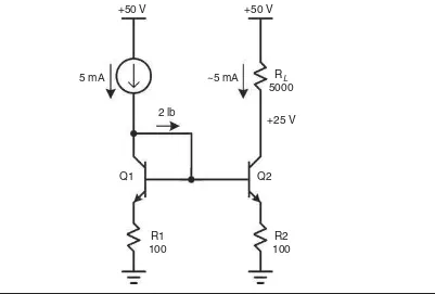
Current Mirror
Figure 2.9a depicts a very useful circuit called a current mirror. If a given amount of current is sourced into Q1, that same amount of current will be sunk by Q2, assuming that the emitter degeneration resistors R1 and R2 are equal, that the transistor Vbe drops are the same, and that losses through base currents can be ignored. The values of R1 and R2 will often be selected to drop about 100 mV to ensure decent matching in the face of unmatched transistor Vbe drops, but this is not critical.
FIGURE 2.9a Simple current mirror.
+50 V +50 V
+25 V 2 lb
Q2 Q1
5 mA ~5 mA RL
5000
R2 100 R1
If R1 and R2 are made different, a larger or smaller multiple if the input current can be made to flow in the collector of Q2. In practice, the base currents of Q1 and Q2 cause a small error in the output current with respect to the input current. In the example above, if transistor is 100, the base current Ib of each transistor will be 50 A, causing a total error of 100 A, or 2% in the output current.
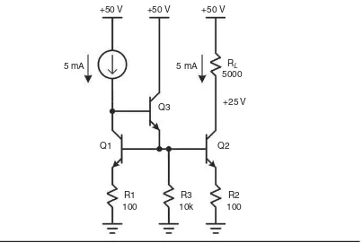
Figure 2.9b shows a variation of the current mirror that minimizes errors due to the finite current gain of the transistors. Here emitter follower Q3, often called a helper tran-sistor, provides current gain to minimize that error. Resistor R3 assures that a small minimum amount of current flows in Q3 even if the current gains of Q1 and Q2 are very high. Note that the input node of the current mirror now sits one Vbe higher above the supply rail than in Figure 2.9a.
Many other variations of current mirrors exist, such as the Wilson current mirror
shown in Figure 2.9c.The Wilson current mirror includes transistors Q1, Q2, and Q3.
Input current is applied to the base of Q3 and is largely balanced by current flowing in the collector of Q1. Input current that flows into the base of output transistor Q3 will turn Q3 on, with its emitter current flowing through Q2 and R2. Q1 and Q2 form a con-ventional current mirror. The emitter current of Q3 is mirrored and pulled from the source of input current by Q1.
Any difference between the current of Q1 and the input current is available to drive the base of Q3. If the input current exceeds the mirrored emitter current of Q3, the base voltage of Q3 will increase, causing the emitter current of Q3 to increase and self-correct the situation with feedback action. The equilibrium condition can be seen to be when the input current and the output current are the same, providing an overall 1:1 current mirror function.
Notice that in normal operation all three of the transistors operate at essentially the same current, namely the supplied input current. Ignoring the Early effect, all of the base currents will be the same if the betas are matched. Assume that each base current
+50 V +50 V +50 V
+25 V
Q2 Q1
Q3
5 mA 5 mA RL
5000
R1 100
R2 100 R3
10k
is Ib and that the collector current in Q1 is equal to I. It can be quickly seen that the input current must then be I Ib and that the emitter current of Q3 must be I 2Ib. It is then evident that the collector current of Q3, which is the output current, will be I Ib, which is the same as the input current. This illustrates the precision of the input-output rela-tionship when the transistors are matched.
Transistor Q3 acts much like a cascode, and this helps the Wilson current mirror to achieve high output impedance. Transistors Q1 and Q2 operate at a low collector volt-age, while output transistor Q3 will normally operate at a higher collector voltage. Thus, the Early effect will cause the base current of Q3 to be smaller, and this will result in a slightly higher voltage-dependent output current. This is reflected in the output resistance of the Wilson current mirror.
Current Sources
Current sources are used in many different ways in a power amplifier, and there are many different ways to make a current source. The distinguishing feature of a current source is that it is an element through which a current flows wherein that current is independent of the voltage across that element. The current source in the tail of the dif-ferential pair is a good example of its use.
Most current sources are based on the observation that if a known voltage is impressed across a resistor, a known current will flow. A simple current source is shown in Figure 2.10a. The voltage divider composed of R2 and R3 places 2.7 V at the base of Q1. After a Vbe drop of 0.7 V, about 2 V is impressed across emitter resistor R1. If R1 is a 400- resistor, 5 mA will flow in R1 and very nearly 5 mA will flow in the collector of Q1. The collector current of Q1 will be largely independent of the voltage at the collec-tor of Q1, so the circuit behaves as a decent current source. The load resistance RL is just shown for purposes of illustration. The output impedance of the current source itself (not including the shunting effect of RL) will be determined largely by the Early effect in FIGURE 2.9c Wilson current mirror.
+50 V +50 V
+25 V
lb
Q2 Q3
Q1
5 mA 5 mA
2 lb
RL 5000
R1 100
the same way as for the CE stage. The output impedance for this current source is found by SPICE simulation to be about 290 k .
In Figure 2.10b, R3 is replaced with a pair of silicon diodes. Here one diode drop is impressed across R1 to generate the desired current. The circuit employs 1N4148 diodes biased with the same 0.5 mA used in the voltage divider in the first example. Together FIGURE 2.10a Simple current source.
+50 V +50 V
+25 V
Q1 2N5551
0.5 mA ~5 mA RL
5000
R2 95k
R3 5.4k
R1 400 2.0 V 2.7 V
+50 V +50 V
+25 V
1N4148
1N4148
Q1 2N5551
0.5 mA ~5 mA RL
5000
R2 99k
R1 75 0.38 V 1.11 V
they drop only about 1.1 V, and about 0.38 V is impressed across the 75- resistor R1. The output impedance of this current source is approximately 300 k , about the same as the one above.
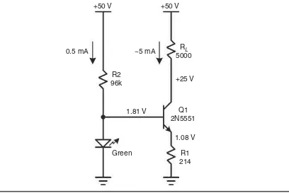
Turning to Figure 2.10c, R3 is replaced instead with a Green LED, providing a
convenient voltage reference of about 1.8 V, putting about 1.1 V across R1. Once again, 0.5 mA is used to bias the LED. The output impedance of this current source is about 750 k . It is higher than in the design of Figure 2.10b because there is effectively more emitter degeneration for Q1 with the larger value of R1.
R3 is replaced with a 6.2-V Zener diode in Figure 2.10d. This puts about 5.5 V across R1. The output impedance of this current source is about 2 M , quite a bit higher than the earlier arrangements due to the larger emitter degeneration for Q1. The price paid here is that the base of the transistor is fully 6.2 V above the supply rail, reducing head-room in some applications.
In Figure 2.10e, a current mirror fed from a known supply voltage is used to imple-ment a current source. Here a 1:1 current mirror is used and 5 mA is supplied from the known power rail. The output impedance of this current source is about 230 k . Only 0.25 V is dropped across R1 (corresponding to 10:1 emitter degeneration), and the base is only 1 V above the rail.
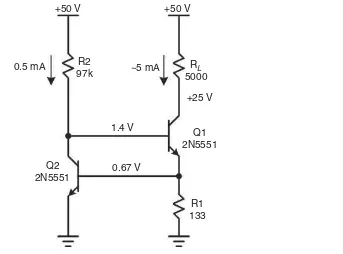
Figure 2.10fillustrates a clever two-transistor feedback circuit that is used to force one Vbe of voltage drop across R1. It does so by using transistor Q2 to effectively regu-late the current of Q1. If the current of Q1 is too large, Q2 will be turned on harder and pull down on the base of Q1, adjusting its current downward appropriately. As in Fig-ure 2.10a through 2.10d, a 0.5-mA current is supplied to bias the current source. This current flows through Q2. The output impedance of this current source is an impressive 3 M . This circuit achieves higher output impedance than the Zener-based version and yet only requires the base of Q1 to be 1.4 V above the power rail. This circuit can also be used to place an overcurrent limit on a CE transistor stage implemented with Q1.
+50 V +50 V
+25 V
Q1 2N5551
0.5 mA ~5 mA RL
5000
R2 96k
R1 214 Green
1.08 V 1.81 V
This circuit will work satisfactorily even if less than 0.5 mA (one-tenth of the output current) is supplied as bias for Q2, but then the output impedance will fall to a lower value and the “quality” of the current source will suffer somewhat. This happens because at lower collector current, Q2 has less transconductance and its feedback con-trol of the current variations in Q1 as a result of the Early effect is less strong. If the bias current is reduced to 0.1 mA, for example, the output impedance falls to about 1 M .
+50 V +50 V
6.2 V
Q1 2N5551
0.5 mA ~5 mA RL
5000
+25 V R2
88k
R1 1.1k 5.5 V 6.2 V
FIGURE 2.10d Current source using Zener diode.
+50 V +50 V
Q1 2N5551 Q2
2N5551
5 mA ~5 mA RL
5000
+25 V R2
9.8k
R1 50 R3
50
0.25 V 0.98 V
V
beMultiplier
Figure 2.11 shows what is called a Vbe multiplier. This circuit is used when a voltage drop equal to some multiple of Vbe drops is needed. This circuit is most often used as the bias spreader for power amplifier output stages, partly because its voltage is conveniently adjustable.
FIGURE 2.10f Feedback current source.
+50 V +50 V
Q1 2N5551
Q2 2N5551
0.5 mA ~5 mA RL
5000
+25 V R2
97k
R1 133 1.4 V
0.67 V
FIGURE 2.11 Vbe multiplier.
+50 V
Q1 2N5551
10 mA
~3.0 V
R1 2100
R2 700
0.75 V
9 mA
In the circuit shown, the Vbe of Q1 is multiplied by a factor of approximately 4. Notice that the voltage divider formed by R1 and R2 places about one-fourth of the col-lector voltage at the base of Q1. Thus, in equilibrium, when the voltage at the colcol-lector is at four Vbe, one Vbe will be at the base, just enough to turn on Q1 by the amount neces-sary to carry the current supplied. This is simply a shunt feedback circuit. In this arrangement, about 1 mA flows through the resistive divider while about 9 mA flows through Q1.
When the Vbe multiplier is used as a bias spreader, R2 will be made adjustable with a trim pot. As R2 is made smaller the amount of bias voltage is increased. Notice that if for some reason R2 fails open, the voltage across the Vbe multiplier falls to about one Vbe, failing in the safe direction.
In practice the Vbe multiplication ratio will be a bit greater than 4 due to the base current required by Q1 as a result of its finite current gain. The extra drop caused across R1 by the base current will slightly increase the collector voltage at equilibrium, making the apparent multiplier factor slightly larger than 4.
The impedance of the Vbe multiplier is about 4 re for Q1. At 9 mA, re is 2.9 , so ideally the impedance of the multiplier would be about 11.6 . In practice, SPICE simu-lation shows it to be about 25 . This larger value is mainly a result of the finite current gain of Q1.
The impedance of the Vbe multiplier rises at high frequencies. This is a result of the fact that the impedance is established by a negative feedback process. The amount of feedback decreases at high frequencies and the impedance-reducing effect is lessened. The impedance of the Vbe multiplier in Figure 2.11 is up by 3 dB at about 2.3 MHz and doubles for every octave increase in frequency from there. It is thus inductive. For this reason, the Vbe multiplier is often shunted by a capacitor of 0.1 to 10 F. A shunt capacitance of as little as 0.1 F eliminates the increase in imped-ance at high frequencies.
2.3 Amplifier
Design
Analysis
Here we apply the understanding of transistors and circuit building blocks to analyze the basic power amplifier. Having accomplished this, we will be well armed to explore, evolve, and analyze the amplifier design steps that will be taken to achieve high perfor-mance in the next chapter.
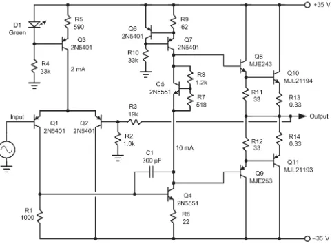
Figure 2.12 is a schematic of a basic 50-W power amplifier that includes the three stages that appear in most solid-state power amplifiers.
–Q3
–Q11
The design also includes a bias spreader implemented with Q5 connected as a Vbe
multiplier. Some details like coupling capacitors, input networks, and output networks have been left out for simplicity.
Basic Operation
This simple design is a more detailed version of the basic amplifier design illustrated in Figure 1.5. As shown, it is a DC-coupled design, so that even DC changes at the input will be amplified and presented at the output.
Input Stage
The input signal is applied to the input differential pair at the base of Q1. A fraction of the output signal is coupled via the negative feedback path to the other differential input at the base of Q2. Transistor Q3 implements a 2-mA current source that provides tail current to the differential pair. This input arrangement is often called a Long-Tailed Pair(LTP).
Feedback resistors R2 and R3 implement a voltage divider that feeds back 1/20 of the output signal to the input stage. The forward path gain of the amplifier in the absence of negative feedback is called the open-loop gain (Aol). If the open-loop gain is large, then the error signal across the bases of Q1 and Q2 need only be very small to produce the desired output. If the signals at the bases of Q1 and Q2 are nearly equal, then the output of the amplifier must be 20 times that of the input, resulting in a closed-loop gain (Acl) of 20. This is just a very simplified explanation of the negative feedback process.
The approximate low-frequency gain of the input stage is the ratio of the net col-lector load resistance divided by the total emitter-to-emitter resistance RLTP (which includes the intrinsic emitter resistance re of Q1 and Q2). With each transistor biased at 1 mA, the intrinsic emitter resistance re is about 26 each, so the total emitter-to-emitter resistance is 52 . If we assume that the of the following VAS transistor Q4 is infinity, the net IPS collector load resistance is just that of R1. The DC gain of the IPS is then 1000/52 19. In practice the finite of Q4 reduces this to about 13.7 if we assume that the of Q4 is 100.
IPS gain 13.7
The amplifier at low frequencies is illustrated in Figure 2.13 where the input stage is shown as a block of transconductance with gm 1/52 0.019 S. The R1 load of 714 on the IPS is just the parallel combination of R1 and the estimated input imped-ance of the VAS.
The VAS
The VAS is formed by common-emitter transistor Q4 loaded by the 10-mA current source formed by Q6 and Q7. Recall from the discussion of current sources above that Q6 forces one Vbe (here about 620 mV) across 62- resistor R9; this produces the desired current flow.
Emitter degeneration has been applied to Q4 in the form of R6. At 10 mA, re of Q4 is about 2.6 . The 22- resistance of R6 therefore increases the total effective emitter circuit resistance to about 25 , or by a factor of nearly 10. This corresponds to 10:1 emitter degeneration. The emitter degeneration makes the VAS stage more linear in its operation.
If the of Q4 is assumed to be 100, the input impedance of the VAS will be about 100 25 2500 . This impedance is in parallel with R1, making the actual load on the first stage approximately 714 . The voltage gain of the input stage is therefore close to 13.7. The loading of Q4 thus plays a substantial role in determining the first-stage gain. It would play a far greater role if Q4 were not degenerated by R6. In that case the impedance seen looking into the base of Q4 would be only about 260 ( 100 times re 2.6 ).