i
SISTEM KENDALI BISING AKTIF UNTUK FAN KOMPUTER
MENGGUNAKAN ALGORITMA ANFIS
Yudhistira Utomo / 0322126
Jurusan Teknik Elektro, Fakultas Teknik, Universitas Kristen Maranatha,
Jln. Prof. Drg. Surya Sumantri 65, Bandung 40164, Indonesia
Email : [email protected]
ABSTRAK
Konsumsi daya dari komputer saat ini semakin besar. Hal tersebut menghasilkan
panas yang cukup besar, akibatnya dibutuhkan banyak fan pendingin. Penggunaan
banyaknya fan pendingin tersebut menghasilkan bising yang tidak dikehendaki. Oleh
karena itu timbul motivasi untuk meredam bising tersebut.
Untuk meredam bising tersebut maka digunakan sistem kendali bising secara aktif.
Bising merupakan sinyal yang memiliki karakteristik yang non linear. Untuk
menggambarkan karakteristik bising tersebut diperlukan suatu model matematis, akan
tetapi penentuan model matematis tesebut adalah sulit. Digunakan metoda Logika Fuzzy
dengan algoritma Adaptive Neuro Fuzzy Inference System (ANFIS) untuk mempelajari
karakteristik yang non linear tersebut.
Dalam merealisasi suatu ANFIS dibutuhkan sejumlah pasangan data latih. ANFIS
akan melakukan penalaan pada fungsi keanggotaan tersebut dengan menggunakan aturan
pembelajaran hibrida dari metoda
gradient descent
dan
least squares estimation
berdasarkan data latih yang diberikan.
Hasil dari simulasi dari sistem kendali bising aktif ini adalah sinyal bising yang
mampu diredam dengan tingkat peredaman 1,0669 kali. Angka ini diperoleh dari
perbandingan variansi amplituda sinyal bising setelah melewati duct dengan variansi
amplituda sinyal residu.
Pada implementasi perangkat keras, sistem ini gagal meredam sinyal bising yang
dihasilkan oleh fan komputer. Penyebab kegagalannya adalah amplituda sinyal bising
terlalu kecil, sehingga sistem gagal mengestimasi model dari duct.
ii
USING ANFIS ALGORITHM
Yudhistira Utomo / 0322126
Department of Electric Engineering, Faculty of Technique, Maranatha Christian
University, Jln. Prof. Drg. Surya Sumantri 65, Bandung 40164, Indonesia
Email : [email protected]
ABSTRACT
High energy consumption of personal computer yields high temperature. In order
to reduce high temperature, some cooling fans required. The employs of cooling fans,
however, produce noise which need to be reduced. Thus, the major effort of this final
project is reduce acoustic noise of computer fan.
In this final project an active noise controller is used to reduce acoustic noise. Due
to the non linear characteristic of the plant, the generation of its mathematical model is
too dificult to be implemented. Then, fuzzy logic method with ANFIS algorithm is used
as the solution.
The realization of ANFIS required some of data pairs. ANFIS will adjust the
membership function using training rule of hybrid from gradient descent and least
squares estimation methods, which are based on the given training data.
Simulation shows that, the active noise controller system is able to cancel noise
with the level cancellation of 1.0669. The cancellation level is taken as the ratio of
amplitude of the noise signal and amplitude of error signal.
Hardware implementation showsthat, active noise controller system has failed to
canceling noise signal. The reason is that the amplitude of the noise signal too small, so
that the system fail to estimate the mathematical model of the duct.
iii
KATA PENGANTAR
Puji syukur dan terima kasih diucapkan kepada Tuhan Yang Maha Esa karena atas berkat dan rahmat-Nya, tugas akhir ini dapat diselesaikan dengan baik. Tugas akhir yang berjudul “Sistem Kendali Bising Aktif Untuk Fan Komputer Menggunakan Algoritma ANFIS” ini disusun untuk memperoleh gelar Strata 1 (S1) Fakultas Teknik Jurusan Teknik Elektro di Universitas Kristen Maranatha.
Dalam penyelesaian tugas akhir ini, penulis telah banyak mendapatkan bantuan dari berbagai pihak. Untuk itu, dalam kesempatan ini penulis mengucapkan terima kasih yang sebesar-besarnya kepada :
1. Papa dan Ibu tercinta yang selalu memberikan dukungan moral maupun materi.
2. Bapak Hendra Tjahyadi, Ph.D. selaku pembimbing tugas akhir yang menyumbangkan pengetahuan, memberikan masukan berupa ide-ide, kritik dan saran, dan membimbing penyusun hingga tugas akhir ini dapat diselesaikan.
3. Bapak Riko Arlando Saragih, ST., MT., Ibu Dr. E. Merry Sartika, dan Ibu Novie T. Pasaribu, ST., MT., selaku dosen penguji yang telah memberikan banyak masukan dalam seminar tugas akhir.
4. Bapak Dr. Daniel Setiadikarunia, selaku Ketua Jurusan Teknik Elektro Universitas Kristen Maranatha.
5. Ibu Ir. Anita Supartono M.Sc., selaku Koordinator Tugas Akhir Jurusan Teknik Elektro Universitas Kristen Maranatha.
6. Bapak Ir. Kok King Lok, selaku dosen wali penulis yang telah memotivasi dan membimbing penulis selama menempuh masa perkuliahan.
7. Bapak Muliady, ST., MT. yang telah memberikan bahan referensi bagi tugas akhir penulis
iv
perpustakaan, dan seluruh karyawan Universitas Kristen Maranatha, atas bantuannya selama masa kuliah penulis.
10.Galih, Nurjani, Yogi, Ivans, Windu, Agus, Nehemia, Daniel, David, Hosken, Martin, Tysan, Ate, Angki, Lina, Inggar, Jongguran, Kurniawan, Willy, Rizky H, Vania, dan rekan-rekan angkatan 2000, 2001, 2002, 2003, 2004, 2005, dan 2006 jurusan teknik elektro lainnya, yang namanya tidak cukup untuk dituliskan satu persatu di sini, atas dukungan, semangat, doa dan bantuannya kepada penulis.
11.Rekan – rekan penulis di 3POD photography, Rubinhut, Yohanes, Leska, Made, dan Angga atas dukungan, semangat, doa dan bantuannya kepada penulis.
12.Bowo, Swarie, Riqa, Patriotika, Mila, Adam, Raymon, Fani, Andi, Agung, Dendi, dan rekan – rekan alumni SMA Negeri 3 Bandung lainnya.
13.R. Suci Indra Purnama yang selalu memberikan dukungan moral dan semangat kepada penulis
14.Serta semua pihak yang turut membantu penulis yang namanya tidak dapat penulis sebutkan satu persatu di sini.
Penulis menyadari bahwa tugas akhir ini masih jauh dari sempurna. Untuk itu, saran dan kritik yang bersifat membangun selalu dinantikan guna evaluasi sekaligus perbaikan di masa yang akan datang.
Penulis juga meminta maaf apabila terdapat kesalahan atau hal-hal yang tidak berkenan dalam penulisan laporan tugas akhir maupun selama pengerjaan tugas akhir.
Akhir kata, penulis berharap agar laporan tugas akhir ini dapat bermanfaat bagi pihak-pihak yang membutuhkan.
Bandung, September 2008
v
DAFTAR ISI
Abstrak ... i
Abstract ... ii
Kata Pengantar ... iii
Daftar Isi ... v
Daftar Gambar ... vii
Daftar Tabel ... x
BAB I Pendahuluan 1.1 Latar Belakang ... 1
1.2 Identifikasi Masalah ... 1
1.3 Perumusan Masalah ... 2
1.4 Tujuan ... 2
1.5 Pembatasan Masalah ... 2
1.6 Spesifikasi Alat ... 3
1.7 Sistematika Penulisan ... 3
BAB II Dasar Teori 2.1 Konsep Umum ... 5
2.2 Teori Akustik ... 7
2.2.1 Perambatan Gelombang ... 7
2.2.2 Peredam Pasif ... 8
2.2.3 Peredam Aktif ... 8
2.3 Sistem Kendali Bising Aktif ... 9
2.3.1 Sistem Kendali Bising Aktif Umpan Balik ... 9
2.3.1 Sistem Kendali Bising Aktif Umpan Maju ... 11
2.4 Aplikasi – Aplikasi Sistem Kendali Bising Aktif ... 13
2.4.1 Kendali Bising Aktif Akustik Udara ... 14
2.5 Konsep Peredam Bising Adaptif ... 14
vi
2.7.1 Fuzzy Inference System (FIS) ... 16
2.7.2 Jaringan Adaptif ... 19
2.7.3 Algoritma Backpropagation untuk Jaringan Umpan Maju ... 21
2.7.4 Aturan Pembelajaran Hibrid ... 23
2.7.4.1 Aturan Pembelajaran Hibrid Off-Line ... 24
2.7.4.2 Aturan Pembelajaran Hibrid On-Line ... 26
2.7.5 Adaptive Network-Based Fuzzy Inference System (ANFIS) . 27 2.8 Penghitungan Matematis Pembuktian Peredaman Sinyal Bising …… 30
2.9 Program MATLAB ... 30
2.9.1 Beberapa Bagian dari Window Matlab ... 31
BAB III Perancangan 3.1 Pengambilan Data Sinyal Sumber Bising ... 34
3.2 Analisa Frekuensi Sinyal Sumber Bising ... 36
3.3 Perancangan ANFIS ... 36
3.3.1 Pengumpulan Data Latih ... 36
3.3.2 Penentuan Jumlah dan Bentuk Fungsi Keanggotaan ... 37
3.3.3 Pelatihan ANFIS ... 38
3.4 Simulasi Sistem Kendali Bising Aktif Menggunakan ANFIS ... 38
3.5 Perancangan Sistem Kendali Bising Aktif Menggunakan ANFIS ... 41
3.5.1 Perangkat Lunak ... 41
3.5.2 Perangkat Keras ... 42
3.5.2.1 Mikrofon dan Speaker... 43
3.5.2.2 Komputer ... 43
3.5.2.3 Duct ... 43
3.5.3 Konfogurasi Perangkat Keras ... 45
BAB IV Analisa Hasil Percobaan 4.1 Analisa Frekuensi Sinyal Bising ... 47
4.2 Analisa Hasil Pelatihan ANFIS ... 48
4.3 Analisa Hasil Simulasi ... 49
vii
4.3.2 Simulasi Kedua ... 53 4.3.3 Simulasi Ketiga ... 57 4.3.4 Simulasi Keempat ... 62 4.4 Analisa Hasil Implementasi Perangkat Lunak Pada Perangkat Keras . 67 BAB V Kesimpulan dan Saran
5.1 Kesimpulan ... 78 5.2 Saran ... 79 DAFTAR PUSTAKA... 80 LAMPIRAN A HASIL PELATIHAN ANFIS
viii
Gambar 2.1 Konsep Dasar dari Sistem Kendali Bising Aktif ... 6 Gambar 2.2 Sistem kendali peredam bising umpan balik pada duct .... 10 Gambar 2.3 Sistem umpan balik dengan estimator dan tanpa estimator 10 Gambar 2.4 Sistem kendali peredam bising umpan maju pada duct .... 11 Gambar 2.5 Konsep peredam bising adaptif ... 14 Gambar 2.6 Blok Diagram Sistem Kendali Bising Aktif
Menggunakan ANFIS dengan Umpan Maju ... 15 Gambar 2.7 Aturan fuzzy if-then dan penarikan kesimpulan yang sering
digunakan ... 18 Gambar 2.7 Fuzzy inference system ... 19 Gambar 2.8 Jaringan adaptif ... 19 Gambar 2.9 (a) Model fuzzy Sugeno tingkat pertama dengan dua masukan 27 Gambar 2.9 (b) Arsitektur ANFIS ... 27 Gambar 2.10 Arsitektur ANFIS model fuzzy Sugeno orde pertama
dengan dua masukan yang memiliki sembilan aturan; .... 30 Gambar 2.10 (b) Ruang masukan dua dimensi yang dibagi menjadi
sembilan daerah fuzzy ... 30 Gambar 2.11 Tampilan Program MATLAB ... 33 Gambar 3.1 Diagram blok Simulink, perubahan data sumber
bising menjadi bentuk matrik. ... 35 Gambar 3.2 Diagram blok Simulink pengambilan data pelatihan
ix
Gambar 3.10 Realisasi Duct ... 44 Gambar 3.11 Konfigurasi Perangkat Keras ... 45 Gambar 3.12 Gambar Realisasi Perangkat Keras Sistem Kendali Bising
Aktif Pada Fan Komputer Menggunakan Algoritma
ANFIS ... 46 Gambar 4.1 Analisa Frekuensi Sinyal Bising ... 47 Gambar 4.2 Diagram Blok Simulasi Pertama Sistem Kendali Bising
Aktif ... 49 Gambar 4.3 Perbandingan Sinyal Bising Sebelum Melewati duct
dan Setelah Melewati Duct Pada Simulasi Pertama ... 50 Gambar 4.4 Sinyal Anti Bising Pada Simulasi Pertama ... 51 Gambar 4.5 Perbandingan Sinyal Bising Setelah Melewati duct
Dengan Sinyal Residu Pada Simulasi Pertama ... 52 Gambar 4.6 Diagram Blok Simulasi Kedua Sistem Kendali Bising
Aktif ... 54 Gambar 4.7 Perbandingan Sinyal Bising Sebelum Melewati duct
dan Setelah Melewati Duct Pada Simulasi Kedua ... 55 Gambar 4.8 Sinyal Anti Bising Pada Simulasi Kedua ... 55 Gambar 4.9 Perbandingan Sinyal Bising Setelah Melewati duct
Dengan Sinyal Residu Pada Simulasi Kedua ... 56 Gambar 4.10 Diagram Blok Simulasi Ketiga Sistem Kendali Bising
Aktif 55
Gambar 4.11 Perbandingan Sinyal Bising Sebelum Melewati duct
dan Setelah Melewati Duct Pada Simulasi Ketiga ... 59 Gambar 4.12 Sinyal Anti Bising Pada Simulasi Ketiga ... 60 Gambar 4.13 Perbandingan Sinyal Bising Setelah Melewati duct
Dengan Sinyal Residu Pada Simulasi Ketiga ... 61 Gambar 4.14 Diagram Blok Simulasi Ketiga Sistem Kendali Bising
Aktif 60
Gambar 4.15 Perbandingan Sinyal Bising Sebelum Melewati duct
x
Dengan Sinyal Residu Pada Simulasi Keempat ... 66 Gambar 4.18 Diagram Blok Perangkat Lunak Sistem Kendali Bising
Aktif ... 68 Gambar 4.19 Perbandingan Sinyal Bising Sebelum Melewati duct
dan Setelah Melewati Duct Pada Percobaan Perangkat
Keras ... 69 Gambar 4.20 Sinyal Anti Bising Pada Percobaan Perangkat Keras ... 70 Gambar 4.21 Perbandingan Sinyal Bising Setelah Melewati duct
Dengan Sinyal Residu Pada Percobaan Perangkat Keras . 71 Gambar 4.22 Perbandingan Sinyal Bising Sebelum Melewati duct
dan Setelah Melewati Duct Pada Percobaan Kedua
Perangkat Keras ... 73 Gambar 4.23 Sinyal Anti Bising Pada Percobaan Kedua Perangkat
Keras ... 74 Gambar 4.24 Perbandingan Sinyal Bising Setelah Melewati duct
Dengan Sinyal Residu Pada Percobaan Kedua
xi
DAFTAR TABEL
Tabel 4.1 Variansi Amplituda Sinyal Pada Simulasi Pertama ... 53
Tabel 4.2 Variansi Amplituda Sinyal Pada Simulasi Kedua ... 57
Tabel 4.3 Variansi Amplituda Sinyal Pada Simulasi Ketiga ... 62
Tabel 4.4 Variansi Amplituda Sinyal Pada Simulasi Keempat ... 67
Tabel 4.5 Variansi Amplituda Sinyal Pada Percobaan Perangkat Keras ... 72
LAMPIRAN A
AC ’97 and HD Audio
SoundMAX Codec
AD1986A
Rev.0
Information furnished by Analog Devices is believed to be accurate and reliable. However, no responsibility is assumed by Analog Devices for its use, nor for any infringements of patents or other rights of third parties that may result from its use. Specifications subject to change without notice. No license is granted by implication or otherwise under any patent or patent rights of Analog Devices. Trademarks and registered trademarks are the property of their respective owners.
One Technology Way, P.O. Box 9106, Norwood, MA 02062-9106, U.S.A. Tel: 781.329.4700 www.analog.com
Fax: 781.461.3113 © 2005 Analog Devices, Inc. All rights reserved.
FEATURES
Supports both AC ’97 and HD audio interfaces 6 DAC channels for 5.1 surround
S/PDIF output
Integrated headphone amplifiers Variable rate audio
Double rate audio (Fs = 96 kHz)
Greater than 90 dB dynamic range 20-bit resolution on all DACs 20-bit resolution on all ADCs Line-level mono phone input High quality differential CD input Selectable MIC input with preamp AUX and line-in stereo inputs
External amplifier power down (EAPD) Power management modes
Jack sensing and device identification 48-lead LQFP package
ENHANCED FEATURES
Integrated parametric speaker equalizer Stereo microphone with up to 30 dB gain boost Integrated PLL for system clocking
Variable sample rate: 7 kHz to 96 kHz 7 kHz to 48 kHz in 1 Hz increments 96 kHz for double rate audio
Jack sense with autotopology switching Jack presence detection on up to 8 jacks
Three software-controlled microphone bias signals Software-enabled outputs for jack sharing
Auto-down mix and channel spreading
Microphone-to-mono output for speakerphone Stereo microphone pass-through to mixer Built-in microphone/center/LFE/line-in sharing Built-in SURROUND/LINE_IN sharing
Center/LFE swapping supporting all vendor speakers Microphone left/right swapping
Rev. 0 | Page 3 of 56
NOTES
REDUCED SUPPORT COMPONENTS
The AD1986A includes many improvements that reduce external support components for particular applications. • Multiple Microphone Sourcing: The MIC_1/2, LINE_IN
and C/LFE pins can all be selected as sources for microphone input (boost amplifier).
• Multiple VREF_OUT Pins: Each microphone-capable pin group (MIC_1/2, LINE_IN and C/LFE) has separate, software controllable VREF_OUT pins, reducing the need for external biasing components.
• Internal Microphone Mixing: Any combination of the MIC_1/2, LINE_IN and C/LFE pins can be summed to produce the microphone input. This removes the need for external mixing components in applications that externally mix microphone sources.
• Advanced Jack Presence Detection: Using two codec pins, eight resistors and isolated switch jacks, the AD1986A can detect jack insertion on eight separate jacks.
• Internal Microphone/Line In/C/LFE Sharing: On systems that share the microphone with the C/LFE jack no external components are required. The microphone selector can select the LINE_IN pins when the microphone and line input devices are swapped.
• Internal Line In/Microphone/Surround Sharing: On systems that share the line in with the surround jack no external components are required.
AD1986A
Rev. 0 | Page 5 of 56
SPECIFICATIONS
Test conditions, unless otherwise noted.
Table 1.
Parameter Typ Unit
Temperature 25 °C
Digital Supply (DVDD) 3.3 ± 10% V
Analog Supply (AVDD) 5.0 ± 10% V
Sample Rate (FS) 48 kHz
Input Signal 1.0 kHz
Analog Output Pass Band 20 Hz–20 kHz
VIH 2.0 V
VIL 0.8 V
VIH 2.4 V
VIL 0.6 V
DAC Test Conditions
Calibrated
Output −3 dB Relative to Full Scale
10 kΩ Output Load: Line (Surround), Mono 32 Ω Output Load: Headphone
2 kΩ Output Load: Center, LFE
ADC Test Conditions
Calibrated 0 dB PGA Gain
Input −3.0 dB Relative to Full Scale
Table 2. Analog Input
Input Voltage Min Typ Max Unit
MIC_1/2, LINE_IN, CD, AUX, PHONE_IN (No Preamp) 1 Vrms1
C/LFE and SURROUND (When Used as Inputs) 2.83 V p-p
MIC_1/2, LINE_IN, C/LFE With 30 dB Preamp 0.032 Vrms
0.089 V p-p
MIC_1/2, LINE_IN, C/LFE With 20 dB Preamp 0.1 Vrms
0.283 V p-p
MIC_1/2, LINE_IN, C/LFE With 10 dB Preamp 0.316 Vrms
0.894 V p-p
Input Impedance2 20 kΩ
Input Capacitance2 5 7.5 pF
1 RMS values assume sine wave input. 2 Guaranteed by design, not production tested.
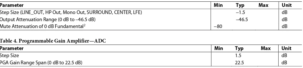
Table 3. Master Volume
Parameter Min Typ Max Unit
Step Size (LINE_OUT, HP Out, Mono Out, SURROUND, CENTER, LFE) −1.5 dB
Output Attenuation Range (0 dB to –46.5 dB) −46.5 dB
Mute Attenuation of 0 dB Fundamental2 −80 dB
Table 4. Programmable Gain Amplifier—ADC
Parameter Min Typ Max Unit
Step Size 1.5 dB
Rev. 0 | Page 6 of 56
Table 5. Analog Mixer—Input Gain/Amplifiers/Attenuators
Parameter Min Typ Max Unit
Signal-to-Noise Ratio (SNR)
CD to LINE_OUT 90 dB
LINE, AUX, PHONE to LINE_OUT1 88 dB
MIC_1 or MIC_2 to LINE_OUT1 80 dB
Step Size: All Mixer Inputs (Except PC Beep) −1.5 dB
Step Size: PC Beep −3.0 dB
Input Gain/Attenuation Range: All Mixer Inputs (+12 dB to −34.5 dB) −46.5 dB
1 Guaranteed by design, not production tested.
Table 6. Digital Decimation and Interpolation Filters1
Parameter Min Typ Max Unit
Pass Band 0 0.4 × FS Hz
Pass-Band Ripple ±0.09 dB
Transition Band 0.4 × FS 0.6 × FS Hz
Stop Band 0.6 × FS ∞ Hz
Stop-Band Rejection −74 dB
Group Delay 16/FS S
Group Delay Variation Over Pass Band 0 µs
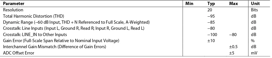
Table 7. Analog-to-Digital Converters
Parameter Min Typ Max Unit
Resolution 20 Bits
Total Harmonic Distortion (THD) −95 dB
Dynamic Range (−60 dB Input, THD + N Referenced to Full Scale, A-Weighted) −85 dB Crosstalk: Line Inputs (Input L, Ground R, Read R; Input R, Ground L, Read L) −80 dB
Crosstalk: LINE_IN to Other Inputs −100 −80 dB
Gain Error (Full-Scale Span Relative to Nominal Input Voltage) ±10 %
Interchannel Gain Mismatch (Difference of Gain Errors) ±0.5 dB
AD1986A
Rev. 0 | Page 7 of 56
Table 8. Digital-to-Analog Converters
Parameter Min Typ Max Unit
Resolution 20/24 Bits
Total Harmonic Distortion (LINE_OUT Drive) −92 dB
Total Harmonic Distortion (HP_OUT) −75 dB
Dynamic Range (−60 dB Input, THD + N Referenced to Full-Scale, A-Weighted) 91 dB Gain Error (Full-Scale Span Relative to Nominal Input Voltage) ±10 %
Interchannel Gain Mismatch (Difference of Gain Errors) ±0.7 dB
DAC Crosstalk1 (Input L, Zero R, Read R_OUT; Input R, Zero L, Read L_OUT) −80 dB
1 Guaranteed by design, not production tested.
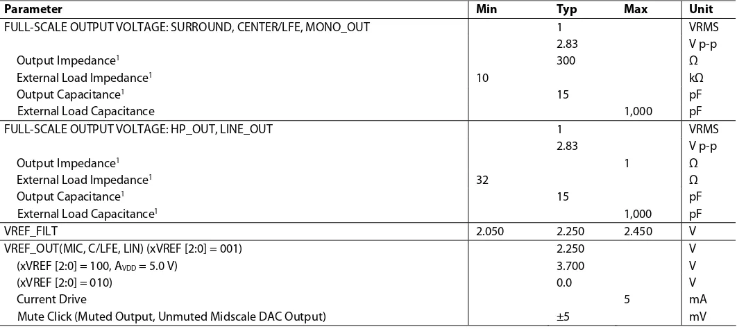
Table 9. Analog Output
Parameter Min Typ Max Unit
FULL-SCALE OUTPUT VOLTAGE: SURROUND, CENTER/LFE, MONO_OUT 1 VRMS
2.83 V p-p
Output Impedance1 300 Ω
External Load Impedance1 10 kΩ
Output Capacitance1 15 pF
External Load Capacitance 1,000 pF
FULL-SCALE OUTPUT VOLTAGE: HP_OUT, LINE_OUT 1 VRMS
2.83 V p-p
Output Impedance1 1 Ω
External Load Impedance1 32 Ω
Output Capacitance1 15 pF
External Load Capacitance1 1,000 pF
VREF_FILT 2.050 2.250 2.450 V
VREF_OUT(MIC, C/LFE, LIN) (xVREF [2:0] = 001) 2.250 V
(xVREF [2:0] = 100, AVDD = 5.0 V) 3.700 V
(xVREF [2:0] = 010) 0.0 V
Current Drive 5 mA
Mute Click (Muted Output, Unmuted Midscale DAC Output) ±5 mV
1 Guaranteed by design, not production tested.
Table 10. Static Digital Specifications—AC ’97
Parameter Min Typ Max Unit
High Level Input Voltage (VIH), Digital Inputs 0.65 × DVDD V
Low Level Input Voltage (VIL) 0.35 × DVDD V
High Level Output Voltage (VOH), IOH = 2 mA 0.90 × DVDD V
Low Level Output Voltage (VOL), IOL = 2 mA 0.10 × DVDD V
Input Leakage Current −10 10 µA
Output Leakage Current −10 10 µA
Rev. 0 | Page 8 of 56
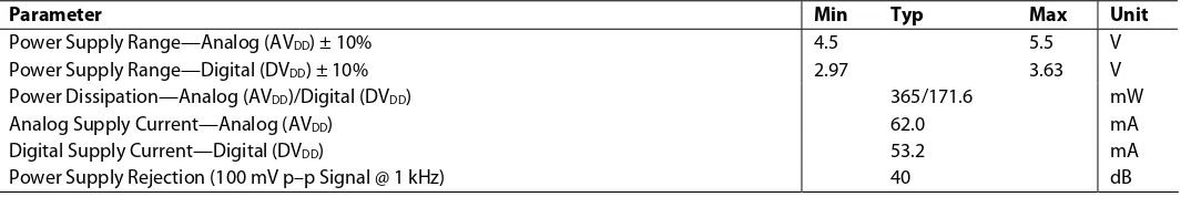
Table 11. Power Supply (Quiescent State)
Parameter Min Typ Max Unit
Power Supply Range—Analog (AVDD) ± 10% 4.5 5.5 V
Power Supply Range—Digital (DVDD) ± 10% 2.97 3.63 V
Power Dissipation—Analog (AVDD)/Digital (DVDD) 365/171.6 mW
Analog Supply Current—Analog (AVDD) 62.0 mA
Digital Supply Current—Digital (DVDD) 53.2 mA
Power Supply Rejection (100 mV p–p Signal @ 1 kHz) 40 dB
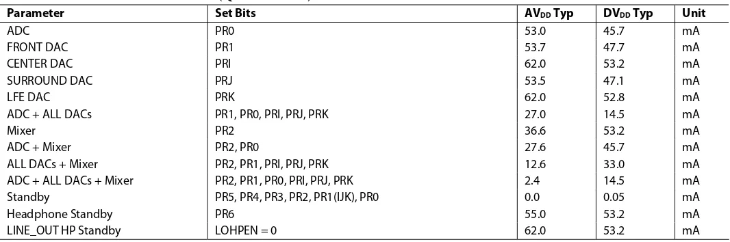
Table 12. Power-Down States—AC ’97 (Quiescent State)
Parameter Set Bits AVDD Typ DVDD Typ Unit
ADC PR0 53.0 45.7 mA
FRONT DAC PR1 53.7 47.7 mA
CENTER DAC PRI 62.0 53.2 mA
SURROUND DAC PRJ 53.5 47.1 mA
LFE DAC PRK 62.0 52.8 mA
ADC + ALL DACs PR1, PR0, PRI, PRJ, PRK 27.0 14.5 mA
Mixer PR2 36.6 53.2 mA
ADC + Mixer PR2, PR0 27.6 45.7 mA
ALL DACs + Mixer PR2, PR1, PRI, PRJ, PRK 12.6 33.0 mA
ADC + ALL DACs + Mixer PR2, PR1, PR0, PRI, PRJ, PRK 2.4 14.5 mA
Standby PR5, PR4, PR3, PR2, PR1(IJK), PR0 0.0 0.05 mA
Headphone Standby PR6 55.0 53.2 mA
LINE_OUT HP Standby LOHPEN = 0 62.0 53.2 mA
Table 13. Clock Specifications
Parameter Min Typ Max Unit
Input Clock Frequency (Reference Clock Mode) 14.31818
48.000
MHz MHz
Recommended Clock Duty Cycle 40 50 60 %
AD1986A
Rev. 0 | Page 9 of 56
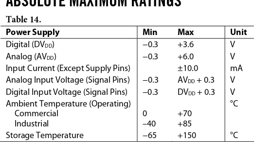
ABSOLUTE MAXIMUM RATINGS
Table 14.
Power Supply Min Max Unit
Digital (DVDD) −0.3 +3.6 V
Analog (AVDD) −0.3 +6.0 V
Input Current (Except Supply Pins) ±10.0 mA Analog Input Voltage (Signal Pins) −0.3 AVDD + 0.3 V
Digital Input Voltage (Signal Pins) −0.3 DVDD + 0.3 V
Ambient Temperature (Operating) Commercial Industrial 0 –40 +70 +85 °C
Storage Temperature −65 +150 °C
Stresses greater than those listed under Absolute Maximum Ratings can cause permanent damage to the device. This is a stress rating only, functional operation of the device at these or any other conditions above those indicated in the operational section of this specification is not implied. Exposure to absolute maximum rating conditions for extended periods can affect device reliability.
ENVIRONMENTAL CONDITIONS
Ambient Temperature Rating TAMB = TCASE − (PD × θCA)
TCASE = case temperature in °C
PD = power dissipation in W
θCA = thermal resistance (case-to-ambient)
θJA = thermal resistance (junction-to-ambient)
θJC = thermal resistance (junction-to-case)
Table 15. Thermal Resistance
Package θJA θJC θCA
LQFP 48°C/W 17°C/W 31°C/W
LFCSP 47°C/W 15°C/W 32°C/W
ESD CAUTION
Root Mean Square Error (RMSE) hasil pelatihan ANFIS dengan epoch 5 adalah sebagai berikut :
Start training ANFIS ...
1 0.00159521 2 0.00159519 3 0.0015952 4 0.0015952 5 0.0015952
Designated epoch number reached --> ANFIS training completed at epoch 5.
Root Mean Square Error (RMSE) hasil pelatihan ANFIS dengan epoch 10 adalah
sebagai berikut : Start training ANFIS ...
1 0.00159521 2 0.00159553 3 0.00159539 4 0.00159547 5 0.00159548 6 0.00159547 7 0.00159522 8 0.00159548 9 0.00159526 10 0.00159548
Designated epoch number reached --> ANFIS training completed at epoch 10.
Root Mean Square Error (RMSE) hasil pelatihan ANFIS dengan epoch 50 adalah
sebagai berikut : Start training ANFIS ...
1 0.00159521 2 0.00159519 3 0.0015952 4 0.0015952 5 0.0015952 6 0.00159519
Step size decreases to 0.009000 after epoch 6. 7 0.0015952
9 0.00159519 10 0.00159518
Step size decreases to 0.008100 after epoch 10. 11 0.00159515
12 0.00159517 13 0.00159513 14 0.00159515 15 0.0015951
Step size decreases to 0.007290 after epoch 15. 16 0.00159512
17 0.0015951 18 0.0015952 19 0.0015951
Step size decreases to 0.006561 after epoch 19. 20 0.00159519
21 0.0015951 22 0.00159518 23 0.0015951
Step size decreases to 0.005905 after epoch 23. 24 0.00159518
25 0.00159509 26 0.00159517 27 0.00159509
Step size decreases to 0.005314 after epoch 27. 28 0.00159517
29 0.00159508 30 0.00159517 31 0.00159508
Step size decreases to 0.004783 after epoch 31. 32 0.00159516
33 0.00159507 34 0.00159516 35 0.00159507
Step size decreases to 0.004305 after epoch 35. 36 0.00159516
37 0.00159506 38 0.00159515 39 0.00159506
Step size decreases to 0.003874 after epoch 39. 40 0.00159514
41 0.00159506 42 0.00159513 43 0.00159505
Step size decreases to 0.003487 after epoch 43. 44 0.00159513
48 0.00159511 49 0.00159504 50 0.0015951
Designated epoch number reached --> ANFIS training completed at epoch 50.
Root Mean Square Error (RMSE) hasil pelatihan ANFIS dengan epoch 100
adalah sebagai berikut : Start training ANFIS ...
1 0.00159521 2 0.00159519 3 0.0015952 4 0.0015952 5 0.0015952 6 0.00159519
Step size decreases to 0.009000 after epoch 6. 7 0.0015952
8 0.00159519 9 0.00159519 10 0.00159518
Step size decreases to 0.008100 after epoch 10. 11 0.00159515
12 0.00159517 13 0.00159513 14 0.00159515 15 0.0015951
Step size decreases to 0.007290 after epoch 15. 16 0.00159512
17 0.0015951 18 0.0015952 19 0.0015951
Step size decreases to 0.006561 after epoch 19. 20 0.00159519
21 0.0015951 22 0.00159518 23 0.0015951
Step size decreases to 0.005905 after epoch 23. 24 0.00159518
25 0.00159509 26 0.00159517 27 0.00159509
29 0.00159508 30 0.00159517 31 0.00159508
Step size decreases to 0.004783 after epoch 31. 32 0.00159516
33 0.00159507 34 0.00159516 35 0.00159507
Step size decreases to 0.004305 after epoch 35. 36 0.00159516
37 0.00159506 38 0.00159515 39 0.00159506
Step size decreases to 0.003874 after epoch 39. 40 0.00159514
41 0.00159506 42 0.00159513 43 0.00159505
Step size decreases to 0.003487 after epoch 43. 44 0.00159513
45 0.00159505 46 0.00159512 47 0.00159504
Step size decreases to 0.003138 after epoch 47. 48 0.00159511
49 0.00159504 50 0.0015951 51 0.00159503
Step size decreases to 0.002824 after epoch 51. 52 0.00159509
53 0.00159502 54 0.00159508 55 0.00159502
Step size decreases to 0.002542 after epoch 55. 56 0.00159507
57 0.00159501 58 0.00159505 59 0.00159501
Step size decreases to 0.002288 after epoch 59. 60 0.00159505
61 0.001595 62 0.00159504 63 0.00159499
Step size decreases to 0.002059 after epoch 63. 64 0.00159503
68 0.00159502 69 0.00159498 70 0.00159502 71 0.00159498
Step size decreases to 0.001668 after epoch 71. 72 0.00159501
73 0.00159498 74 0.00159501 75 0.00159498
Step size decreases to 0.001501 after epoch 75. 76 0.00159501
77 0.00159497 78 0.001595 79 0.00159497
Step size decreases to 0.001351 after epoch 79. 80 0.001595
81 0.00159497 82 0.00159499 83 0.00159497
Step size decreases to 0.001216 after epoch 83. 84 0.00159499
85 0.00159497 86 0.00159499 87 0.00159497
Step size decreases to 0.001094 after epoch 87. 88 0.00159499
89 0.00159497 90 0.00159498 91 0.00159497
Step size decreases to 0.000985 after epoch 91. 92 0.00159498
93 0.00159496 94 0.00159498 95 0.00159496
Step size decreases to 0.000886 after epoch 95. 96 0.00159498
97 0.00159496 98 0.00159497 99 0.00159496
Step size decreases to 0.000798 after epoch 99. 100 0.00159497
LAMPIRAN B
PCI Bus Mastering
• PCI Specification Version 2.1, 2.2 and 2.3 compliant
• Bus mastering reduces latency and speeds up system performance
Sound Blaster Live! 24-bit Processor
• 64-voice wavetable synthesizer
• Professional quality digital mixing and equalization
High Quality Audio Path
• Selectable analog sources such as Line In and Microphone In • Playback of 64 audio channels, each at an arbitrary sample rate
• 24-bit Analog-to-Digital conversion of analog inputs at 96 kHz sample rate
• 24-bit Digital-to-Analog conversion of digital sources at 96 kHz to analog 7.1 speaker output
• 16-bit to 24-bit recording sampling rates: 8, 11.025, 16, 22.05, 24, 32, 44.1, 48 and 96 kHz
Professional Digital Audio Processing
• Supports Sony/Philips Digital InterFace (SPDIF) format of up to 24-bit/96 kHz quality
• SPDIF input of up to 24-bit/96 kHz quality
• SPDIF output at selectable sampling rate of 48 or 96 kHz
• Software switching of SPDIF Input-to-Output (bypass) to minimize cable connection hassle
Note
• SPDIF input and output requires Digital I/O Module.
• SPDIF output not available during playback of protected digital audio contents authored with DRM (Digital Rights Management) technology.
Flexible Mixer Control
• Software playback control of CD Audio, Line In, Microphone In and Wave/DirectSound device
• Software recording control of selectable input of various audio sources for recording CD Audio and Line In, Microphone In and Wave/DirectSound device
Separate bass and treble control Front and rear balance control
Muting and panning control for selectable sources
Creative Multi Speaker Surround (CMSS)
Multispeaker technology
LAMPIRAN C
1 BAB I
PENDAHULUAN
Pada bab ini akan dibahas mengenai latar belakang, identifikasi masalah, perumusan masalah, tujuan, pembatasan masalah, dan spesifikasi alat yang digunakan, dan sistematika penulisan.
1.1 Latar Belakang
Bising akustik (acoustic noise) telah mendapat perhatian yang cukup serius di berbagai belahan negara di dunia. Kemajuan dalam bidang teknologi yang sangat pesat mengakibatkan terjadinya bermacam-macam bising (noise) yang merupakan dampak yang perlu ditanggulangi secara serius.
Bising akustik secara singkat dapat didefinisikan sebagai suara-suara yang tidak dihendaki manusia, yang kemunculannya tak terhindarkan. Sumber- sumber bising di lingkungan ini antara lain adalah : kendaraan bermotor, pesawat terbang, kipas angin, pendingin ruangan, fan komputer dan lain-lain.
Adanya bising akustik ini dapat menimbulkan berbagai akibat yang cukup serius bagi kesehatan manusia, yaitu berkurangnya kemampuan pendengaran, bahkan bising yang terlalu keras atau yang didengar secara terus menerus bisa menyebabkan hilangnya kemampuan pendengaran (tuli). Selain itu dapat juga menimbulkan efek psikologis, seperti munculnya perasaan tertekan dan jenuh, yang akan mengakibatkan berkurangnya produktivitas kerja. Akibat lain yang dapat ditimbulkan dari kondisi ini adalah terganggunya pembicaraan antar manusia. Oleh karena itu munculah kebutuhan untuk meredam kebisingan tersebut.
1.2 Identifikasi Masalah
2 mengunakan pengendali bising secara aktif (Active Noise Controller) pada komputer tersebut, sehingga panas yang ditimbulkan oleh komputer bisa dikurangi olah fan pendingin, dan bising dari fan pendingin juga bisa dihilangkan.
Untuk peredam bising tersebut maka digunakan sistem kendali bising secara aktif. Bising yang ingin diredam merupakan sinyal yang memiliki karakteristik yang sangat non linear. Untuk meredam bising yang mempunyai karakteristik yang non linear, maka diperlukan suatu perhitungan matematis agar dapat menghasilkan suatu model matematis yang menggambarkan karakteristik bising tersebut, akan tetapi perhitungan matematis tersebut adalah sulit. Untuk itu maka digunakan metoda Logika Fuzzy dengan algoritma Adaptive Neuro Fuzzy
Inference System (ANFIS) untuk mempelajari karakteristik yang non linear
tersebut, sehingga menghasilkan sinyal anti bising yang dapat mengikuti perubahan sumber bising yang ditimbulkan untuk kemudian diredam.
1.3 Perumusan Masalah
Bagaimana menghilangkan bising yang ditimbulkan dari fan komputer dengan menggunakan sistem kendali bising secara aktif dengan menggunakan algoritma ANFIS?
1.4 Tujuan
Menghilangkan bising yang ditimbulkan fan komputer dengan menggunakan sistem kendali bising secara aktif dengan menggunakan algoritma ANFIS.
1.5 Pembatasan Masalah
Sistem kendali peredam bising dengan menggunakan metoda logika Fuzzy
ini berupa sistem kendali Single Input Single Output (SISO) dengan umpan maju
(feedforward) yang bersifat online, yaitu bising yang ditimbulkan langsung
diproses menggunakan algoritma ANFIS untuk kemudian diredam. Sumber bising yang dipakai ialah fan pendingin komputer dengan frekuensi yang diredam ialah
Bab I Pendahuluan
3 1.6 Spesifikasi Alat
Simulasi penghilang bising adaptif ini dibuat dengan peralatan sebagai berikut:
1. Perangkat keras yang digunakan berupa komputer dengan spesifikasi sebagai berikut :
Prosesor Intel Pentium 4, 2.4 GHz Memory 512 MB
VGA : GeForce FX 5200
Sound card Soundmax Audio
Sound card Soundblaster Live
Mikrofon IMP. 600 Ω, sebagai masukan sinyal bising.
Pengeras suara (speaker), sebagai keluaran bising serta anti bising. Duct, sebagai saluran udara.
2. Perangkat lunak yang digunakan adalah MATLAB versi 6.51
1.7 Sistematika Penulisan
Penulisan laporan tugas akhir ini secara garis besar dibagi dalam lima bab, yang meliputi :
BAB I PENDAHULUAN
Berisi latar belakang, identifikasi masalah, perumusan masalah, tujuan, pembatasan masalah, spesifikasi alat yang digunakan, dan sistematika penulisan sebagai gambaran umum tugas akhir yang akan dilakukan.
BAB II TEORI PENUNJANG
4 BAB III PERANCANGAN DAN SIMULASI
Pada bab ini dibahas mengenai pengambilan data sinyal sumber bising, pengolahan sinyal, perancangan dan pelatihan ANFIS dan perancangan simulasi pada Matlab secara offline . Perancangan perangkat keras sistem kendali bising pada fan komputer.
BAB IV PENGUJIAN DAN PENGAMATAN DATA
Pada bab ini akan dibahas mengenai hasil pengujian perangkat lunak ANFIS, hasil simulasi redaman dari penghilang bising yang telah dibuat dan masukan sinyalnya secara offline dan hasil uji coba pada perangkat keras.
BAB V KESIMPULAN DAN SARAN
78
BAB V
KESIMPULAN DAN SARAN
Pada bab ini akan disimpulkan hasil pengamatan dan saran-saran untuk perbaikan pada penelitian selanjutnya.
5.1 Kesimpulan
Setelah melakukan beberapa percobaan maka dapat ditarik beberapa kesimpulan. Dalam perancangan sistem kendali bising aktif untuk fan komputer menggunakan algoritma ANFIS, terdapat dua buah data sinyal bising yang berguna untuk pelatihan. Data yang pertama adalah data sinyal bising sebelum melewati duct. Data yang kedua adalah data sinyal bising setelah melewati duct.
Kedua buah data tersebut menjadi bahan bagi pelatihan ANFIS, yang dari pelatihan tersebut akan dihasilkan suatu struktur pengendali ANFIS. Struktur pengendali ini selanjutnya akan digunakan sebagai pengendali pada sistem kendali bising untuk fan komputer menggunakan algoritma ANFIS.
Pada simulasi pertama, sistem kendali bising aktif untuk fan komputer ini berhasil melakukan peredaman sebesar 1.0585 kali dengan sumber bising dari noise generator.
Simulasi kedua dilakukan dengan sumber bising yang sama dengan simulasi pertama berhasil melakukan peredaman sebesar 1.0648 kali
Simulasi ketiga menggunakan sumber bising berupa bising fan komputer yang direkam. Hasil dari simulasi ini adalah sistem mampu meredam bising sebesar 1.0669 kali.
Hasil dari simulasi pertama kemudian dilatih kembali dengan cara berbeda. Selanjutnya hasil pelatihan tersebut disimulasikan kembali dengan konfigurasi seperti pada simulasi pertama. Hasilnya sistem mampu meredam bising sebesar 3.0505 kali.
79 jauh apabila dibandingkan dengan sinyal bising sebelum melewati duct. Hal ini dikarenakan amplituda dari sinyal bising fan komputer tersebut sebenarnya sudah cukup kecil. Sehingga ketika sinyal bising tersebut melewati duct, maka besar amplitudanya semakin mengecil. Hal ini menyebabkan pengendali ANFIS sulit untuk mengestimasi sinyal anti bising. Sehingga ketika sinyal anti bising dibangkitkan, yang terjadi adalah sinyal anti bising tersebut menambah bising.
Dari analisa penyebab kegagalan di atas, maka pada percobaan kedua dari implementasi perangkat keras, amplituda sinyal bising diperbesar dengan cara sinyal bising yang telah direkam dikeluarkan melalui speaker dengan amplituda yang lebih besar. Hasilnya, sistem dapat melakukan peredaman sebesar 1.8298 kali.
5.2 Saran
Dari kesimpulan di atas, diketahui bahwa penyebab kegagalan sistem kendali bising pada implementasi perangkat keras adalah amplituda sinyal yang terlampau kecil. Untuk itu disarankan agar pada perancangan sistem kendali bising selanjutnya untuk memperhatikan besar amplituda dari sumber bising. Amplituda sumber bising yang memang sudah kecil akan menyulitkan sistem untuk mengestimasi sinyal anti bising.
80
DAFTAR PUSTAKA
[1]. Carpentier, Arnaud, Thesis : Active Control of Noise Radiated From Personal Computers, Virginia Politechnic and State University, 2002 [2]. Handaga, Bana, Fajar, Suryawan, Noise Cancellation Using ANC System,
Jurnal Teknik Gelegar, 2006
[3]. Kusumadewi, Sri, Analisis Desain Sistem Fuzzy Menggunakan Toolbox
Matlab, Graha Ilmu, Yogyakarta, 2002
[4]. Kuswadi, Son, Kendali Cerdas Teori dan Aplikasinya, Andi, Yogyakarta, 2007
[5]. Kuswanto, Nancy., Penghilang Bising Adaptif Menggunakan ANFIS, Tugas Akhir, Jurusan Teknik Elektro, Universitas Kristen Maranatha, Bandung, 2006
[6]. Tokhi, O.M., Active Noise Control, Department Of Automatic Control and Systems Engineering, The University of Sheffield, 2003
[7]. Kajikawa,Yoshinobu, Yasuo, Nomura, Design of Actve Noise Controller
without Secondary Path Modeling and Improved-DSP Implementation,
Department of Electronics, Faculty of Engineering, Kansai University, 2000
LAMPIRAN A
Root Mean Square Error
(RMSE) hasil pelatihan ANFIS dengan epoch 5 adalah
sebagai berikut :
Start training ANFIS ...
1
0.00159521
2
0.00159519
3
0.0015952
4
0.0015952
5
0.0015952
Designated epoch number reached --> ANFIS training completed at epoch 5.
Root Mean Square Error
(RMSE) hasil pelatihan ANFIS dengan epoch 10 adalah
sebagai berikut :
Start training ANFIS ...
1
0.00159521
2
0.00159553
3
0.00159539
4
0.00159547
5
0.00159548
6
0.00159547
7
0.00159522
8
0.00159548
9
0.00159526
10
0.00159548
Designated epoch number reached --> ANFIS training completed at epoch 10.
Root Mean Square Error
(RMSE) hasil pelatihan ANFIS dengan epoch 50 adalah
sebagai berikut :
Start training ANFIS ...
1
0.00159521
2
0.00159519
3
0.0015952
4
0.0015952
5
0.0015952
6
0.00159519
Step size decreases to 0.009000 after epoch 6.
7
0.0015952
Step size decreases to 0.008100 after epoch 10.
11
0.00159515
12
0.00159517
13
0.00159513
14
0.00159515
15
0.0015951
Step size decreases to 0.007290 after epoch 15.
16
0.00159512
17
0.0015951
18
0.0015952
19
0.0015951
Step size decreases to 0.006561 after epoch 19.
20
0.00159519
21
0.0015951
22
0.00159518
23
0.0015951
Step size decreases to 0.005905 after epoch 23.
24
0.00159518
25
0.00159509
26
0.00159517
27
0.00159509
Step size decreases to 0.005314 after epoch 27.
28
0.00159517
29
0.00159508
30
0.00159517
31
0.00159508
Step size decreases to 0.004783 after epoch 31.
32
0.00159516
33
0.00159507
34
0.00159516
35
0.00159507
Step size decreases to 0.004305 after epoch 35.
36
0.00159516
37
0.00159506
38
0.00159515
39
0.00159506
Step size decreases to 0.003874 after epoch 39.
40
0.00159514
41
0.00159506
42
0.00159513
43
0.00159505
Step size decreases to 0.003487 after epoch 43.
44
0.00159513
47
0.00159504
Step size decreases to 0.003138 after epoch 47.
48
0.00159511
49
0.00159504
50
0.0015951
Designated epoch number reached --> ANFIS training completed at epoch 50.
Root Mean Square Error
(RMSE) hasil pelatihan ANFIS dengan epoch 100
adalah sebagai berikut :
Start training ANFIS ...
1
0.00159521
2
0.00159519
3
0.0015952
4
0.0015952
5
0.0015952
6
0.00159519
Step size decreases to 0.009000 after epoch 6.
7
0.0015952
8
0.00159519
9
0.00159519
10
0.00159518
Step size decreases to 0.008100 after epoch 10.
11
0.00159515
12
0.00159517
13
0.00159513
14
0.00159515
15
0.0015951
Step size decreases to 0.007290 after epoch 15.
16
0.00159512
17
0.0015951
18
0.0015952
19
0.0015951
Step size decreases to 0.006561 after epoch 19.
20
0.00159519
21
0.0015951
22
0.00159518
23
0.0015951
Step size decreases to 0.005905 after epoch 23.
24
0.00159518
25
0.00159509
26
0.00159517
27
0.00159509
31
0.00159508
Step size decreases to 0.004783 after epoch 31.
32
0.00159516
33
0.00159507
34
0.00159516
35
0.00159507
Step size decreases to 0.004305 after epoch 35.
36
0.00159516
37
0.00159506
38
0.00159515
39
0.00159506
Step size decreases to 0.003874 after epoch 39.
40
0.00159514
41
0.00159506
42
0.00159513
43
0.00159505
Step size decreases to 0.003487 after epoch 43.
44
0.00159513
45
0.00159505
46
0.00159512
47
0.00159504
Step size decreases to 0.003138 after epoch 47.
48
0.00159511
49
0.00159504
50
0.0015951
51
0.00159503
Step size decreases to 0.002824 after epoch 51.
52
0.00159509
53
0.00159502
54
0.00159508
55
0.00159502
Step size decreases to 0.002542 after epoch 55.
56
0.00159507
57
0.00159501
58
0.00159505
59
0.00159501
Step size decreases to 0.002288 after epoch 59.
60
0.00159505
61
0.001595
62
0.00159504
63
0.00159499
Step size decreases to 0.002059 after epoch 63.
64
0.00159503
67
0.00159499
Step size decreases to 0.001853 after epoch 67.
68
0.00159502
69
0.00159498
70
0.00159502
71
0.00159498
Step size decreases to 0.001668 after epoch 71.
72
0.00159501
73
0.00159498
74
0.00159501
75
0.00159498
Step size decreases to 0.001501 after epoch 75.
76
0.00159501
77
0.00159497
78
0.001595
79
0.00159497
Step size decreases to 0.001351 after epoch 79.
80
0.001595
81
0.00159497
82
0.00159499
83
0.00159497
Step size decreases to 0.001216 after epoch 83.
84
0.00159499
85
0.00159497
86
0.00159499
87
0.00159497
Step size decreases to 0.001094 after epoch 87.
88
0.00159499
89
0.00159497
90
0.00159498
91
0.00159497
Step size decreases to 0.000985 after epoch 91.
92
0.00159498
93
0.00159496
94
0.00159498
95
0.00159496
Step size decreases to 0.000886 after epoch 95.
96
0.00159498
97
0.00159496
98
0.00159497
99
0.00159496
Step size decreases to 0.000798 after epoch 99.
100 0.00159497
LAMPIRAN B
General Specifications
PCI Bus Mastering
•
PCI Specification Version 2.1, 2.2 and 2.3 compliant
•
Bus mastering reduces latency and speeds up system performance
Sound Blaster Live! 24-bit Processor
•
64-voice wavetable synthesizer
•
Professional quality digital mixing and equalization
High Quality Audio Path
•
Selectable analog sources such as Line In and Microphone In
•Playback of 64 audio channels, each at an arbitrary sample rate
•
24-bit Analog-to-Digital conversion of analog inputs at 96 kHz sample
rate
•
24-bit Digital-to-Analog conversion of digital sources at 96 kHz to analog
7.1 speaker output
•
16-bit to 24-bit recording sampling rates: 8, 11.025, 16, 22.05, 24, 32,
44.1, 48 and 96 kHz
Professional Digital Audio Processing
•
Supports Sony/Philips Digital InterFace (SPDIF) format of up to 24-bit/96
kHz quality
•
SPDIF input of up to 24-bit/96 kHz quality
•
SPDIF output at selectable sampling rate of 48 or 96 kHz
•
Software switching of SPDIF Input-to-Output (bypass) to minimize cable
connection hassle
Note
•
SPDIF input and output requires Digital I/O Module.
•
SPDIF output not available during playback of protected digital audio
contents authored with DRM (Digital Rights Management) technology.
Flexible Mixer Control
•
Software playback control of CD Audio, Line In, Microphone In and
Wave/DirectSound device
•
Software recording control of selectable input of various audio sources for
recording CD Audio and Line In, Microphone In and Wave/DirectSound
device
•
Front and rear balance control
•
Muting and panning control for selectable sources
Creative Multi Speaker Surround (CMSS)
•
Multispeaker technology
LAMPIRAN C
SoundMAX Codec
AD1986A
Rev.0
Information furnished by Analog Devices is believed to be accurate and reliable. However, no responsibility is assumed by Analog Devices for its use, nor for any infringements of patents or other rights of third parties that may result from its use. Specifications subject to change without notice. No license is granted by implication or otherwise under any patent or patent rights of Analog Devices. Trademarks and registered trademarks are the property of their respective owners.
One Technology Way, P.O. Box 9106, Norwood, MA 02062-9106, U.S.A. Tel: 781.329.4700 www.analog.com
Fax: 781.461.3113 © 2005 Analog Devices, Inc. All rights reserved.
FEATURES
Supports both AC ’97 and HD audio interfaces 6 DAC channels for 5.1 surround
S/PDIF output
Integrated headphone amplifiers Variable rate audio
Double rate audio (Fs = 96 kHz)
Greater than 90 dB dynamic range 20-bit resolution on all DACs 20-bit resolution on all ADCs Line-level mono phone input High quality differential CD input Selectable MIC input with preamp AUX and line-in stereo inputs
External amplifier power down (EAPD) Power management modes
Jack sensing and device identification 48-lead LQFP package
ENHANCED FEATURES
Integrated parametric speaker equalizer Stereo microphone with up to 30 dB gain boost Integrated PLL for system clocking
Variable sample rate: 7 kHz to 96 kHz 7 kHz to 48 kHz in 1 Hz increments 96 kHz for double rate audio
Jack sense with autotopology switching Jack presence detection on up to 8 jacks
Three software-controlled microphone bias signals Software-enabled outputs for jack sharing
Auto-down mix and channel spreading
Microphone-to-mono output for speakerphone Stereo microphone pass-through to mixer Built-in microphone/center/LFE/line-in sharing Built-in SURROUND/LINE_IN sharing
Center/LFE swapping supporting all vendor speakers Microphone left/right swapping
AD1986A
Rev. 0 | Page 3 of 56
NOTES
REDUCED SUPPORT COMPONENTS
The AD1986A includes many improvements that reduce external support components for particular applications. • Multiple Microphone Sourcing: The MIC_1/2, LINE_IN
and C/LFE pins can all be selected as sources for microphone input (boost amplifier).
• Multiple VREF_OUT Pins: Each microphone-capable pin group (MIC_1/2, LINE_IN and C/LFE) has separate, software controllable VREF_OUT pins, reducing the need for external biasing components.
• Internal Microphone Mixing: Any combination of the MIC_1/2, LINE_IN and C/LFE pins can be summed to produce the microphone input. This removes the need for external mixing components in applications that externally mix microphone sources.
• Advanced Jack Presence Detection: Using two codec pins, eight resistors and isolated switch jacks, the AD1986A can detect jack insertion on eight separate jacks.
• Internal Microphone/Line In/C/LFE Sharing: On systems that share the microphone with the C/LFE jack no external components are required. The microphone selector can select the LINE_IN pins when the microphone and line input devices are swapped.
• Internal Line In/Microphone/Surround Sharing: On systems that share the line in with the surround jack no external components are required.
Rev. 0 | Page 5 of 56
SPECIFICATIONS
[image:48.612.48.593.132.274.2]Test conditions, unless otherwise noted.
Table 1.
Parameter Typ Unit
Temperature 25 °C
Digital Supply (DVDD) 3.3 ± 10% V
Analog Supply (AVDD) 5.0 ± 10% V
Sample Rate (FS) 48 kHz
Input Signal 1.0 kHz
Analog Output Pass Band 20 Hz–20 kHz
VIH 2.0 V
VIL 0.8 V
VIH 2.4 V
VIL 0.6 V
DAC Test Conditions
Calibrated
Output −3 dB Relative to Full Scale
10 kΩ Output Load: Line (Surround), Mono 32 Ω Output Load: Headphone
2 kΩ Output Load: Center, LFE
ADC Test Conditions
Calibrated 0 dB PGA Gain
[image:48.612.52.583.408.547.2]Input −3.0 dB Relative to Full Scale
Table 2. Analog Input
Input Voltage Min Typ Max Unit
MIC_1/2, LINE_IN, CD, AUX, PHONE_IN (No Preamp) 1 Vrms1
C/LFE and SURROUND (When Used as Inputs) 2.83 V p-p
MIC_1/2, LINE_IN, C/LFE With 30 dB Preamp 0.032 Vrms
0.089 V p-p
MIC_1/2, LINE_IN, C/LFE With 20 dB Preamp 0.1 Vrms
0.283 V p-p
MIC_1/2, LINE_IN, C/LFE With 10 dB Preamp 0.316 Vrms
0.894 V p-p
Input Impedance2 20 kΩ
Input Capacitance2 5 7.5 pF
[image:48.612.55.583.604.723.2]1 RMS values assume sine wave input. 2 Guaranteed by design, not production tested.
Table 3. Master Volume
Parameter Min Typ Max Unit
Step Size (LINE_OUT, HP Out, Mono Out, SURROUND, CENTER, LFE) −1.5 dB
Output Attenuation Range (0 dB to –46.5 dB) −46.5 dB
Mute Attenuation of 0 dB Fundamental2 −80 dB
Table 4. Programmable Gain Amplifier—ADC
Parameter Min Typ Max Unit
Step Size 1.5 dB
AD1986A
[image:49.612.30.564.91.191.2]Rev. 0 | Page 6 of 56
Table 5. Analog Mixer—Input Gain/Amplifiers/Attenuators
Parameter Min Typ Max Unit
Signal-to-Noise Ratio (SNR)
CD to LINE_OUT 90 dB
LINE, AUX, PHONE to LINE_OUT1 88 dB
MIC_1 or MIC_2 to LINE_OUT1 80 dB
Step Size: All Mixer Inputs (Except PC Beep) −1.5 dB
Step Size: PC Beep −3.0 dB
Input Gain/Attenuation Range: All Mixer Inputs (+12 dB to −34.5 dB) −46.5 dB
[image:49.612.31.564.245.345.2]1 Guaranteed by design, not production tested.
Table 6. Digital Decimation and Interpolation Filters1
Parameter Min Typ Max Unit
Pass Band 0 0.4 × FS Hz
Pass-Band Ripple ±0.09 dB
Transition Band 0.4 × FS 0.6 × FS Hz
Stop Band 0.6 × FS ∞ Hz
Stop-Band Rejection −74 dB
Group Delay 16/FS S
Group Delay Variation Over Pass Band 0 µs
Table 7. Analog-to-Digital Converters
Parameter Min Typ Max Unit
Resolution 20 Bits
Total Harmonic Distortion (THD) −95 dB
Dynamic Range (−60 dB Input, THD + N Referenced to Full Scale, A-Weighted) −85 dB Crosstalk: Line Inputs (Input L, Ground R, Read R; Input R, Ground L, Read L) −80 dB
Crosstalk: LINE_IN to Other Inputs −100 −80 dB
Gain Error (Full-Scale Span Relative to Nominal Input Voltage) ±10 %
Interchannel Gain Mismatch (Difference of Gain Errors) ±0.5 dB
[image:49.612.30.567.379.494.2]Rev. 0 | Page 7 of 56
Table 8. Digital-to-Analog Converters
Parameter Min Typ Max Unit
Resolution 20/24 Bits
Total Harmonic Distortion (LINE_OUT Drive) −92 dB
Total Harmonic Distortion (HP_OUT) −75 dB
Dynamic Range (−60 dB Input, THD + N Referenced to Full-Scale, A-Weighted) 91 dB Gain Error (Full-Scale Span Relative to Nominal Input Voltage) ±10 %
Interchannel Gain Mismatch (Difference of Gain Errors) ±0.7 dB
DAC Crosstalk1 (Input L, Zero R, Read R_OUT; Input R, Zero L, Read L_OUT) −80 dB
[image:50.612.51.582.244.481.2]1 Guaranteed by design, not production tested.
Table 9. Analog Output
Parameter Min Typ Max Unit
FULL-SCALE OUTPUT VOLTAGE: SURROUND, CENTER/LFE, MONO_OUT 1 VRMS
2.83 V p-p
Output Impedance1 300 Ω
External Load Impedance1 10 kΩ
Output Capacitance1 15 pF
External Load Capacitance 1,000 pF
FULL-SCALE OUTPUT VOLTAGE: HP_OUT, LINE_OUT 1 VRMS
2.83 V p-p
Output Impedance1 1 Ω
External Load Impedance1 32 Ω
Output Capacitance1 15 pF
External Load Capacitance1 1,000 pF
VREF_FILT 2.050 2.250 2.450 V
VREF_OUT(MIC, C/LFE, LIN) (xVREF [2:0] = 001) 2.250 V
(xVREF [2:0] = 100, AVDD = 5.0 V) 3.700 V
(xVREF [2:0] = 010) 0.0 V
Current Drive 5 mA
Mute Click (Muted Output, Unmuted Midscale DAC Output) ±5 mV
1 Guaranteed by design, not production tested.
Table 10. Static Digital Specifications—AC ’97
Parameter Min Typ Max Unit
High Level Input Voltage (VIH), Digital Inputs 0.65 × DVDD V
Low Level Input Voltage (VIL) 0.35 × DVDD V
High Level Output Voltage (VOH), IOH = 2 mA 0.90 × DVDD V
Low Level Output Voltage (VOL), IOL = 2 mA 0.10 × DVDD V
Input Leakage Current −10 10 µA
Output Leakage Current −10 10 µA
[image:50.612.56.566.529.633.2]AD1986A
[image:51.612.32.569.95.184.2]Rev. 0 | Page 8 of 56
Table 11. Power Supply (Quiescent State)
Parameter Min Typ Max Unit
Power Supply Range—Analog (AVDD) ± 10% 4.5 5.5 V
Power Supply Range—Digital (DVDD) ± 10% 2.97 3.63 V
Power Dissipation—Analog (AVDD)/Digital (DVDD) 365/171.6 mW
Analog Supply Current—Analog (AVDD) 62.0 mA
Digital Supply Current—Digital (DVDD) 53.2 mA
[image:51.612.31.564.215.392.2]Power Supply Rejection (100 mV p–p Signal @ 1 kHz) 40 dB
Table 12. Power-Down States—AC ’97 (Quiescent State)
Parameter Set Bits AVDD Typ DVDD Typ Unit
ADC PR0 53.0 45.7 mA
FRONT DAC PR1 53.7 47.7 mA
CENTER DAC PRI 62.0 53.2 mA
SURROUND DAC PRJ 53.5 47.1 mA
LFE DAC PRK 62.0 52.8 mA
ADC + ALL DACs PR1, PR0, PRI, PRJ, PRK 27.0 14.5 mA
Mixer PR2 36.6 53.2 mA
ADC + Mixer PR2, PR0 27.6 45.7 mA
ALL DACs + Mixer PR2, PR1, PRI, PRJ, PRK 12.6 33.0 mA
ADC + ALL DACs + Mixer PR2, PR1, PR0, PRI, PRJ, PRK 2.4 14.5 mA
Standby PR5, PR4, PR3, PR2, PR1(IJK), PR0 0.0 0.05 mA
Headphone Standby PR6 55.0 53.2 mA
LINE_OUT HP Standby LOHPEN = 0 62.0 53.2 mA
Table 13. Clock Specifications
Parameter Min Typ Max Unit
Input Clock Frequency (Reference Clock Mode) 14.31818
48.000
MHz MHz
Recommended Clock Duty Cycle 40 50 60 %
Rev. 0 | Page 9 of 56
[image:52.612.48.309.89.235.2]ABSOLUTE MAXIMUM RATINGS
Table 14.
Power Supply Min Max Unit
Digital (DVDD) −0.3 +3.6 V
Analog (AVDD) −0.3 +6.0 V
Input Current (Except Supply Pins) ±10.0 mA Analog Input Voltage (Signal Pins) −0.3 AVDD + 0.3 V
Digital Input Voltage (Signal Pins) −0.3 DVDD + 0.3 V
Ambient Temperature (Operating) Commercial
Industrial
0 –40
+70 +85
°C
Storage Temperature −65 +150 °C
Stresses greater than those listed under Absolute Maximum Ratings can cause permanent damage to the device. This is a stress rating only, functional operation of the device at these or any other conditions above those indicated in the operational section of this specification is not implied. Exposure to absolute maximum rating conditions for extended periods can affect device reliability.
ENVIRONMENTAL CONDITIONS
Ambient Temperature Rating TAMB = TCASE − (PD × θCA)
TCASE = case temperature in °C
PD = power dissipation in W
θCA = thermal resistance (case-to-ambient)
θJA = thermal resistance (junction-to-ambient)
θJC = thermal resistance (junction-to-case)
Table 15. Thermal Resistance
Package θJA θJC θCA
LQFP 48°C/W 17°C/W 31°C/W
LFCSP 47°C/W 15°C/W 32°C/W