N DIP8
(Plastic Package)
D SO8
(Plastic Micropackage)
1
2
3
4 5
6 7
8 1 - GND
2 - Trigger 3 - Output 4 - Reset
5 - Control voltage 6 - Threshold 7 - Discharge 8 - VCC
PIN CONNECTIONS(top view)
.
LOW TURN OFF TIME.
MAXIMUM OPERATING FREQUENCYGREATER THAN 500kHz
.
TIMING FROM MICROSECONDS TO HOURS.
OPERATES IN BOTH ASTABLE ANDMONOSTABLE MODES
.
HIGH OUTPUT CURRENT CAN SOURCE ORSINK 200mA
.
ADJUSTABLE DUTY CYCLE.
TTL COMPATIBLE.
TEMPERATURE STABILITY OF 0.005%PERoC
ORDER CODES
Part Number
Temperature Range
Package
N D
NE555 0oC, 70oC • •
SA555 –40oC, 105oC • •
SE555 –55oC, 125oC • •
DESCRIPTION
The NE555 monolithic timing circuit is a highly stable controller capableof producing accuratetime delays or oscillation. In the time delay mode of operation, the time is precisely controlled by one external re-sistor and capacitor.For a stableoperation as an os-cillator, the free running frequency and the duty cy-cle are both accurately controlled with two external resistors and one capacitor. The circuit may be trig-gered and reset on falling waveforms, and the out-put structure can source or sink up to 200mA. The NE555 is available in plastic and ceramic minidip package and in a 8-lead micropackage and in metal can package version.
SA555 - SE555
THRESHOLD
CONTROL VOLTAGE
VCC
BLOCK DIAGRAM
OUTPUT CONTROL
VOLTAGE THRES HOLD
COMPARATOR
Q11 Q12 Q13 THRES HOLD
TRIGGER
RES ET DISC HARGE
G N D
Q16 Q18
R 9
TRIGGER COMPARATOR F LIP F LOP R11
5kΩ
3.9kΩ
SCHEMATIC DIAGRAM
ABSOLUTE MAXIMUM RATINGS
Symbol Parameter Value Unit
Vcc Supply Voltage 18 V
Toper Operating Free Air Temperature Range for NE555 for SA555 for SE555
0 to 70 –40 to 105 –55 to 125
o C
Tj Junction Temperature 150 oC
ELECTRICAL CHARACTERISTICS
Tamb= +25oC, VCC= +5V to +15V (unless otherwise specified)
Symbol Parameter SE555 NE555 - SA555 Unit
Min. Typ. Max. Min. Typ. Max.
ICC Supply Current (RL∞) (- note 1)
Timing Error (monostable) (RA =2k to 100kΩ, C = 0.1µF) Initial Accuracy - (note 2) Drift with Temperature Drift with Supply Voltage
0.5 Timing Error (astable)
(RA, RB= 1kΩto 100kΩ, C = 0.1µF, VCC= +15V)
Initial Accuracy - (note 2) Drift with Temperature Drift with Supply Voltage
1.5 VCL Control Voltage level
VCC= +15V
Vth Threshold Voltage VCC= +15V
Vtrig Trigger Voltage
VCC= +15V
Ireset Reset Current
Vreset= +0.4V
VOL Low Level Output Voltage VCC= +15V, IO(sink)= 10mA
IO(sink)= 50mA IO(sink)= 100mA IO(sink)= 200mA VCC= +5V, IO(sink)= 8mA
IO(sink)= 5mA
0.1
VOH High Level Output Voltage VCC= +15V, IO(source)= 200mA
IO(source)= 100mA VCC= +5V, IO(source)= 100mA
13
Notes : 1. Supply current when output is high is typically 1mA less. 2. Tested at VCC= +5V and VCC= +15V.
3. This will determine the maximum value of RA+ RBfor +15V operation the max total is R = 20MΩand for 5V operation the max total R = 3.5MΩ.
OPERATING CONDITIONS
Symbol Parameter SE555 NE555 - SA555 Unit
VCC Supply Voltage 4.5 to 18 4.5 to 18 V
ELECTRICAL CHARACTERISTICS (continued)
Symbol Parameter SE555 NE555 - SA555 Unit
Min. Typ. Max. Min. Typ. Max.
Idis (off) Discharge Pin Leakage Current (output high) (Vdis= 10V)
20 100 20 100 nA
Vdis(sat) Discharge pin Saturation Voltage (output low) - (note 5)
VCC= +15V, Idis= 15mA VCC= +5V, Idis= 4.5mA
180 80
480 200
180 80
480 200
mV
tr tf
Output Rise Time Output Fall Time
100 100
200 200
100 100
300 300
ns
toff Turn off Time - (note 6) (Vreset= VCC) 0.5 0.5 µs
Notes : 5. No protection against excessive Pin 7 current is necessary, providing the package dissipation rating will not be exceeded. 6. Time mesaured from a positive going input pulse from 0 to 0.8x VCCinto the threshold to the drop from high to low of the
output trigger is tied to treshold.
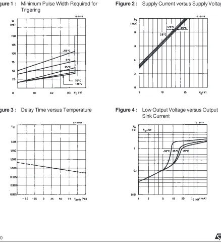
Figure 1 : Minimum Pulse Width Required for Trigering
Figure 2 : Supply Current versus Supply Voltage
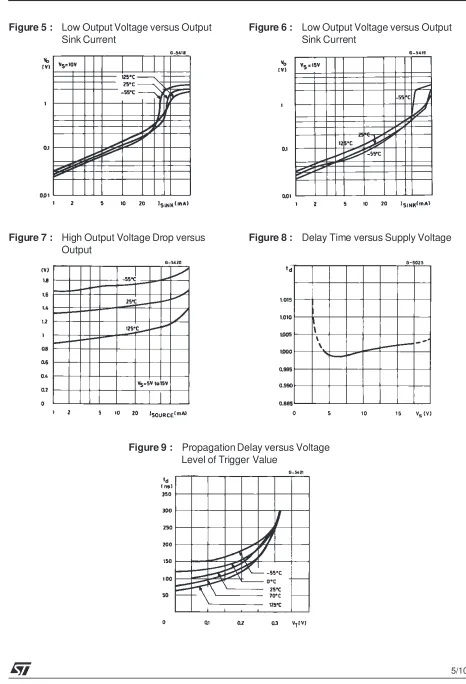
Figure 5 : Low Output Voltage versus Output Sink Current
Figure 6 : Low Output Voltage versus Output Sink Current
Figure 7 : High Output Voltage Drop versus Output
Figure 8 : Delay Time versus Supply Voltage
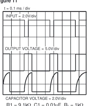
CAPACITOR VOLTAGE = 2.0V/div t = 0.1 ms / div
INPUT = 2.0V/div
OUTPUT VOLTAGE = 5.0V/div
R1 = 9.1kΩ, C1 = 0.01µF, R = 1kL Ω
Figure 11
Reset
Trigger
Output
R1
C1
Control Voltage
0.01µF
Figure 10
C
Figure 12 APPLICATION INFORMATION
MONOSTABLE OPERATION
In the monostable mode, the timer functions as a one-shot. Referring to figure 10 the external capaci-tor is initially held discharged by a transiscapaci-tor inside the timer.
The circuit triggers on a negative-going input signal when the level reaches 1/3 Vcc. Once triggered, the circuit remains in this state until the set time has elapsed, even if it is triggered again during this in-terval.The duration of the output HIGH stateis given by t = 1.1 R1C1and is easily determined by
figure 12.
Notice that since the charge rate and the threshold level of the comparator are both directly proportional to supply voltage, the timing interval is independent of supply. Applying a negativepulse simultaneously to the reset terminal (pin 4) and the trigger terminal (pin 2) during the timing cycle discharges the exter-nal capacitor and causes the cycle to start over. The timing cycle now starts on the positive edge of the reset pulse. During the time the reset pulse in ap-plied, the output is driven to its LOW state.
When a negativetrigger pulse is applied to pin 2, the flip-flop is set, releasing the short circuit across the external capacitor and driving the output HIGH. The voltage across the capacitor increases exponen-tially with the time constantτ= R1C1. When the
volt-age across the capacitor equals 2/3 Vcc, the
compa-ratorresets the flip-flop which then discharge the ca-pacitor rapidly and drivers the output to its LOW state.
Figure 11 shows the actual waveforms generatedin this mode of operation.
When Reset is not used, it should be tied high to avoid any possibly or false triggering.
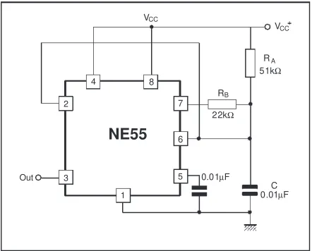
ASTABLE OPERATION
When the circuit is connected as shown in figure 13 (pin 2 and 6 connected)it triggers itself and free runs as a multivibrator. The external capacitor charges through R1and R2and discharges through R2only.
Thus the duty cycle may be precisely set by the ratio of these two resistors.
In the astable mode of operation, C1charges and
discharges between 1/3 Vccand 2/3 Vcc. As in the
t = 0.5 ms / div
OUTPUT VOLTAGE = 5.0V/div
CAPACITOR VOLTAGE = 1.0V/div
R1 = R2 = 4.8kΩ, C1= 0.1µF, R = 1kL Ω
Figure 14
C
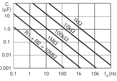
Figure 15 :Free Running Frequency versus R1,
R2and C1
Figure 14 shows actual waveforms generatedin this mode of operation.
The charge time (output HIGH) is given by : t1= 0.693 (R1+ R2) C1
and the discharge time (output LOW) by : t2= 0.693 (R2) C1
Thus the total period T is given by : T = t1+ t2= 0.693 (R1+ 2R2) C1
The frequency ofoscillation is them :
f=1 T=
1.44 (R1+2R2)C1
and may be easily found by figure 15. The duty cycle is given by :
D= R2
R1+2R2
Output 3
4 8
Figure 13
PULSE WIDTH MODULATOR
When the timer is connected in the monostable mode and triggered with a continuous pulse train, the output pulse width can be modulated by a signal applied to pin 5. Figure 16 shows the circuit.
Trigger
LINEAR RAMP
When the pullup resistor, RA, in the monostable
cir-cuit is replaced by a constant current source, a linear ramp is generated. Figure 17 shows a circuit con-figuration that will perform this function.
Trigger or equiv.
Figure 17.
Out
Figure 19 :50% Duty Cycle Oscillator.
Figure 18 shows waveforms generator by the linear ramp.
The time interval is given by :
T= (2/3 VCCRE(R1+R2)C
R1VCC−VBE(R1+R2) VBE=0.6V
Figure 18 :Linear Ramp.
VCC= 5V Top trace : input 3V/DIV Time = 20µs/DIV Middle trace : output 5V/DIV R1= 47kΩ Bottom trace : output 5V/DIV R2= 100kΩ Bottom trace : capacitor voltage RE= 2.7kΩ 1V/DIV
C = 0.01µF
50% DUTY CYCLE OSCILLATOR
For a 50% duty cycle the resistors RAand REmay
be connected as in figure19. The time preriod for the output high is the same as previous,
t1= 0.693 RAC. Thus the frequency of oscillation is f= 1
t1+ t2
Note that this circuit will not oscillate if RBis greater
than 1/2 RAbecause the junction of RAand RB
can-not bring pin 2 down to 1/3 VCCand trigger the lower
comparator.
ADDITIONAL INFORMATION
PM-DIP8.EPS
PACKAGE MECHANICAL DATA 8 PINS - PLASTIC DIP
Dimensions Millimeters Inches
Min. Typ. Max. Min. Typ. Max.
A 3.32 0.131
a1 0.51 0.020
B 1.15 1.65 0.045 0.065
b 0.356 0.55 0.014 0.022
b1 0.204 0.304 0.008 0.012
D 10.92 0.430
E 7.95 9.75 0.313 0.384
e 2.54 0.100
e3 7.62 0.300
e4 7.62 0.300
F 6.6 0260
i 5.08 0.200
L 3.18 3.81 0.125 0.150
Z 1.52 0.060
PM-SO8.EPS
PACKAGE MECHANICAL DATA
8 PINS - PLASTIC MICROPACKAGE (SO)
Dimensions Millimeters Inches
Min. Typ. Max. Min. Typ. Max.
A 1.75 0.069
a1 0.1 0.25 0.004 0.010
a2 1.65 0.065
a3 0.65 0.85 0.026 0.033
b 0.35 0.48 0.014 0.019
b1 0.19 0.25 0.007 0.010
C 0.25 0.5 0.010 0.020
c1 45o(typ.)
D 4.8 5.0 0.189 0.197
E 5.8 6.2 0.228 0.244
e 1.27 0.050
e3 3.81 0.150
F 3.8 4.0 0.150 0.157
L 0.4 1.27 0.016 0.050
M 0.6 0.024
S 8o(max.)
SO8.TBL
Information furnished is believed to be accurate and reliable. However, STMicroelectronics assumes no responsibility for the consequences of use of such information nor for any infringement of patents or other rights of third parties which may result from its use. No license is granted by implication or otherwise under any patent or patent rights of STMicroelectronics. Specifi-cations mentioned in this pub lication are subject to change without notice. This publication supersedes and replaces all infor-mation previously supplied. STMicroelectronics products are not authorized for use as critical components in life support devices or systems without express written approval of STMicroelectronics.
The ST log o is a trademark of STMicroelectronics
1998 STMicroelectronics – Printed in Italy – All Rights Reserved STMicroelectronics GROUP OF COMPANIES
Australia - Brazil - Canada - China - France - Germany - Italy - Japan - Korea - Malaysia - Malta - Mexico - Morocco
The Netherlands - Singapore - Spain - Sweden - Switzerland - Taiwan - Thailand - United Kingdo m - U.S.A. ORDER
CODE