TELKOMNIKA, Vol.10, No.3, September 2012, pp. 493~498 ISSN: 1693-6930
accredited by DGHE (DIKTI), Decree No: 51/Dikti/Kep/2010 493
Silicon Germanium Heterojunction Bipolar Transistor
for Digital Application
Engelin Shintadewi Julian
Department of Electrical Engineering, Trisakti University
Jl. Kiai Tapa No. 1 Jakarta Barat Indonesia 11410, Ph./Fax: +6221-5663232 ext 8433/ 5605841 e-mail: [email protected]
Abstrak
Kinerja transistor bipolar dinyatakan dengan figure of merit, antara lain: frekuensi cut-off, frekuensi osilasi maksimum dan emitter coupled logic gate delay. Pada makalah ini dibahas figure of merit yang tepat untuk aplikasi digital dan pengaruh penskalaan pada arah lateral serta vertikal terhadap figure of merit heterojunction bipolar transistor SiGe. Penskalaan pada arah lateral dilakukan dengan memperkecil lebar lengan emiter pada arah lateral dari 0,25 menjadi 0,12 µm sedangkan penskalaan pada
arah vertikal dititikberatkan pada penskalaan lebar basis. Juga dipelajari pengaruh bentuk profil Ge dan fraksi Ge pada basis. Penelitian dilakukan dengan perangkat lunak Bipole3 versi 5.3.1G. Simpulan penting yang dapat diambil antara lain: Heterojunction Bipolar Transsistor SiGe untuk aplikasi digital sebaiknya mempunyai frekuensi cutoff dan frekuensi osilasilasi maksimum yang tinggi serta emitter coupled logic gate delay yang rendah. Penskalaan pada arah lateral dapat meningkatkan frekuensi osilasi maksimum dan emitter coupled logic gate delay secara signifikan sedangkan penskalaan basis pada arah vertikal dapat meningkatkan frekuensi cutoff dan penguatan arus.
Kata kunci: HBT SiGe, basis SiGe, aplikasi digital
Abstract
Bipolar transistor performances can be characterized by figures of merit such as cut-off frequency, maximum frequency of oscillation and Emitter Coupled Logic gate delay. We studied the required figures of merit for digital application and the effects of lateral and vertical scaling to the figures of merit of SiGe Heterojunction Bipolar Transistor. With lateral scaling, the width of emitter finger is scaled down from 0.25 to 0.12 µm while with the vertical scaling, the base width is scaled down to reduce the
base delay. We also observed the effects of Ge profile and Ge fraction to the devices performances. Bipole3 5.3.1G is used to help us in the study. We found that high frequency cut-off and maximum frequency of oscillation as well as low Emitter Coupled Logic gate delay are all important for digital applications. Scaling down the emitter finger width enhanced the maximum frequency of oscillation and reduced Emitter Coupled Logic gate delay significantly while scaling down the base width increased the cutoff frequency and current gain.
Keywords: Silicon Germanium, SiGe, HBT, digital application
1. Introduction
The consumer demand for data from the internet, for digital audio and video is increasing rapidly [1]. According to Cisco Visual Networking Index (VNI) 2009 – 2014, the global internet traffic will increase more than fourfold to 767 exabytes or 767 million gigabytes or 2.1 million gigabytes daily by 2014. The traffic is dominated by video, exceeding 91% of global traffic as a result from improvements in network bandwidth capacity and internet speed along with the increasing popularity of High-Definition Television [2]. To support this growth of internet traffic, faster data transmission rate is needed.
needs of this new telecommu NF are the special concerns merit are more important in d SiGe HBT specific for digital a
2. Research Method We first study figures 12 – 18], and then determi applications design. Next, we SiGe HBT with emitter finger a
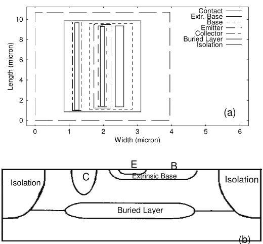
Figure 1. Schematic of (a)
BTs) could be used as medium and high power ap erformances can be characterized by figures of me c (ECL) gate delay. However, the relevance or
epends on the application [10]. In designing hig e of merit such as current gain β, early voltage VA
[11]. However, there are different opinions abou designing digital application. In this paper, we rep l application using Bipole3 device simulation softwa
s of merit of a bipolar transistor from published pap mines which particular figures of merit are imp
e define a reference device, which is basically a t r area AE 0.25x8 µm
2
as shown in Figure 1.
(a) lateral structure and (b) vertical cross section of devices
ertical doping and (b) Ge profile of the reference de
1 2 3 4 5 6 mportant for digital two base contacts
of the reference
TELKOMNIKA ISSN: 1693-6930 495
In the vertical direction, the reference device has 15 nm emitter widths with 1020 cm-3 peak doping concentration, 45 nm base width with 1.7x1019 cm-3 peak doping concentration and about 440 nm collector width with selected implanted collector (SIC) profile. The Ge profile in the base has trapezoid shape with 0.077 Ge fractions as shown in Figure 2. The reference device has 67 GHz peak fT, 65 GHz peak fMAX, 15 ps ECL gate delay, 3.6 Volt collector-emitter
breakdown voltages (BVCEO) and about 120 peak dc current gain (βDC). The reference device is
then scaled down laterally and vertically, and the scaling effects to the certain figures of merit are observed.
3. Results and Discussions 3.1. Figures of Merit
Researchers have different opinions in what particular figures of merit are required for digital application as shown below. According to Cressler, the fT and fmax cannot directly predict the performance of large-signal circuits, such as digital circuits, ECL ring oscillator speed or frequency divider data are more direct and accurate measure of digital switching speed [10]. For digital applications, a transistor is designed to function as a switch. One of the most important parameters for switching transistors is the minority carrier life time [12]. To increase the switching speed, one must increase the cutoff frequency [13, 14].
As SiGe HBTs are typically structured as a vertical device, their speed performance is mostly determined by the vertical transport of the carriers [15]. The common trend in HBT technology development is to achieve a device with balance fT and fmax. However, improvement in fT trades off and limits fmax of device [16]. Heterojunction bipolar transistor’s higher intrinsic fmax value, lower base resistance and lower substrate capacitance will permit higher speed for digital applications [17]. To achieve high switching speeds, it is not sufficient to just reduce the HBT’s dimensions, but the transistors parasitics like the base resistance or the collector-base capacitance must also be minimized [18]. For a digital circuit, the gate delay itself is often used as a figure of merit for the transistors in the circuit [10].
Based on the opinions stated above, we separate the parameters into input parameters and output parameters of the SiGe HBT design. The input parameters such as minority carrier life time, base resistance, substrate capacitance, device dimensions, collector-base capacitance can be controlled by adjusting the doping profiles and densities as well as device dimension in the vertical and lateral dimension. The output parameters such as the fT, fmax and ECL gate delay are the figures of merit that we need to observed and optimized.
3.2. Lateral Scaling
The emitter finger width (in the lateral direction) of the reference device is scaled down from 0.25 µm to 0.18 µm and 0.12 µm, while maintaining the emitter area at 2µm2,other lateral and vertical dimensions are preserved. We used Bipole3 automated mask option which only need the definition of emitter finger area as an input parameter. The other lateral dimensions are calculated automatically by Bipole3 and the detail of the device dimension can be observed at the output file.
The simulation results show that all SiGe HBTs have 3.6 Volt emitter-collector breakdown voltages BVCEO. The effects of lateral scaling to the SiGe HBTs fT and fmax at collector-base voltage VCB 1V are shown in Figure 3, for the ECL gate delay are shown in Figure 4, and the value of peak fT, fmax and βdc and the minimum ECL gate delays are presented in Table 1.
From Figure 3, Figure 4 and Table 1, we know that scaling down the emitter finger width enhance the maximum oscillation frequencies, lower the current gains and ECL gate delay, while the cut-off frequencies are stable at around 68 GHz. Scaling down the emitter finger width from 0.25 µm to 0.18 µm yields 24 GHz higher fmax and from 0.18 µm to 0.12 µm gives us another 37 GHz enhancement. Further observation shows that SiGe HBT with narrower emitter finger has smaller base resistance and according to Eq. (1), smaller base resistance yields higher fmax. Our results are consistent with previous research by Zhang et.al. [19].
2 / 1
max
8
=
bc b
t
C
R
f
f
Figure 3. The ft and fmax curve of SiGe HBTs with emitter area AE 0.25x8, 0.18x11 and
0.12x17µm2 at VCB=1V
TELKOMNIKA ISSN: 1693-6930 497
other delays at high current. The base width is scaled down from 45 nm to 36 nm and then to 30 nm. The effects of base width to the SiGe HBT figures of merit are shown in Table 2. Scaling down the base width from 45 to 30 nm enhances the peak fT of SiGe HBT around 15% from 67 to 77 GHz. Reduction in vertical delay is the main contributor to enhance the fT of SiGe HBTs with narrower base width. Base width scaling also has the same effects to the βdc with enhancement in current gain about 45%. Table 2 also shows that scaling down the base width has stronger effects to the fT and βdc but weaker to the fmax and ECL gate delay.
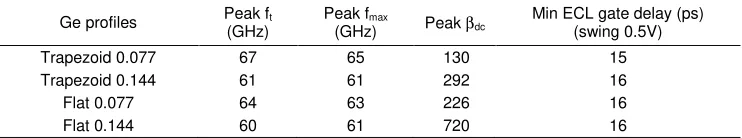
Besides the flat shape Ge profile with 0.077 and 0.144 Ge mole fraction, the trapezoid shape Ge with 0.077 and 0.144 peak Ge mole fraction in the base are also observed. The Ge profiles in the base are shown in Figure 5. The effects of Ge profile in the base of SiGe HBT to the device performances are summarized in Table 3.
For both Ge profiles, higher Ge mole fraction yields lower peak fT and fmax. Our results show that SiGe HBTs with trapezoid Ge profiles have higher cutoff frequencies and higher maximum frequencies of oscillation, but lower current gain compared to SiGe HBT with flat Ge profiles ,which is consistent with previous research [20, 21], which used trapezoid Ge profil for optimum SiGe HBT performance. The simulation results show that base width scaling, Ge profiles and Ge mole fraction have no significant effect to the ECL gate delay.
Figure 5. Ge profiles in the base of SiGe HBTs (base width 45nm and AE=0.25x8µm
2 )
Table 3 The effects of Ge profiles and mole fraction to the SiGe HBT performance
Ge profiles Peak ft (GHz)
Peak fmax
(GHz) Peak βdc
Min ECL gate delay (ps) (swing 0.5V) Trapezoid 0.077 67 65 130 15 Trapezoid 0.144 61 61 292 16
Flat 0.077 64 63 226 16
Flat 0.144 60 61 720 16
4. Conclusion
Scaling down the emitter finger width in the lateral direction enhance the maximum frequency of oscillation due to smaller base resistance and reduce the ECL gate delay. However, it also decreases the current gain while the cut-off frequencies are steady. Scaling down the base width enhance the cutoff frequency of SiGe HBT due to reduction in vertical delay. Base width scaling also enhances the current gain. Base width scaling has stronger effects to the fT and βdc but weaker to the fmax and ECL gate delay. SiGe HBTs with trapezoid
Ge profiles have higher cutoff frequencies and higher maximum frequencies of oscillation but lower current gain compared to SiGe HBT with flat Ge profiles. Base width scaling, Ge profiles and Ge fraction have no significant effect to the ECL gate delay.
0 0.02 0.04 0.06 0.08 0.1 0.12 0.14 0.16
0 0.1 0.2 0.3 0.4 0.5 0.6
G
e
f
ra
c
ti
o
n
Depth (microns)
References
[1] Wolf S. Silicon Processing for the VLSI Era: Vol. 4 - Deep Submicron Technology. California: Lattice Press. 2002.
[2] Noname. Annual Cisco Visual Networking Index Forecast Projects Global IP Traffic to Increase More Than Fourfold by 2014. Cisco Press Release. June 2010.
[3] Noname. Path to 100G, Fujitsu Network Communications, Inc Whitepaper. 2011.
[4] IEEE Standards Committee. 802.3ba-2010. IEEE Standard for Information technology -
Telecommunications and information exchange between systems - Local and metropolitan area networks - Specific requirements Part 3: Carrier Sense Multiple Access with Collision Detection (CSMA/CD) Access Method and Physical Layer Specifications. New York: IEEE Press; 2010.
[5] Griffith Z, Dahlström M, Rodwell MJW, Fang X-M, Lubyshev D, Wu Y. Fastenau JM, and Liu WK. InGaAs–InP DHBTs for Increased Digital IC Bandwidth Having a 391-GHz ft and 505-GHz fmax. IEEE Electron Devices Letter. 2005; 26(1): 11-13.
[6] Rieh J-S, Jagannathan B, Chen H, Schonenberg K, Jeng S-J, Khater M, Ahlgren D, Freeman G, and Subbana S. Performance and design considerations for high speed SiGe HBTs of fT/fMAX = 375 GHz/210 GHz. Proceedings of the IEEE International Conference On Indium Phosphide and Related Materials. Santa Barbara. 2003; 374-377.
[7] Rieh J-S, Jagannathan B, Chen H, Schonenberg K, Angell D, Chinthakindi A, Florkey J, Golan F, Greenberg D, Jeng S-J, Khater M, Pagette F, Schnabel C, Smith P, Stricker A, Vaed K, Volant R, Ahlgren D, Freeman G, Stein K, and Subbana S, SiGe HBTs with cut-off frequency of 350GHz. International Electron Devices Meeting Technical Digest. San Fransisco. 2002; 771-774.
[8] Nahri DG, Arabshahi H. Static Characterization of InAs/AlGaAs Broadband Self- Assembled Quantum Dot Lasers. TELKOMNIKA. 2012; 10(1), 55-60.
[9] Suroso, Noguchi T. Five-Level Common-Emitter Inverter Using Reverse-Blocking IGBTs. TELKOMNIKA. 2012; 10(1), 25-32.
[10] Taur Y and Ning TH. Fundamental of Modern VLSI Devices. Second Editions. Cambridge: Cambridge University Press. 2009.
[11] Harame DL, Comfort JH, Cressler JD, Crabbe EF, Sun JY-C, Meyerson BS, Tice T. Si/SiGe Epitaxial Base Transistors – Part II : Process Integration and Analog Applications, IEEE Trans. on Electron Dev. 1995; 42(3): 469-482.
[12] Cressler JD and Niu G. Silicon Germanium Heterojunction Bipolar Transistor. Massachusette: Artech House. 2003.
[13] Sze SM. Semiconductor Devices Physics and Technologies. Singapore: John Wiley & Sons. 1985. [14] Sze SM. Physics Semiconductor Devices. 2nd Edition. New York: John Wiley & Sons. 1982.
[15] Rieh J-S, Khater M, Jeseph A, Freeman G and Ahlgren D. Effect of Collector Lateral Scaling on Performance of High-speed SiGe HBTs with ft > 300GHz. Electronics Letters. 2006: 42(20).
[16] Khater MH, Adam TN, Khrisnasamy R, Dahlstrom ME, Rieh J-S, Schonenberg KT, Orner BA, Pagette F, Stein K, Ahlgren DC. Present Status and Future Directions of SiGe HBT Technology. International Journal of High Speed Electronics and System. 2007; 17(1): 61-80.
[17] Yuan JS. SiGe, GaAs, and InP Heterojunction Bipolar Transistors. New York: John Wiley and Sons. 1999.
[18] Stricker AD, Freeman G, Khater M, Rieh J-S. Evaluating and designing the optimal 2D collector profile for a 300GHz SiGe HBT. Materials Science in Semiconductor Processing. 2005; 8: 295–299.
[19] Zhang S, Niu G, Cressler JD, Joseph AJ, Freeman G, and Harame DL. The Effects of Geometrical Scaling on the Frequency Response and Noise Performance of SiGe HBTs. IEEE Trans on Elect. Dev. 2002; 48(3): 429-435.
[20] Richey DM, Cressler JD, and Joseph AJ. Scaling Issues and Ge Profile Optimization in Advanced UHV/CVD SiGe HBT’s. IEEE Trans on Electron Dev. 1997; 44(3): 431 – 439.