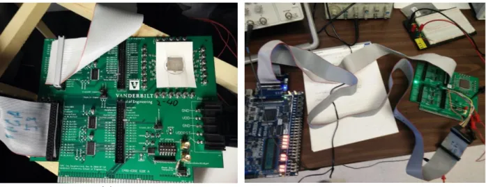
I would also like to thank the co-authors of the article [1] on which much of this work is based, especially Dr. If an incorrect voltage at the input of one of the inverters in this loop persists long enough, it can lead to an incorrect output propagating to and through the second inverter, maintaining the initial incorrect voltage. 8 3.1: Images of (a) a close-up of the test board and (b) the test board connected to an FPGA for alpha particle testing.
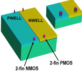
The impact site for all simulations was the center of one of the NMOS fins. The rapid growth of the private aerospace industry has fueled the demand for faster and cheaper spacecraft development, which in turn has led to increasing interest in the use of commercial off-the-shelf (COTS) parts due to their superior performance and lower cost. compared to parts of space equipment. The threshold energy required to generate an EHP depends on the gap energy of the irradiated material.
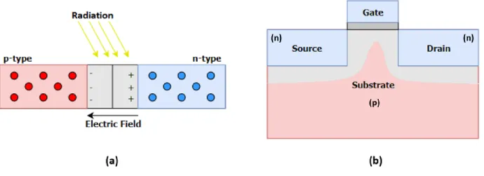
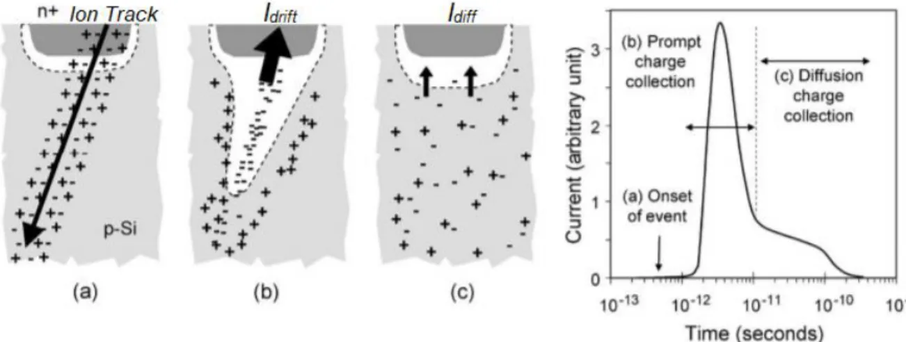
The band gap of silicon is approximately 1.1 eV, but some of the energy from the incident particles is absorbed as heat, so the threshold energy to create an electron-hole pair in silicon is approximately 3.6 eV [19]. Drift refers to the movement of charge carriers due to an electric field, and diffusion refers to the movement of charge carriers due to the counter gradient of the carrier concentration. Transient voltages are not faults per se, but they may cause faults if they change the state of the circuit in some way.
If the voltage pulse is not masked by one of the above methods, it may be stored in the latch as false data.
FinFET Structure
In a bulk FinFET, the only path to the substrate is through a narrow neck region, making charge collection much less efficient than in planar MOSFETs, where the source and drain are completely contained within the substrate/well [17]. This is illustrated in Figure 2.4, which shows how charge deposited in the substrate can diffuse freely to the drain in the planar structure, but charge must diffuse through the neck region in the FinFET structure because all other paths are blocked by the shallow trench insulation. (STD).
Designing for Low-Power
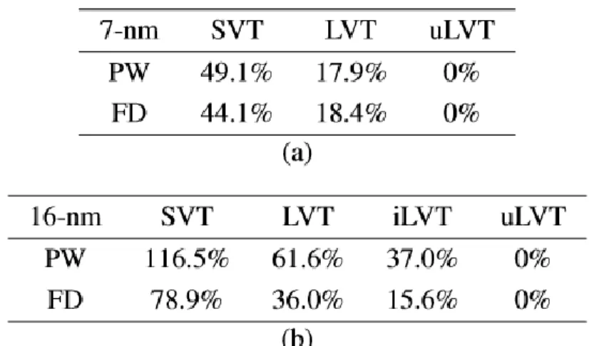
Often this trade-off can be solved locally and lower supply voltages and higher cut-off voltages can be used in sub-circuits with relatively favorable timing requirements. In the case of FinFETs, this option is very attractive due to their excellent performance at low supply voltages, which in turn provides greater design flexibility. In addition to power consumption, SET PW and FF FD are also strongly related to the selected VT option for the logic gate.
How effectively the junction can be restored depends on how quickly this transistor can sweep away excess charge carriers, and the rate at which this happens is the transistor saturation current. This relates VT and SE cross sections because increasing VT reduces the drive/saturation current, as shown by the ID equation above, resulting in an increase in SET PW and a corresponding increase in SE cross section. Increasing VT also increases FF FD due to the increased gate delays, resulting in a decrease in SE cross section.
If mean PW increases faster than FD as VT increases, SEUs should become more likely because PW SET becomes more likely to be longer than FD; the opposite is true if the mean FD increases faster.
Test Circuit
The overall design for the test circuit applies the Circuit for Radiation Effects Self-test (CREST) architecture [32], as shown in Figure 3.2. Whenever a DFF in one of the shift registers breaks, the returned bit is propagated through the register and counted by the error counter when it does not match the expected output from the input data source. All circuitry that is not part of the shift registers uses triple modular redundancy (TMR) to protect against spurious error counts.
This approximation is reasonable because if the number of errors is greater than ten, the 1-σ Gaussian statistical limit approaches both the upper and lower Poisson statistical limits with at least one digit accuracy [34]. All heavy ion tests were performed at Lawrence Berkeley National Laboratory (LBNL) with a 16 MeV/nucleon cocktail, the components of which are shown in Table 3.1, with values calculated using SRIM. During the tests, the shift registers were given the input “0” and clocked at a frequency of 2.5 MHz.
Keeping the input voltage to the shift registers at 0 V during testing prevents ion spikes within the clock tree from resulting in disturbances because a high value cannot be written to a flip-flop due to a false positive signal. high hour, ensuring that all concerns are observed. are due to ion collisions within a latch cell. Alpha particle tests were performed at Vanderbilt University using a 1 cm × 1 cm 241Am sheet source positioned less than 1 mm away from the head, in accordance with the JESD89 standard [37]. The results in this paper come from tests performed at room temperature with a particle flux of 1000 alpha/mm2/s.
![Figure 3.2: Block diagram of CREST configuration used in SEU test circuit. After [35]](https://thumb-ap.123doks.com/thumbv2/123dok/10740469.0/18.918.108.809.615.916/figure-block-diagram-crest-configuration-used-seu-circuit.webp)
Schematic Simulations
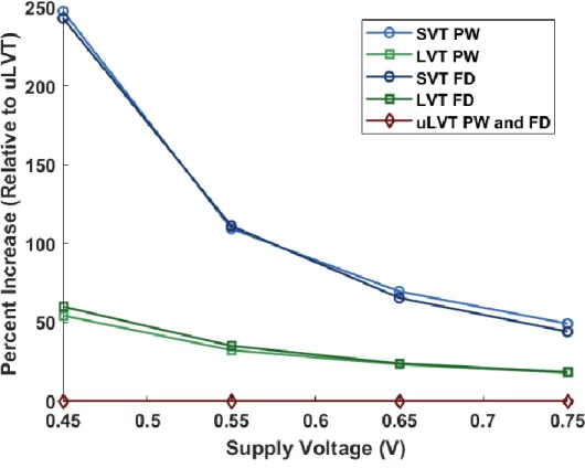
Therefore, for particles with high LET values, reducing the drive current by reducing the supply voltage and increasing the threshold voltage can greatly affect the SEU cross section. At a supply voltage of 0.75 V (nominal), all designs show a very similar SE cross section for alpha particles (Figure 5.1(a)). In these results, the much stronger dependence on supply voltage, shown by the nearly 25-fold increase in the cross-section for SVT as the supply voltage drops from nominal to 0.45 V, completely overshadows any dependence of the SEU cross-section on the choice of VT.
At a supply voltage of 0.45 V, the point of greatest difference between the SVT and uLVT cross-sections, the SVT cross-section is only approx. 2× larger than the uLVT cross-section. For high-LET particles, SE cross-sections are subject to the transistor drive current trend—increasing drive current leads to decreasing SE cross-sections. At a LET value of 24.98 MeV-cm2/mg, the average SVT cross section at a supply voltage of 0.45 V is more than 5× larger than the average SVT cross section at nominal supply.
For particles with low LET values, this dependence is even stronger, with the uLVT cross section increasing by about 25× as the supply voltage decreases from 0.75 V to 0.45 V. These three distinct behaviors clearly illustrate the point that the effects of VT options on the cross-sectional SEU must be evaluated for each new technology node. However, it is worth noting that for higher LET values and lower than nominal biases, the 7 nm heavy ion results follow the same trend as the 16 nm alpha results, which is that the SEU cross section increases with threshold voltage.
SE cross section as a function of particle LET may be related to mechanistic differences in how particle strikes cause disruptions at different LET values. In the 20-nm technology, SEU cross-section decreases as VT increases, while in the 16-nm technology, SEU cross-section increases with VT. Consequently, small differences in critical load for different VT options become significant in determining SE cross-section.
Since the critical load is inversely proportional to VT values, the uLVT design shows the lowest SE cross section and the SVT design shows the highest SE cross section. This dependence is quantified for all VT options and both low-LET (alpha-particle) and high-LET (Krypton) particles in Table 6.1, which shows the ratio of the SEU cross-section at given supply voltages to the corresponding SEU cross-section at nominal supply . As for high-LET particles, the presence of the VT tendency is conditional on the supply voltage being lowered, although the dependence of the SEU cross-section on supply voltage is weaker than it is for low-LET particles.
Since the drive current is roughly quadratically dependent on the difference between the supply voltage and VT (from the saturation current equations), the percentage difference between the drive currents of different VT options will also be greater when the supply voltage is lower, which in turn leads to larger differences in the SEU cross-section. In general, the trade-off between SEU cross-section and VT must be taken into account for designs that must withstand high-LET particle attacks at supply voltages below the rated voltage. For the 7-nm technology used in this paper, the SEU cross-section is largely independent of the threshold voltage.
Only when the supply voltage is low and the particle LET is high does a trend appear that the SEU cross-section is directly related to threshold voltage.
![Figure 2.4: Comparison of (a) FinFET and (b) planar structures. From [29].](https://thumb-ap.123doks.com/thumbv2/123dok/10740469.0/14.918.108.803.414.800/figure-2-4-comparison-finfet-planar-structures-29.webp)
![Table 3.1: 16 MeV/Nucleon Cocktail Components [36]](https://thumb-ap.123doks.com/thumbv2/123dok/10740469.0/19.918.98.814.757.972/table-3-16-mev-nucleon-cocktail-components-36.webp)