3.3(b) and (b) Vth shift as a function of dose and annealing at room temperature for transistors from the same wafer ..29 3.5. Radiation-induced charge density as a function of dose and annealing at room temperature in the flat band for the devices of Fig.
![Fig. 1.1. Schematic diagram illustrating physical processes for radiation-induced charge generation in MOS capacitor [3]](https://thumb-ap.123doks.com/thumbv2/123dok/10733416.0/10.918.204.719.212.536/schematic-diagram-illustrating-physical-processes-radiation-generation-capacitor.webp)
Device Characteristics
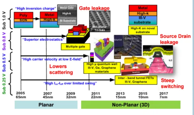
High-K Dielectrics
Since capacitance is inversely proportional to thickness, to increase gate capacitance and improve device performance, SiO2 thickness must be reduced. In most cases, the thickness of high-k dielectrics is greater than that of SiO2, which reduces the leakage current and improves the dielectric reliability of the gate [31], [32].
Ge and III-V Channel
However, when the thickness of SiO2 goes below 1.4 nm, the electron tunneling effects and high leakage current will cause a decrease in device reliability [30]. In this circumstance, high-k dielectrics become a potential substitute due to its higher dielectric constant at an acceptable thickness.
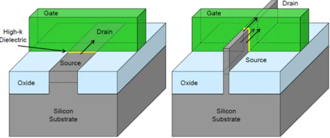
FinFET Structure
Overview of Thesis
For this InGaAs technology, lower radiation-induced defect densities are estimated for capacitors than for transistors, indicating that transistor response is likely to be improved with future optimization of the technology. In this chapter, we describe the capacitance-voltage (C-V) and capacitance-frequency (C-f) techniques and illustrate the method for MOS capacitors with relatively thick SiO2 gate dielectrics.
Mechanism of C-V Measurement
When a voltage is applied to the gate, the voltage is dropped partly across the oxide and partly across the semiconductor. Therefore, the capacitance of the MOS device is the oxide capacitance Cox in series with the semiconductor capacitance Cs. As the gate voltage changes, the variation of the semiconductor surface potential and space charge area distribution results in three different situations: accumulation, depletion, and inversion.
Because the oxide thickness and dielectric constant of the oxide remain unchanged, the capacitance in the accumulation region remains the same (see accumulation region in Figure 2.1). Since the total capacitance is the oxide capacitance in series with the capacitance in the depletion region in Eq. 2), the total capacitance value is reduced. Since the semiconductor capacitance is inversely proportional to the depletion width in Eq. 3), the total capacity decreases as the depletion layer increases (see the depletion region in Figure 2.1).
Therefore, the total capacitance for high frequency Cox in series with Cs in Eq. No matter how the gate voltage changes, the C-V curves in this case remain minimal (see the high-frequency curve in Figure 2.1).
![Fig. 2.1. C-V curves in low- and high-frequency of a MOS capacitor on a n-type substrate [43].](https://thumb-ap.123doks.com/thumbv2/123dok/10733416.0/19.918.188.710.321.578/fig-curves-high-frequency-mos-capacitor-type-substrate.webp)
Experiment Setup
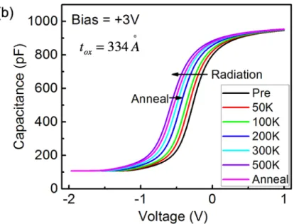
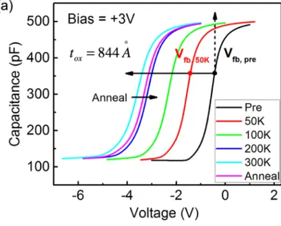
Arrows at flatband in (a) show schematically that net hole trapping causes the capacitance at flatband to increase with dose at constant voltage and shift the C-V curve to the left at constant capacitance. Using the midgap technique of Winokur et al. 1], the net radiation-induced oxide precipitation charge density, projected to the Si/SiO2 interface, can be estimated from high-frequency C-V curves via [1]:. In the limit of small variations around Vfb, additional hole trapping causes the capacitance to increase when the voltage is kept constant in the same way that it causes curves to shift to the left when capacitance is kept constant (Fig. 2.4 a).
In contrast, an increase in negative charge will cause the capacitance at fixed voltage to decrease in the same way that it shifts the curve to the right at fixed capacitance, as confirmed below. This increase in capacitance with decreasing frequency occurs due to (1) an increase in boundary-trap density with increasing dose, and (2) the increasing sensitivity of The increase in boundary trap charge density with decreasing frequency has been exploited in previous combinations of I-V, charge pumping, and low-frequency noise measurements to provide quantitative estimates of effective boundary trap charge densities.
But so far this simple technique has not been adapted to estimate the limiting trap densities in irradiated MOS capacitors via C(f) measurements. When there is a measurable difference between values of C(f) at high and low frequencies, an estimate of the effective limiting density Nbt,C-f before and after irradiation before irradiation and at each dose level can be obtained from a simple expression: is analogous to Eq . 4), but adapted for use with a fixed voltage and varying capacity:
Correction Factor
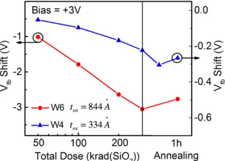
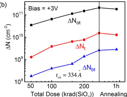
Prior to irradiation, the threshold trap densities below the detection threshold cm-2 for these devices and measurement conditions are estimated. These are lower estimates of the density of fast boundary traps [19], since the C-f measurements cover only about 3 decades of the response. Irradiation-induced charge densities as a function of dose and annealing at room temperature at flat band for (a) W6 and (b) W4 irradiated and annealed at room temperature with VG = +3 V.
The effective pre-radiation boundary trap density is less than 2-3×108 cm-2 in each device, which is approximately our threshold for detectability via C-f measurements. Inferred density of boundary traps and ratios to interface charge density in Figs. 2.7 are comparable to previous work on Si MOS transistors with similar oxides using I-V, charge pumping, and/or 1/f noise measurements reinforcing the utility of this approach. We therefore restrict the use of Eqs. 7) and (8) for boundary trap density estimates in relatively thick SiO2 oxides (Figures are applied to the remainder of the tested devices, with no attempt at adjustment.
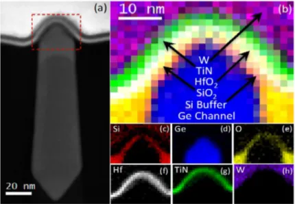
This chapter presents a method applied to multi-fin capacitors built in state-of-the-art strained Ge pMOS FinFET technology with a Si overlayer and SiO2/HfO2 gate dielectric. The device information is shown first, and the C-V and C-f results for those devices are shown later.
Device Information
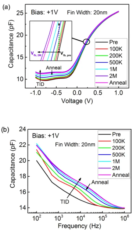
The fin width for the first and third rows increases from the first element to the tenth, and decreases. 3.3 (a) shows schematically that net negative charge capture causes the flatband capacitance to decrease with dose at constant voltage and the C-V curve to shift to the right at constant capacitance. At +1 V irradiation, larger shifts are found than at 0 V bias, without significant effects on the fin width (μm). of the observed geometry, consistent with trends for FinFETs in [14]. a) High-frequency CV curves as functions of dose and glow at room temperature for a two-fin capacitor with a lamella length of 12.5 µm and a lamella width of 75 nm at gate bias VG = +1V, and (b).
Vfb shifts as a function of dose for gate biases VG = 0 V and +1 V, and room temperature annealing up to 12 h for. 3.4(a) shows the flatband, midband, and reverse voltage shifts for a 50 nm fin-width device irradiated at +1 V. The similarity of the midgap and flatband shifts suggests that the trap charge oxide is more important than the interface trap charge in these devices. The results for pMOS transistors built in the same FinFET technology are shown for comparison in Fig.
Therefore, capacitors and transistors for these Ge pMOS devices show similar radiation responses. a) Vth, Vfb and Vmg shifts as functions of dose and room temperature annealing for the device showing the worst shifts in Fig. These devices show net negative charge trapping under irradiation; consequently, the flatband capacitance decreases with dose in Fig.
Estimating Trapped Charge Densities
This chapter introduces the method applied to capacitors and transistors built in an early stage of development InGaAs FinFET technology with Al2O3/HfO2 dielectric layers. The device information is illustrated first, and C-f results and radiation-induced trap charge estimates for these devices are shown later. The capacitors range in InGaAs fin width from 20 nm to 26 nm and have a fin length of 5 µm.
The transistors presented in this work have a fin width of 26 nm and a fin length of 5 µm. The bottom contact connects the channel (body) through the substrate for Ge MOS capacitors, and to the channel (body) directly from a top contact for InGaAs MOS capacitors. The network representation of the test structure of multi-threaded capacitors is the same as Fig.
The fin width for the first and third rows increases from the first to the tenth element, and decreases for the second and fourth.
Buffer
Total Ionizing Dose Effects on InGaAs Capacitors
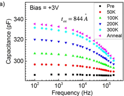
The capacitance increases with decreasing frequency even before the devices are irradiated, consistent with a significant boundary drop density cm2) in these devices before irradiation. There is a large shift due to radiation-induced oxide precipitation, consistent with significant hole trapping in these Al2O3/HfO2 hexastacks [57]. The increase in boundary trap density in these devices at 2 Mrad(SiO2) is similar to the as-processed density of boundary traps.
Radiation-induced charge density as a function of dose for the devices and irradiation conditions of Fig. Again, a large initial boundary trap density and significant radiation-induced shifts are observed, with hole trapping dominating the radiation-induced shifts and boundary traps comprising a fraction of the stretch in C-V measurements. Of the C-V curves, hole trapping dominates radiation-induced shifts and boundary traps account for a significant portion of the stretch in C-V measurements. a) High frequency (1 MHz) C-V curves and (b) C-f curves as functions of dose and chamber.
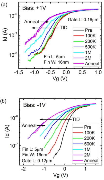
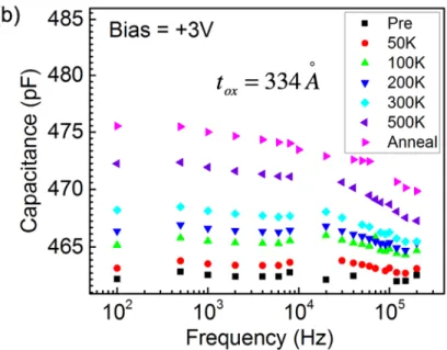
4.11(a) shows flatband, midgap, and inversion voltage shifts for a 16-nm fin width device irradiated at 0 V. The capacitance increases with decreasing frequency even before the devices are irradiated, consistent with a significant boundary drop density cm- 2) in these devices before irradiation.
Total Ionizing Dose Effects on InGaAs Transistors
Schrimpf, et al., “Fin Width Dependence of Ionizing Radiation-Induced Subthreshold Oscillation Degradation in 100-nm Gate-Length FinFETs,” IEEE Trans. Paillet, et al., “Radiation Effects in Advanced Silicon Insulator Multigate Transistors,” IEEE Trans. Zhang, et al., “Bias Dependence of Total Ionizing Dose Effects in SiGe-SiO2/HfO2 pMOS FinFETs,” IEEE Trans.
Hachtel, et al., “Effects of total ionizing dose on biased Ge pMOS FinFETs on bulk Si,” IEEE Trans. Zhao et al., “Hysteresis in Lanthanide Aluminum Oxides Observed by Fast Pulse CV Measurement,” Mater., vol. Xu et al., “Polarity effect on temperature dependence of leakage current through HfO2/SiO2.
Massengill et al., “Heavy ion-induced degradation in ultrathin gate oxides and high-k dielectrics,” IEEE Trans. Yu, et al., “A distributed model for boundary traps in Al2O3-InGaAs MOS devices,” IEEE Electron Device Lett., vol.