The spikes are the result of the 60-Hz lift and are ignored in the data fitting and analysis. Log-log plot of noise power spectral density versus Vds2/(Vgs-Vth)2 for the data. A significant fraction of the radiation-induced residual charge can be trapped in microstructural defects in the dielectric.
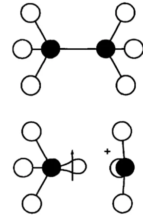
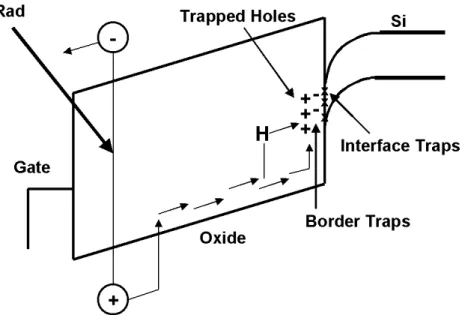
Some of the unrecombined holes will become trapped in the oxide, creating a positive oxide trapped charge density. 3 shows a diagram of the E0γ trapping center, where part (a) represents the oxide trap precursor (O3≡Si-Si≡O3) and part (b) shows a hole trapped by the precursor site (O3≡Si↑+ Si ≡O3). This probably occurs because hydrogen released in the bulk of the dielectric or near the interface (which is responsible for the build-up of interfacial traps in thermal oxides) cannot penetrate into the nitrogen-rich oxynitride layer near the interface and can create interfacial traps [104].
The bias dependence of the hysteresis suggests that it is related to electron movements into and out of boundary traps in the near interfacial region of the oxide [106]. However, my results showed that the interfacial oxynitride plays an important role in the breakdown of the dielectric stacks for these devices. As discussed in detail below, similar processing effects are also observed for the radiative response of the nMOSFETs versus the capacitors.
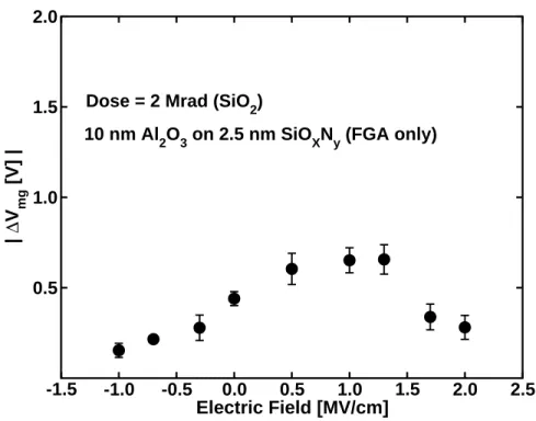
7 is a plot of the absolute value of ∆Vmg after a total dose of 2.0 Mrad(SiO2) as a function of the electric field of the oxide during irradiation.
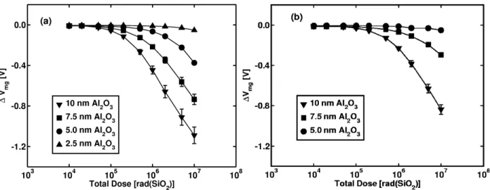
Therefore, most of the measurable trapping in these devices occurs in the Al2O3 as the charge trapped in the oxynitride is removed due to tunneling. As shown in Fig. 12, for negative bias exposures there is almost the same radiation response for devices with the same Al2O3 thickness, independent of the boundary oxynitride. Shallow trapped electrons can easily move in and out of the gate dielectric, causing effects such as CV hysteresis [120].
The 1/f noise of the packaged devices was measured as a function of both drain voltage (Vds) and gate voltage (Vgs). 14 is a plot of the surge noise power spectral density SV as a function of frequency for (a) several drain voltages at a constant Vgs of 5 V and for (b) varying Vgs with a constant Vds. As a guide to the eye, a set of parallel lines has been added to the pre-irradiation and 1 Mrad(SiO2) curves to show that, as with the CV curves of the capacitors, there is no measurable stretching due to interface traps in these devices.
Therefore, these results differ significantly from previous experiences on the radiative response of the Si/thermal SiO2 system. 17 and 19, it can be hypothesized that the surprising results of Figure 19 are related to hydrogen passivation of some of the boundary traps and/or interfacial defects in these devices. Thus, it is possible that some of the hydrogen in these films is released during irradiation and passiveizes defects at or near the interface.
Therefore, instead of the reaction shown in equation 4, it is possible that the mechanism for interface passivation in these devices could be something like this. The hafnium silicate gate dielectric was deposited using CVD after a wet etching of the field insulating oxide. The backside of the wafer was then sputtered with aluminum to allow electrical contact with the substrate.
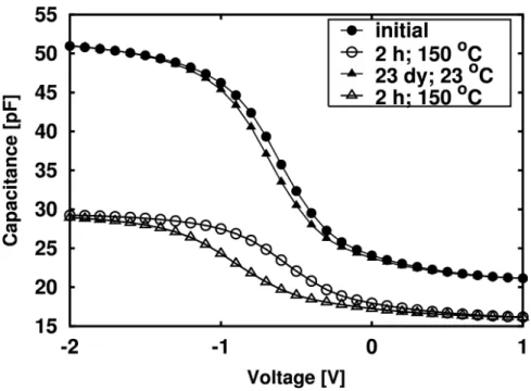
Vf b there is no measurable interfacial trap build-up with ionizing radiation for these devices within the accuracy of the measurement. The effect of these charges can be seen from the relatively large extent of the pre-irradiation curve in Fig. The data in these figures represent the average of the results from ~5 capacitors for each bias condition.
24, the amount of CV hysteresis was inversely proportional to the magnitude of the radiation voltage shift. This processing dependence certainly warrants further study and may crucially depend on the relative amounts of holes and electron traps in the near interfacial region of the gate dielectrics.
This definition is consistent with the concept of EOT, which describes what the thickness of the dielectric would be if it were SiO2 instead of an alternative dielectric, based on the measured capacitance value. Disregarding possible dose-enhancing effects, the effective trapping efficiency can be estimated for an alternative dielectric film using Some of the quantities in Equation 6, such as κgandfy, are not known for many alternative dielectrics.
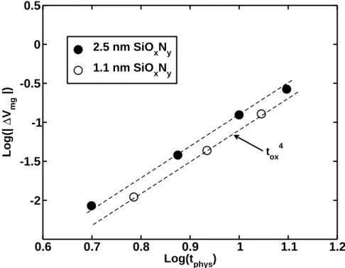
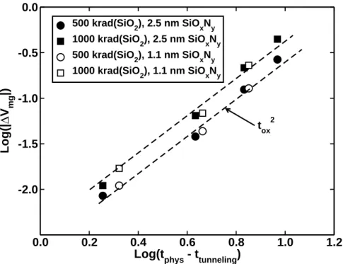
However, the idea of Equation 6 is to leverage the extensive knowledge about SiO2 to get a reasonable estimate of the effective capture efficiency for these new materials [42]. In Equation 6, the physical term takes into account the generation of charge throughout the entire volume of the oxide. As mentioned in Chapter III, charge in the near interfacial region of the dielectric can be removed via tunneling, effectively diluting the gate dielectric with the tunneling distance into the gate dielectric.
The term Theteq takes into account the moment arm effect resulting from the projection of the spatial distribution of charges in the oxide onto the interface [113]. To understand this, it is important to know that one charge at the interface has the same effect (electrically) as two charges in the middle of the dielectric. Therefore, if the location of the center of charge were known, it would be appropriate to add a scale factor to the numerator of equation 6 (ie 2 if the center is in the middle of the dielectric).
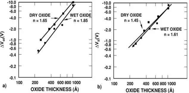
In some cases this is by design (e.g. the devices of Chapter III) to improve the quality of the interface, but there is also the possibility of inadvertent surface oxidation of the Si substrate during processing. This creates a "parasitic" layer of SiO2 at the interface, resulting in an overall reduction. The location of the center of charge of the trapped oxide after exposure to ionizing radiation depends on the irradiation bias conditions [146, 147].
For low electric field and zero volt biased exposures, the charge centroid will tend to be towards the center of the dielectric. Fleetwood [147] developed a method to calculate the location of the charge centroid using TSC and CV analysis. To calculate the true trapping efficiency of a high-k material, it is necessary to carry out more rigorous studies to determine factors such as κg and fy, and it is also important to account for effects such as the location of the charge centroid and dielectric stack structures.

Similar changes in the CV curves of hafnium silicate were commonly observed in the tested devices. One possible reason for this effect is that the reduction and subsequent recovery of capacitance in these devices may be due to water vapor being baked and reabsorbed by these films [151]. Indeed, a chemical change appears to occur in these devices in the absence of water vapor; however, a more detailed baking study is still needed to fully determine the cause of the baking effect observed in Figure 2.
Charge injection and blocking can also cause a misinterpretation of the radiation response of an alternating gate dielectric. The characteristic time t = α is often called "T63". The experimental lifetime of oxides subjected to constant electric fields large enough to cause oxide breakdown on laboratory time scales is usually determined by making Weibull probability plots of the data, i.e., plots of Wf(t) = ln(- ln(1-F( t)) vs. ln(t) The functional form of the dependence of T63 on electric field and temperature has been controversial, especially with respect to the shape of the electric field acceleration parameter.
The field and temperature dependence of the time to degradation has been modeled by McPherson [152, 153]. Examples of dielectric breakdown in two modes (intrinsic and extrinsic) where the extrinsic part of the distribution is visible are shown in the 4.0 MV/cm and 4.5 MV/cm data in Figure. It is not clear whether the early disturbances in the large electric field data are the result of this.
29, it is possible to see that the outer error population constitutes almost 30% of the total sample set for the two lowest electric fields. The manual fit was performed by forcing the intrinsic part of the distribution to have the same slope (0.9) as the single-mode error data, while varying the other Weibull parameters until the fit appeared to match the data. Calculating effective capture efficiencies allows the capture properties of multiple materials to be compared without having to know all the material properties of each new material.
Increasing the trapping efficiency from 1% to 12% or 30% means that alternative gate dielectrics will trap about 11% to 29% more initial charge than thermal SiO2 of comparable electrical thickness. It has also been shown that radiation testing at large gate biases can lead to excessive bias induced charge trapping and possible overestimation of the radiation hardness of the alternative dielectric. Phenomenon of charge carrier transfer in amorphous SiO2; direct measurement of drift mobility and lifetime.
Effect of ion energy on dielectric breakdown of capacitor response in vertical power MOSFETs. Fundamental physics of the thermochemical modelE in the description of low-field time-dependent dielectric breakdown in SiO2 films.