Financial support for this work was provided by the Department of Energy and the National Science Foundation. This thesis focuses its study on the formation of amorphous alloys and the subsequent formation of crystalline compounds in thin film diffusion pairs.
Chapter 1
Diffusion in the Solid State
An interesting example of this class of diffusion process in solids is that of solute diffusion in dilute binary compounds[l4]. Equivalently, the fictitious plane is moving in the direction of the slower diffuser seen in the reference frame attached to one end of the diffusion pair.
Interdiffusion and Reactions in Thin Films
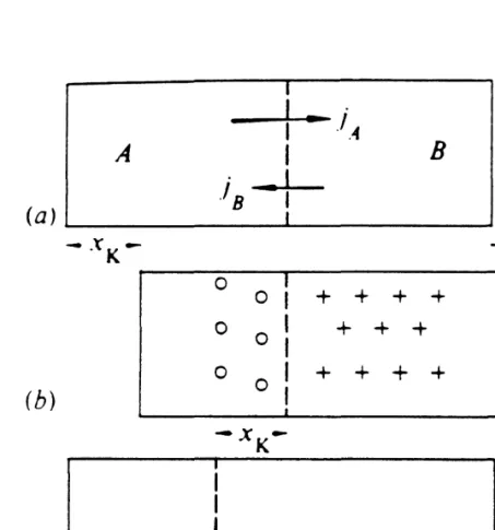
The simplest case of metal-metal interdiffusion occurring in a binary diffusion pair consists of single crystals of individual constituents, which upon interdiffusion form a continuous solid solution. Thus, the interdiffusion and reaction process can strongly depend on the morphology of the original diffusion.
Metastable Phases
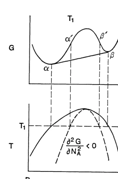
If we assume that this variation is small, the total free energy can be expanded in terms of the composition gradient. The change in the total free energy of the system, initially homogeneous with composition No. a when subjected to a sinusoidal fluctuation.
TEMPERATURE
- Solid State Amorphization
- Introduction to the Thesis
- References
- Introduction to Sputter Deposition
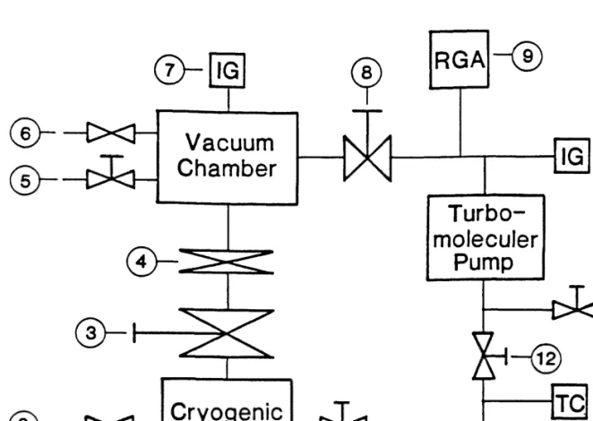
- Vacuum System
Using the Rutherford backscattering spectrometry (RBS) technique elucidated some important aspects of the growth kinetics of the amorphous NiZr interlayer. In Chapter 3 we will describe our study of the growth kinetics and thermodynamics of amorphous NiZr formation in sputter-deposited polycrystalline Ni/Zr multilayer diffusion pairs.
IG RGA √2)
Sputter Deposition: Operation and Monitoring
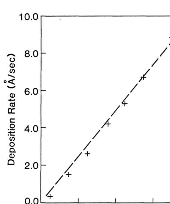
Sputtered material comes from the high plasma density areas, and the sputter erosion of the target also has an annular shape. The thickness distribution of the resulting thin film, condensed on the substrate, agrees with the calculated results, assuming a super. Calibration of the crystal oscillators is necessary because their positions do not coincide with the actual substrates.
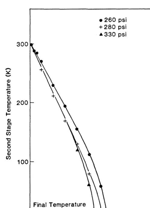
Over a 5-centimeter distance from the center of the sputter guns, the film thickness has been found to vary by no more than 5%. It should be emphasized that the residual gas content in the main chamber during sputtering is obtained by converting the sampled gas content in the differentially pumped spectrometer chamber without subtracting the background contribution (i.e. the residual gas content measured when the system is at its base). pressure). The results indicate that while the Ar pressure during sputtering is in the mTorr range, the partial pressure is off.
Thus, at first glance, the contamination of condensation thin films with reactive gas impurities at the lθ-o rporr level would reach 10 to 50% (assuming a sticking coefficient of unity) with typical pure metal deposition rates in the range of one to five monolayers per second. (3 to 15 Â/s). However, the rate of intrusion of reactive impurity gases onto the substrate surface is greatly reduced by the presence of Ar gas.
Summary
The overall free energy of the system can be reduced by interdiffusion of pure elements until the system consists of a single equilibrium crystalline phase or a combination of these phases according to equilibrium thermodynamics.
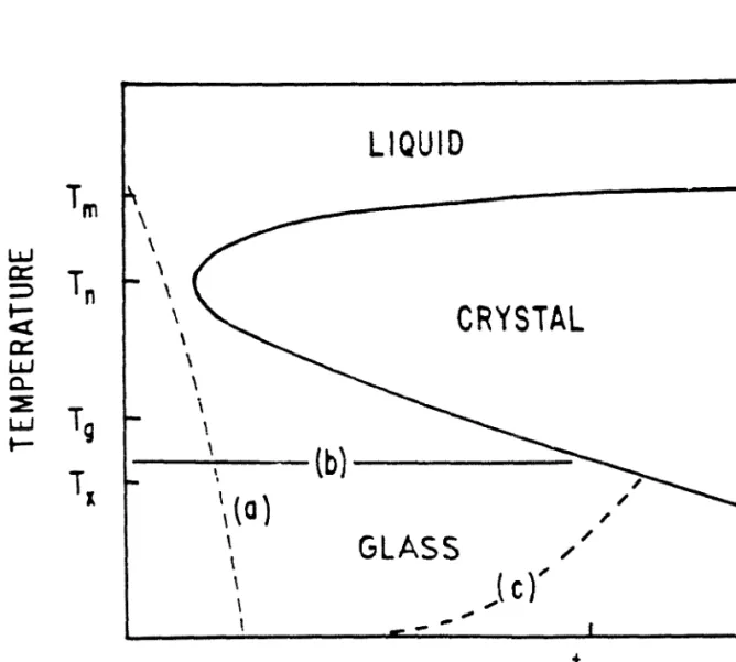
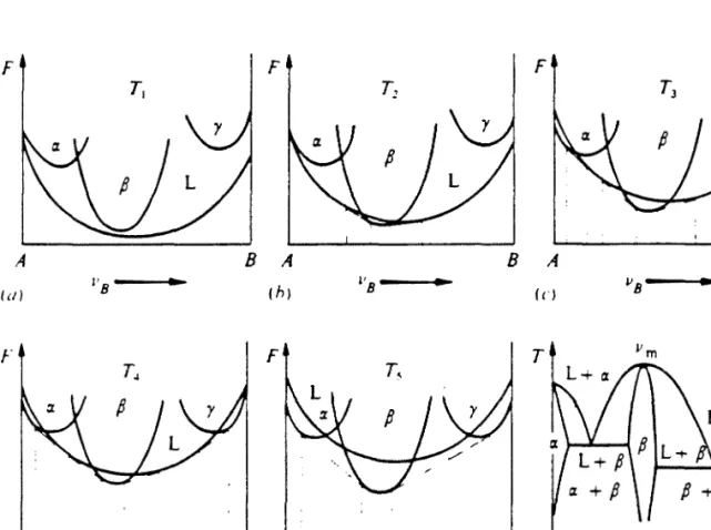
Equilibrium phase diagrams and free energy diagrams
A binary phase diagram can be derived if the dependence of the free energies of the terminal solid solutions and various compounds of tem. A knowledge of the free energy functions of all phases, stable or metastable, determines whether the formation of a particular phase is thermodynamically possible. Thermodynamic data for pure elements are available from which the free energies of pure elements can be calculated[3].
Experimentally determined equilibrium phase diagrams together with some thermodynamic models are often used to determine the free energy functions of equilibrium phases[4]. Amorphous alloys are usually modeled as an extension of the liquid state down to the supercooled regime. Direct measurement of thermodynamic data on metastable alloys including amorphous alloys is scarce at best.
Planar Growth Kinetics of a Single Compound Interlayer
Compound β is assumed to form and grow between two saturated phases a and ^∕ (eg the two saturated terminal solid solutions). The a∕β and β/^ interfaces move due to interdiffusion and the thickness of the β phase grows with time. Such a condition is implied in the concentration profile shown in Fig. 3.2 be depicted. Schematic illustration of growth of a single-junction interlayer in a planar binary diffusion pair.
The steady-state condition can be used to further simplify the situation, since under this assumption. The condition of interface quasi-equilibrium is implicitly assumed; i.e. the deviation from thermodynamic equilibrium at the interfaces is assumed to be small enough to justify a linear response of the interfaces to the degree of deviation from equilibrium. It is clear from equation (7) that there exists a characteristic length Xp = Dp∣Kβi in the growth of the β-composite interlayer such that the thickness of the β-interlayer is proportional either to the time t or to the square root of the time f1 ∕ 2, depending on whether the interlayer thickness is significantly below or above this characteristic length; i.e.,
Experimental determination of the growth kinetics of a single compound layer usually involves the determination of the thickness of the interlayer of the compound as a function. Such a phenomenological description of the interdiffusion process could fail within the limit of very small interlayer thicknesses [12].
Growth of the amorphous interlayer: X-ray and Resistivity Measure ments
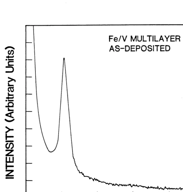
It can be seen that the sharp Bragg peaks of the deposited films are greatly reduced in intensity and a broad band has appeared indicating the presence of an amorphous phase. A rough measure of the growth kinetics of the amorphous NiZr alloy can be obtained from a detailed examination of the x-ray diffraction data. Because the amorphous NiZr alloy is the only new phase observed throughout the annealing process, its growth can be monitored by the consumption of Ni and Zr elements, which in turn is proportional to the decrease in the integrated peak intensity of X-rays of Ni and Zr. , assuming that no change in film texture occurs during the course of annealing[16].
The slight increase in the total intensity of the Ni peaks after the first 30-min annealing at 250 °C is most likely due to the recrystallization of some Ni crystallites. At both temperatures, the initial decrease in the total intensity of the Ni and Zr peaks is followed by a region of less rapid decrease. Furthermore, the annealing data at 250 °C show a break in the peak intensity curve between these two regions.
This fracture is the result of a smaller total scattering area due to the buckling of the substrate film. A similar effect is not observed in the case of annealing at 3150C because the film has already buckled.

NORMALIZEDINTENSITY
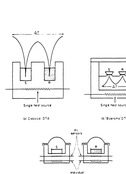
Differential Scanning Calorimetry
The sample to be examined is placed in one chamber, and a thermally inert reference material (such as AIq,Oq) with a similar heat capacity as the sample is placed in the other chamber. Both chambers are then heated identically by the oven at a constant heating rate, and the temperature difference between the sample and the reference material is detected by the temperature sensing equipment in each chamber and recorded as a function of the oven temperature. An average electronic control loop controls both the temperature of the sample and the reference material to follow a predetermined thermal history, and an additional control loop adjusts the current inputs to eliminate any detected temperature difference between the sample and the reference material.
The sample temperature is thus always kept the same as the reference temperature, and a signal proportional to the power difference between the power input to the sample and the reference material is recorded as a function of the temperature. The recorded signal at any time is proportional to the instantaneous rate of heat absorbed or released by the sample in the limit of small thermal resistance between the sample and the furnace[21]. The melting endotherm increases linearly on the leading edge due to the finite thermal resistance between the sample pan and the furnace[2l].
Melting points of various pure metals (e.g. In, Sn, Pb) can be determined and the instrument can be adjusted so that the measured melting points do not deviate from the table values by more than ±20C in the temperature range 50 - 600°C. After determining the calibration constant, the ordinate is immediately read in units of millicalories per second.
TEMPERATURE (K)
Summary
In this chapter, it was shown that the formation process of amorphous alloys in a thin film of vapor diffusion, both growth kinetics and ter. It has been proven that the lowering of the free energy during amorphization is of a chemical nature, arising mainly from the large negative heat during the mixing of elements to form an amorphous phase.
Chapter 4
- Specimen Preparation
- How Thick Can Amorphous Interlayers Grow?
- Is Nucleation Important?
- Models for Evolution of Diffusion Couples
- Summary
- References
In the relevant composition range, the heat of mixing of the amorphous phase averages around 30 kJ/mol. Additional annealing up to 18 h resulted in the formation of a NiZr compound instead of further growth of an amorphous NiZr interlayer, which is in agreement with other measurements [3]. The growth of the amorphous NiZr interlayer is limited by the formation of the NiZr compound.
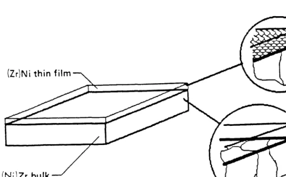
When a NiZr compound forms at the amorphous/Zr interface, the growth of the amorphous interlayer will stop. For sputter-deposited polycrystalline Ni/Zr diffusion pairs, an important observation is the lateral uniformity of the amorphous NiZr interlayer at an early stage of growth (see Fig. 2). Since grain boundaries are indeed present in our recrystallized Zr foil, we study their influence on the formation of the amorphous phase.
8 shows in plane view a bright field micrograph of the same poly-Ni/s-Zr diffusion pair after annealing. This micrograph shows that these residual low-energy Zr grain boundaries do not catalyze the formation of the amorphous phase. The condition for the continued growth of the amorphous interlayer can be simply stated as an inequality between these two time scales.
Since the growth of the amorphous interlayer is diffusion controlled, the amorphous/Zr interface velocity can be related to the thickness of the amorphous interlayer xam at.