Due to the nature of the devices being manufactured, all materials used must be extremely clean. The work that will be described in this dissertation continues in the direction of the latter set of techniques.
DIRECT MEASUREMENT OF ADHESIVE FORCES PERTINENT TO THE ALIGNMENT OF RANDOMLY DISPERSED MICROWIRES
Introduction
The self-assembly of nanoparticles has been well studied, with reports of the assembly of a variety of structures including face-centered cubic arrays and body-centered cubic arrays and hexagonal close-packed monolayers. 29–34 The spontaneous assembly of nanoparticles into ordered arrays is based on the small dimensions of the particles. Due to the extremely small size of the particles considered, the forces between the particles, which increase with surface area, can.
Background
When the cantilever is deflected, the laser beam moves onto the detector, which is then converted via calibration data into the upward or downward motion of the cantilever. Finally, given the spring constant of the cantilever, an application of Hooke's law fits the data for the cantilever deflection into the force felt by the tip of the cantilever as a function of probe position.
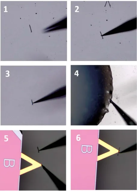
Tip Preparation
A separate micromanipulator tip was used to collect a small amount of epoxy and spread the adhesive onto the tip of the AFM cantilever. Once prepared, the effective spring constant of the adapted AFM probes was measured using cantilever calibration standards (Bruker CLFC-NOBO).
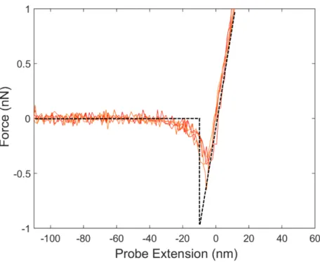
Adhesion Measurements
There is no visible adhesion between the microwire and the SiOH substrate in isopropanol, and any visible adhesion on the SiH surface is not clearly distinguishable from the background noise. From the magnetic alignment data alone, it can be concluded that the relative adhesion strengths are Si-H/water > SiH/isopropanol > SiOH/isopropanol > SiOH/water.

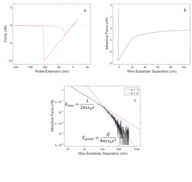
Coulombic Force Characterization
The functional form of the force versus separation can be better understood by plotting the data on a logarithmic scale. This corresponds to the length of the raised linear areas visible in the texture of the metal coating.
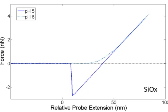
Manipulating Adhesion with Surface Charge
In the following experiments, a nickel-coated wire was used as the AFM tip and a piece of gold-coated silicon wafer was used as the substrate. The dashed blue line shows dramatically different behavior in the presence of the redox couple.
Conclusions
THE INFLUENCE OF SUBSTRATE TEXTURE ON MORPHOLOGY OF SELF-STRUCTURING PHOTOELECTRODEPOSITED
SEMICONDUCTOR FILMS
Introduction
Background
The postulated explanation was that dipole scatterers randomly placed on the surface scattered the light in the plane of the electrode surface. However, the illumination used for a deposition is only a fraction of the light scattering that occurs on the surface of the photoelectrodes.
Ordered Growth on Abraded Electrodes
The intensity was tuned to 25 mW∙cm-2 by adjusting the lamp and polarizer positions. It was noted that, while most of the surface exhibited the type of morphology seen in previous studies, there were many isolated areas of abnormally straight lamellar growth. In addition to being morphologically distinct from the surrounding area, the orientation of the straight lamella often differed from the orientation of the rest of the film lamella.
Instead of growing along the direction of polarization of the light, the straight lamellae would often grow several degrees rotated from the expected direction, although no large areas of straight growth offset more than 15° from the direction of polarization were observed. The lamella on one side of the feature will briefly grow at a different angle to the feature before returning to the normal direction of growth on the other side of the feature. The random orientation of the straight domains and their presence only on surfaces that have a deformable top layer informed the hypothesis that the ordered domains were a consequence of scratches made inadvertently during the electrode fabrication process.
Since the GaIn eutectic was scratched into the back of the electrodes, the surfaces of the electrodes may have been worn by the cleanroom wipes (Texwipe, TX624) they were placed on.

Simulated Growth
The growth on top of the ridge also divides and spreads outward into the space nearby. This is probably caused by the strong absorption at the edges of the ridge that directs the growth to the corners and sidewalls of the ridge. This can be attributed to the increased straightness of the lamella adjacent to the ridge as opposed to the control lamella.
Instead of having randomly placed diffusers, the lamellas adjacent to the ridges have other lamellas adjacent to the ridge as a source of light that is diffused from the side opposite the ridge. However, as seen in the previous simulation, the growth converges to a structure that depends on the initial geometry of the substrate. The final simulation in this set has twice the ridge density of the previous example.
In this simulation, as before, the final pitch of the slat is not the expected pitch.
Lithographically patterned substrates
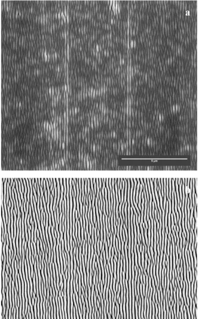
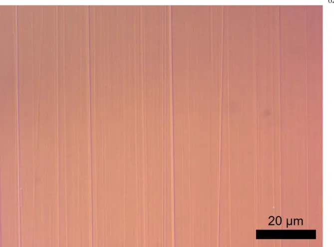
The grooves in the substrate were aligned with the edge of the electrode body to which the substrates were attached, and the polarizer was aligned so that the polarization direction aligned with the long dimension of the grooves. SEMs of the resulting morphology agree well with the simulated structure near the step edge. For the short depositions of 75 seconds, the lamellae immediately adjacent to the edges are much more clearly visible than the lamellae in the flat part of the electrode.
After 150 seconds of growth, the rest of the surface appears to have effectively caught up with the lamellae immediately adjacent to the surface discontinuity. The secondary growths are much better ordered in the SEM taken of the structured electrode. Nodules at the edge of the step are very well arranged on both sides of the step.
On the bottom, etched surface, pattern fidelity remains excellent up to several microns away from the surface pitch.
Abraded Substrates
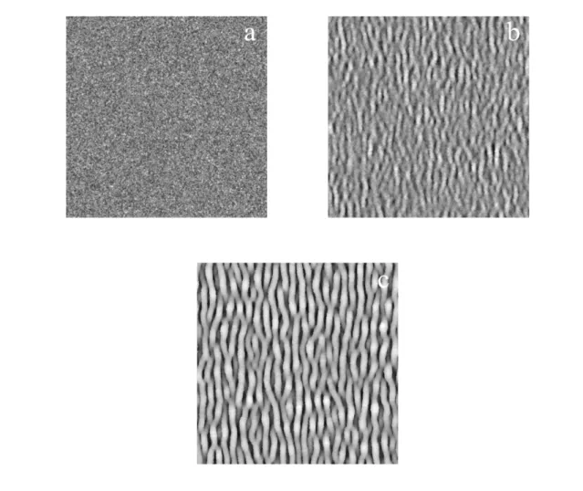
The polarization direction of the light was set to be parallel to the scratch direction. The vertical spots in the Fourier transform correspond to the periodicity of the knots growing on the lamellae. In the case of the control sample, the lamellae grow roughly in line with the direction of polarization of the light, but they meander back and forth across the electrode.
The Fourier transform of the SEM is similar to that of the green control sample. The lamellae are well separated, with a larger void space visible than in the SEM of the weathered sample illuminated with 532 nm light. The intensity peaks at the same locations relative to the center of the image as the maximum intensity in the transformed control image.
The wide variation in the spacing between lamellae is the result of the very different scratch widths in the sanded surface.
Conclusions
STRUCTURAL COLORATION OF SELF-STRUCTURED PHOTOELECTRODEPOSITED SEMICONDUCTING FILMS
Introduction
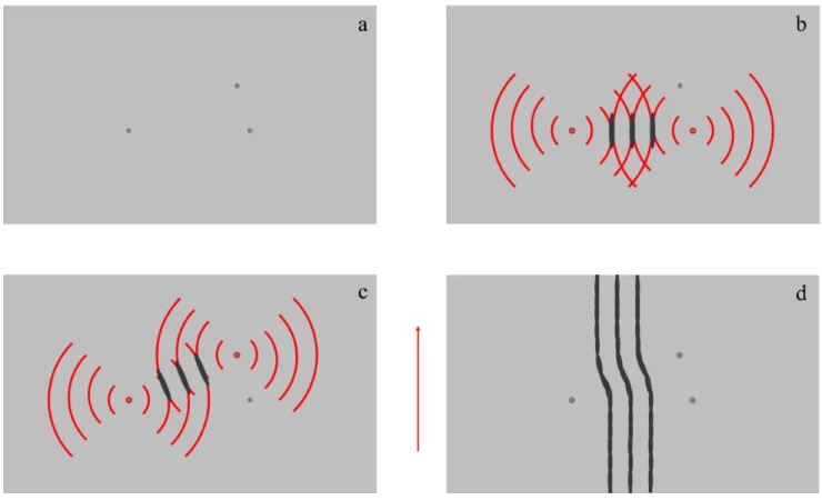
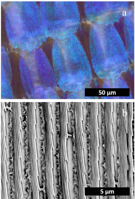
The morphology of these structures can also be modified using the previously discussed techniques if one wishes to adjust the properties of the resulting film. The two beams interfere and produce a series of intensity fringes across the illuminated surface.79 This variation in intensity across the surface causes only specific areas of the photoresist to be exposed. When viewed in a scanning electron microscope, ridges running along the long axis of the scale become apparent.
For electrolyte-deposited lamellae, this diffraction is most apparent when viewing the electrodes in the plane containing the vector perpendicular to the electrode surface and the polarization axis of the light source used for deposition. In other words, the staining is strongest when you tilt the sample in the direction of growth of the lamellae, rather than tilting the sample so that you are effectively looking over the tops of the lamellae. This suggests that there are periodic structures along the length of the lamellae that give rise to diffraction.
The conditions that produce the most iridescent samples also produce the samples with the most prominent nodular growth along the lengths of the lamellae.
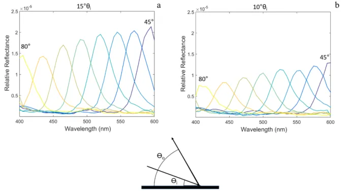
Diffraction Characterization
However, the qualitative agreement with theory confirms that the physical origin of the non-specular light from the surface is due to diffraction from the surface texture. To improve the reflectivity of the surface, a thin aluminum layer was applied to the textured surface. Neither the peak positions nor the line widths changed appreciably after aluminum deposition.
Disruption of the electrode surface and substrate light absorption probably reduced the light intensity in the second-order peak below the detection limit of the ellipsometer. Furthermore, the fraction of the total intensity that was deflected in the detector in the previous measurements is very small, even when the sample had a reflective coating, suggesting that the neglected intensity must come from the plane of the detector. The screen was placed 30 cm in front of the sample, which was mounted on a rotary stage.
The bright rectangular spot is from the specular reflection from the electrode surface.
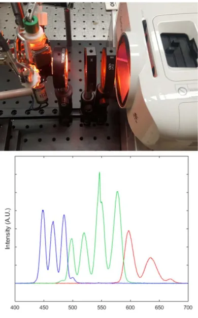
Manipulating Structural Coloration
An electrochemical cell was positioned so that the light from the projector would focus on the surface of an electrode in the cell, and a wire mesh polarizer was mounted in the path of the beam. Nitrocellulose based nail polish was used to seal the sides of the electrode and block any exposed metal on the electrode support. The "C" portion of the electrode was slightly darker, possibly due to more light being diffracted and less light undergoing specular reflection.
Under SEM, the rise of lamellae differed in the regions grown under red illumination versus regions illuminated with blue light during deposition. The C portion of the aluminized electrode had a slightly greener cast than seen in the bare sample. The wavelength of the light diffracted back to the camera continuously changed from red to blue as the sample was rotated.
The "C" portion of the electrode, which has a smaller period than the background, showed only deep purple color for the same reason.
Conclusions
BIBLIOGRAPHY
Comparison of the performance of CoP-coated and Pt-coated radial junction n+p silicone microwire array photocathodes for the sunlight-driven reduction of water to H2(g). The physics of polyprotein pulling: a review of single-molecule force spectroscopy using the AFM to study protein unfolding. The standard oxidation potential of the ferrocyanide-ferricyanide electrode at 25° and the entropy of ferrocyanide ions.
Porous silicon and alumina as chemically reactive templates for the synthesis of SnSe, Sn and SnO2 tubes and wires. Self-Optimization of Photoelectrochemical Growth of Nanopatterned Se-Te Films in Response to Spectral Distribution of Incident Illumination. Morphological expression of coherence and relative phase of optical inputs in photoelectrodeposition of nanopatterned Se-Te films.
Polarization control of morphological pattern orientation during light-mediated synthesis of nanostructured Se–Te films.