Engineering Organic and Perovskite based Solar Cells
A dissertation submitted in partial fulfilment of requirements for the degree of Doctor of Philosophy
by
Ritesh Kant Gupta Roll No. 166153004
Centre for Nanotechnology
Indian Institute of Technology Guwahati Guwahati-781039, Assam, India
September 2021
TH-2676_166153004
TH-2676_166153004
I do hereby declare that the work incorporated in this thesis entitled, “Engineering Organic and Perovskite based Solar Cells” is the result of investigations carried out by me under the guidance of Prof. Parameswar Krishnan Iyer, at the Centre for Nanotechnology, Indian Institute of Technology Guwahati, Guwahati, Assam, India.
In keeping with the general practice of reporting scientific observations, due acknowledgements have been made wherever the work described is based on the findings of other investigators. I further declare that this work has not been submitted in part or full to any other university or institute for award of any degree or diploma.
IIT Guwahati Ritesh Kant Gupta
September 2021
TH-2676_166153004
TH-2676_166153004
Dr. Parameswar K. Iyer
Professor, Department of Chemistry and Center for Nanotechnology
Indian Institute of Technology Guwahati Guwahati-781039, Assam, India
http://www.iitg.ac.in/chemistry/fac/pki/
Phone : +91-361-2582314 Fax : +91-361-2690762 :+91-361-2582349 E-mail: [email protected]
Certificate
This is to certify that the work included in this thesis entitled “Engineering Organic and Perovskite based Solar Cells” by Mr. Ritesh Kant Gupta, Centre for Nanotechnology, Indian Institute of Technology Guwahati has been carried out under my supervision. I further certify that this work has not been submitted to any other University or Institution in part or full for the award of any degree or diploma.
Place: IIT Guwahati Parameswar Krishnan Iyer
Date: 28 September 2021 Thesis supervisor
Department of Chemistry
Indian Institute of Technology Guwahati Guwahati – 781039, Assam, India
TH-2676_166153004
TH-2676_166153004
Dedicated to my teachers
TH-2676_166153004
TH-2676_166153004
Table of Contents
Acknowledgement i
Thesis Abstract v
List of Figures vii
List of Tables x
Chapter 1: Introduction 1
Abstract 3
1.1 Overview 4
1.2 History of Solar Cells 5
1.3 Parameters to Define Solar Cell Performance 6
1.4 Generations of Solar Cell 8
1.5 Organic Solar Cell 11
1.6 Perovskite Solar Cell 16
1.7 Thesis Synopsis 22
References 25
Chapter 2: Regulating Active Layer Thickness and Morphology for High
Performance Hot-casted Organic Solar Cells 31
Abstract 33
2.1 Overview 34
2.2 Experimental Section 35
2.3 Results and Discussions 36
2.4 Conclusions 45
References 46
Chapter 3: Halide Engineering for Mitigating Ion Migration and Defect
States in Hot-casted Perovskite Solar Cells 49
Abstract 51
3.1 Overview 52
3.2 Experimental Section 54
3.3 Results and Discussions 55
3.4 Conclusions 68
TH-2676_166153004
References 69 Chapter 4: Ambient Stable Perovskite Solar Cell through Trifluoro
Acetic Acid-mediated Multifunctional Anchoring 71
Abstract 73
4.1 Overview 74
4.2 Experimental Section 75
4.3 Results and Discussions 77
4.4 Conclusions 86
References 87
Chapter 5: Dual-Passivation Strategy for Improved Ambient Stability of
Perovskite Solar Cells 91
Abstract 93
5.1 Overview 94
5.2 Experimental Section 96
5.3 Results and Discussions 97
5.4 Conclusions 108
References 110
Chapter 6: Summary and Prospects 113
6.1 Summary 115
6.2 Prospects 116
Outcomes 119
Conferences & Workshops 122
TH-2676_166153004
i
I am delighted to put across my heartfelt appreciation and gratefulness to everyone who in one way or the other have contributed in the completion of this thesis. Many individuals have supported me in this truly unforgettable and amazing journey. I have tried to list everyone who have sincerely helped and guided me in the completion of this thesis. I thank each person from the bottom of my heart.
First of all, I am extremely beholden to my supervisor and mentor Prof. Parameswar Krishnan Iyer for providing me a precious opportunity to work in his group. His continuous support, valuable suggestions, scientific guidance, deep insights, and motivation have encouraged me to take up the tasks and introduced me to a field that I knew little about. I earnestly thank him for having trust in me and giving me total freedom in choosing the direction of my research. I feel fortunate to have him as my guide who has always motivated me with his hard work, dedication and optimism. He has been ever patient with me and was always available to provide his very useful opinion regarding my thesis work.
Besides my supervisor, I am highly indebted to my doctoral committee members, Dr.
Partho Sarathi Gooh Pattader, Prof. Perumal Alagarsamy, Dr. Kalyan Raidongia and Dr.
Uday Narayan Maiti for assessing my research work regularly. Their invaluable suggestions and crucial comments during all my seminars helped me broaden my research from various perspectives and improve my thesis.
My sincere thanks also goes to Dr. Arun Tej M., Department of EEE, IIT Guwahati. I found him available whenever I was having a query related to the charge transport kinetics of any electronic devices. Also, timely advices and remarks from Prof. Mohammad Qureshi, Department of Chemistry, IIT Guwahati, on the experiment techniques were very useful in understanding them better.
I sincerely express my gratitude towards all my teachers especially Mrs Sumita Pal (Miss), Mrs Arpita Majumder (Didi), Mr. Kalyan Ashish Khan (Bhaiya), Mr. Kalyan Sinha Roy, Mr. Amitava Chatterjee, Dr. Devmalya Banerjee and Dr. Hirok Chaudhuri for imbibing good values and knowledge in me.
TH-2676_166153004
ii
I am also thankful to all the research scholars and staff of the Centre for Nanotechnology, IIT Guwahati for their kind cooperation and support. Further, I am grateful to Department of Chemistry and Central Instrument Facility, IIT Guwahati for allowing me to access their facility for the various experimentations as and when required. I am indebted to the staff of Student Affairs, Academic Affairs and Finance sections of IIT Guwahati for being kind enough to advise and help in their respective roles. I also appreciate the efforts of Pathak Ji, Core 1 Xerox Centre, and his staff, Haloi Da and Gautam Da, for their endless help during my stay at IIT Guwahati.
I had the best of the times working with Adil Bhaiya and Rabi who were my core solar team members. Both of them deserve the best and utmost respect for their hard work, diligence and indispensable input into the overall research work. Also, I learnt a lot from Ashish Bhaiya and Radha Bhaiya regarding various aspects of organic solar cells during my earlier days at IIT Guwahati. Further, the research experience gathered along with Anwesha, Ramesh Bhaiya and Maimur Da is also worth mentioning.
I would also like to acknowledge all my other lab mates including Sameer Bhaiya, Suresh Bhaiya, Priyanka Mam, Dip Bhaiya, Anamika Dey Madam, Gopi Bhaiya, Sayan Da, Arvin Bhaiya, Rahul Bhaiya, Raman Bhaiya, Nehal, Paromita, Retwik, Biki, Raj, Priyam, Debika, Dibash, Mayur, and Geetmani Da for their timely assistance and support. I also had a great learning experience with Sahu Sir, Bikoshita, Priyanka and Swapna while they completed their summer internship project with me. I would also like to thank each one of them for creating a pleasant laboratory atmosphere and making my days memorable.
I was privileged to be part of the organizing team of ICANN2017 and ICANN2019 conferences. I had the opportunity to interact with the topmost scientists across the world and discuss my research work with them. I am extremely appreciative for the valuable inputs received from Prof. Han Young Woo, Korea University, Prof. Shyam Pandey, Kyushu Institute of Technology and Dr. Ankur Solanki, Pandit Deendayal Energy University.
I was also fortunate to be working in the Organic Electronics Laboratory of IIT Guwahati which houses all the sophisticated instruments. I have learnt a lot to keep these instruments in working conditions through proper maintenance. During all the maintenance activities, I have received ample support from various engineers. I would like to thank Mr. R.
TH-2676_166153004
iii
K. Tripathi, RVL Scientific & Engineering Pvt. Ltd., Mr. T. P. Kundu, IKA India Pvt. Ltd., Mr. Subrata Sardar, Silsil International Pvt. Ltd. and Mr. M. Nandan, Bat-Sol Equipments &
Technology. They have extended all possible help as and when required. Further, I am also grateful to Dr. Prasad Gosavi and Mr. Rajkumar Somendrajit Singh, Anton Paar India Pvt.
Ltd. for helping me with the GIWAX measurements in the organic solar cell work.
I extend my sincere thanks to my cycling group comprising of Rahul Bhaiya, Nilanjan Da and Anwesha. All our weekend cycling trips will be one of the most memorable times that I will be taking back from IIT Guwahati. I am genuinely gratified to the moments spent with Nystha, Nirmal, Rabi, Atanu and Himangshu. All the discussions beyond work with all these friends helped me focus more on the research.
Also, I would like to thank my friends Ritwik, Kaka, Navadeep Bhai, Vivek Bhai, Suresh, Anish, and Hrishi from NIT Durgapur. All of them helped me understand the true sense of joining as a PhD student at IIT Guwahati after Masters.
Further, I acknowledge Debdipta, Sayantan, Vivek, Ankit, Aakash, Prateek and Sarbojit from the bottom of my heart. Thank you guys for helping me right from the beginning of knowing each other and provide all the moral support time and again.
Finally, I would like to express admiration towards my go to person, Sankalpita, who has spent endless number of days wishing for the bests of the world for me. I believe this is the best I could have done for her – complete a PhD. At the end, I want to thank my parents, brother and sister-in-law for their prayers, sacrifice and struggle. It is because of them I am able to live my dream and complete my higher education from a prestigious institute. They have always given me the strength to chase my dreams which was immensely needed.
I express gratitude towards each individual for extending their support, encouragement and remembering me in their prayers.
Ritesh Kant Gupta
TH-2676_166153004
[This page was intentionally left blank]
TH-2676_166153004
v
It has become utmost necessary to address the energy crisis and reduce the carbon emission simultaneously. Therefore, exploration of various renewable energy sources is now the need of the hour. Among all the renewable energy sources, solar energy is considered to be the most sustainable owing to its ample availability on the surface of earth. The first and second generations of solar cell has been already commercialized and is being utilized to reduce the load on the current method of energy production through fossil fuels. However, to further consolidate the efforts, commercial utilization of the third and fourth generations of solution processable solar cells are also important. The organic solar cell (OSC) and perovskite solar cell (PSC) are the front runners among all the solution processed photovoltaic technology owing to its various advantages and PCE reaching beyond 18% and 25% respectively. Further, both these solar cells offers ease of fabrication with low-cost and abundant materials ensuring that they can be significant contributor to commercial photovoltaic technology in the near future.
This thesis is broadly organized into two parts. The first part (comprising of one chapter) and second part (comprising of three chapters) focuses on fabrication of OSC and PSC, respectively. Two techniques have been employed in this thesis work for the fabrication of solar cells: (i) hot-casting technique in the first two working chapters, and (ii) room temperature anti-solvent method in the remaining two working chapters. At first, hot-casting technique is used to develop OSC through regulation of morphology and thickness. Highest power conversion efficiency (PCE) of 9.13% was obtained for a thick active layer film.
Thereafter, hot-casting technique is again implemented to fabricated mixed-halide PSC by varying the ration of methyl ammonium bromide in the precursor solution. The modified PSC resulted in PCE of 18.08% which also displayed large micrometer sized grain and reduced nanometer sized grain boundaries to minimize the recombination of the photo- generated charges. Further, trifluoro acetic acid is used as additive in perovskite solution to regulate the crystallization, minimize ion migration and charge recombination in PSC. As a result, champion 20.10% PCE was obtained in the modified device. Finally, p-toluene sulphonic acid is utilized to control the crystallization kinetics of the perovskite bulk and also passivate the traps. Simultaneously, polystyrene is used to increase the moisture resistance
TH-2676_166153004
vi
and reduce the surface defects of the perovskite films. This dual-passivation strategy resulted in champion PCE of 20.62% with superior ambient stability.
The efforts made in this thesis highlights the usefulness of various device engineering to develop OSCs and PSCs to regulate the morphology and crystallization of the photo-active layer to achieve highly efficient, stable and repeatable solar cells. The thesis provides the basis for facilitating the commercialization of OSC and PSC in the near future.
TH-2676_166153004
vii
List•of•Figures•
Figure! Caption! Page!
1.1 A typical example of (a) J-V curve and (b) power output versus voltage
curve recorded under light illumination 6
1.2 A typical EQE spectrum of a perovskite solar cell 8
1.3 Classification of four generations of solar cell 9
1.4 Working principle of organic solar cell 13
1.5 OSC device architecture (a) conventional, and (b) inverted 13 1.6 Most commonly used donor acceptor materials for OSC 14 1.7 Scheme of perovskite crystal unit cell (a) A-cation centered and (b) B-
cation centered 17
1.8 Working principle of perovskite solar cell 18
1.9 PSC device architecture (a) mesoscopic, (b) planar conventional and (c)
planar inverted 18
1.10 Commonly used organic passivating molecules used in PSC 21
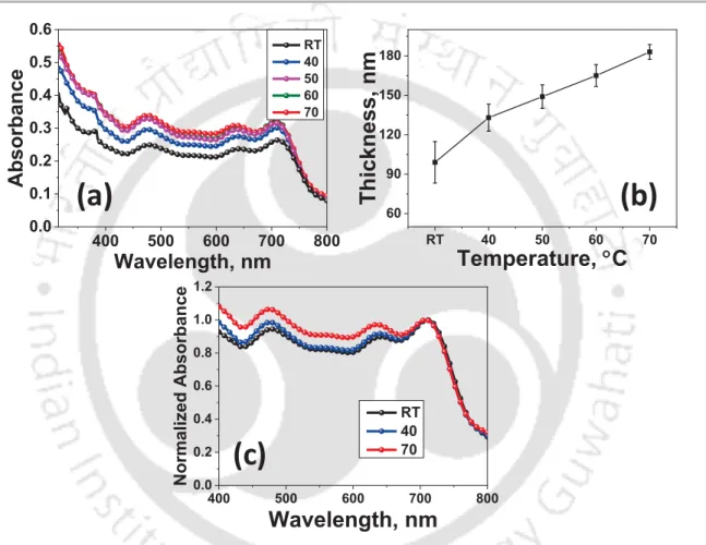
2.1
(a) Absorbance of blend films coated at various temperatures, (b) variation of active layer thickness with hot-casted temperature and (c) normalized absorption to show decreased crystallinity and increased fullerene loading
37
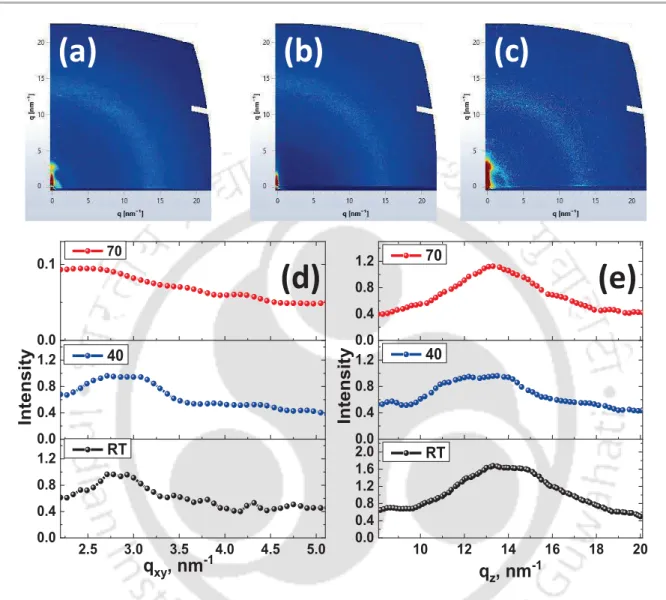
2.2 2D GIWAX images of films for (a) RT, (b) 40 °C, (c) 70 °C, 1D GIXRD
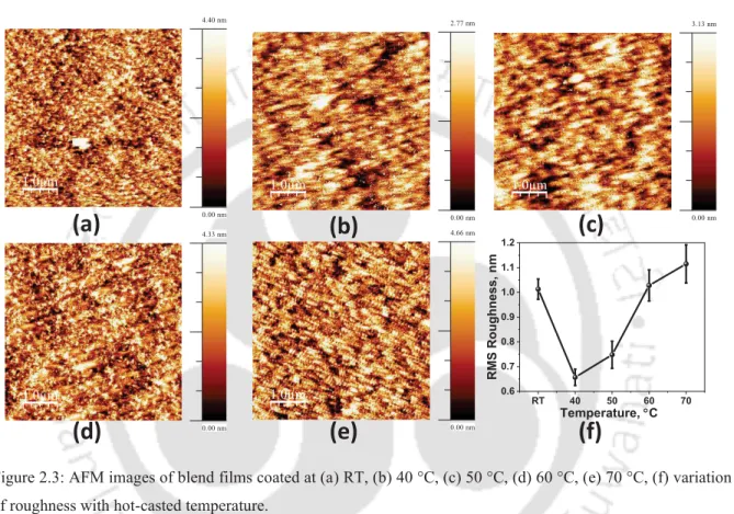
profile of films (d) in plane and (e) out of plane 38 2.3 AFM images of blend films coated at (a) RT, (b) 40 °C, (c) 50 °C, (d) 60
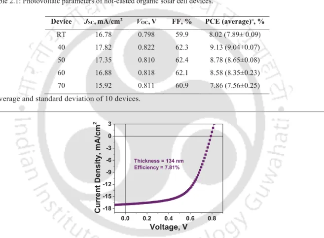
°C, (e) 70 °C, (f) variation of roughness with hot-casted temperature 39 2.4 Schematic diagram showing the device fabrication steps 40 2.5 (a) J-V graph of the fabricated devices, (b) corresponding EQE 40 2.6 J-V characteristic curve of device fabricated with 134 nm active layer at
RT 41
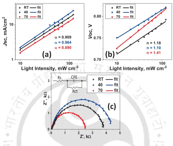
2.7 Box chart showing variation of (a) PCE, (b) Jsc, (c) Voc, and (d) FF 42 2.8 (a) Jsc versus light intensity plot, (b) Voc versus light intensity plot, (c)
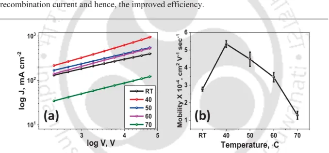
Impedance spectra and the fitting circuit in inset 43 2.9 (a) SCLC plot for hole only devices, and (b) variation of mobility with
hot-casted temperature 44
TH-2676_166153004
viii
Figure! Caption! Page!
3.1
(a) XRD patterns of perovskite films with various MABr concentrations, (b) Enlarged XRD patterns to evaluate the peak shifting, (c) UV-vis absorption spectra of perovskite films with different MABr
concentrations, (d) Tauc plot, and (e) PL curve of perovskite films with different MABr concentrations
56
3.2
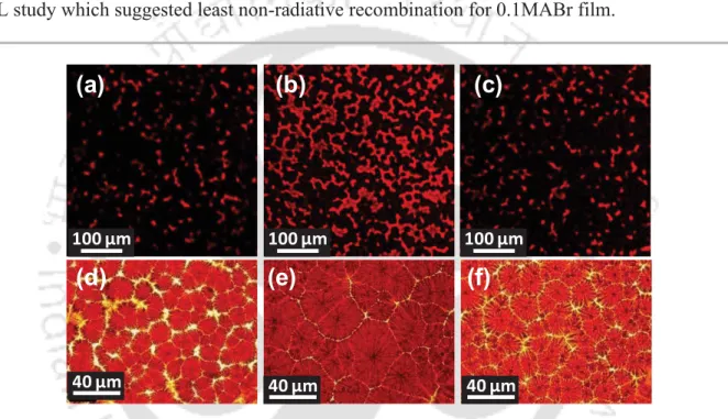
Confocal intensity mapping of the perovskite films for (a) control, (b) 0.1MABr, and (c) 0.2MABr; optical microscopic images of the perovskite films for (d) control, (e) 0.1MABr, and (f) 0.2MABr
57
3.3
Histogram plot showing grain size variation of perovskite films for (a) control, (b) 0.1MABr, and (c) 0.2MABr obtained from the microscopic images
58
3.4
FESEM images of the perovskite films for (a) control, (b) 0.1MABr, and (c) 0.2MABr; AFM images of the perovskite films for (d) control, (e) 0.1MABr, and (f) 0.2MABr
58
3.5
Line profile along the grain boundaries to measure grain boundary width for (a) control, (b) 0.1MABr, and (c) 0.2MABr obtained from the AFM images
59 3.6 Device fabrication steps of the hot-casted perovskite solar cells 60 3.7
J–V curves of the devices with various MABr concentrations, (b) EQE curves of devices with integrated Jsc spectra, and (c) steady-state current measured at the maximum power point for the 0.1MABr device
61 3.8 Box chart showing variation of (a) PCE, (b) Jsc, (c) Voc, and (d) FF! 62 3.9
Hysteresis analysis of the perovskite devices for (a) control, (b) 0.1MABr,
& (c) 0.2MABr, and Dark J-V analysis of hole-only perovskite devices for (d) control, (e) 0.1MABr, & (f) 0.2MABr
63 3.10 (a) Nyquist plots of the devices with various MABr ratios, (b) ln(•) vs
photon energy plot used to estimate Urbach energy, and (c) MS plots 64 3.11
(a) Dark J-V curves of the solar cell devices with various MABr ratios, and (b) Jph vs Veff characteristics with double logarithmic axis for different MABr ratios
65
3.12
(a) Normalized efficiency of control and 0.1MABr devices stored at room temperature in a relative humidity of 40 ± 5%, (b) XRD patterns of perovskite films showing stability after 20 days, and (c) Enlarged XRD patterns to evaluate no peak shifting
66
3.13 Forward and reverse J–V curves of control and 0.1MABr large-area
devices 67
4.1
(a) Chemical structure and ESP profile of TFAA, (b) FTIR spectra of TFAA, Control and TFAA+Perovskite, FESEM images of (c) control, (d) 1TFAA, (e) 2TFAA, (f) 3TFAA, and (g) XRD of all perovskite films
77 4.2 Steps of perovskite solar cell device fabrication with and without TFAA 78 4.3 (a) J-V graphs of the best devices of each type, and (b) EQE and
Integrated Jsc spectra of control and 2TFAA 79
TH-2676_166153004
ix
Figure! Caption! Page!
4.4 Box chart presenting device parameters variation for 15 devices of each
type (a) PCE, (b) Jsc, (c) Voc, and (d) FF 80
4.5 (a) J-V graph of 2AA, (b) FESEM image of 2AA, and (c) Box chart for
comparing the results of 2AA with control & 2TFAA 81 4.6 (a) Hysteresis study of control and 2TFAA, and (b) Steady state analysis
of control and 2TFAA 81
4.7 (a) UV-absorption profile, (b) ln(A) versus energy plot, (c) Tauc plot, and
(d) Steady state PL 82
4.8 a) Voc versus light intensity plot, and (b) Jsc versus light intensity plot 83 4.9 (a) EIS spectra, (b) Dark J-V graphs, (c) Jph versus Veff plots and (d) Mott-
Schottky plot 84
4.10 (a) Ambient stability study of the control and 2TFAA device, (b) Contact
angles, and (c) XRD of the perovskite films kept in ambient condition 85 5.1
(a) Schematic representation of dual-passivation coating, FESEM images (scale bar = 500 nm) of (b) control, (c) PTSA1PS2, (d) PTSA1PS4, (e) PTSA2PS2, (f) PTSA2PS4, (g) PTSA3PS2, (h) PTSA3PS4, and (i) XRD patterns of all perovskite films
98
5.2 Electro-static profile of PTSA 98
5.3 Box chart showing variation in (a) PCE, (b) Jsc, (c) Voc, and (d) FF for
15 devices of each type 99
5.4 J–V curves of the (a) dual-passivated & control devices, and (b) only
PTSA and only PS passivated devices 100
5.5 (a) UV-vis absorbance, and (b) Tauc plot! 101
5.6
(a) Hysteresis study of control and PTSA2PS2 device, (b) EQE and integrated Jsc spectra of control and PTSA2PS2, (c) Steady state analysis of control and PTSA2PS2, and (d) J-V of large-area PTSA2PS2 device
102 5.7 a) Impedance Spectroscopy, and (b) Mott-Schottky analysis 103 5.8 (a) Recombination resistance versus voltage plot (b) Capacitance versus
voltage plot, and (c) Trap DOS versus energy level plot 103 5.9 (a) Dark J-V plots of the solar cell devices, and (b) Jph versus Veff plot 104 5.10 (a) Dark J-V curve of hole-only device, (b) ln(A) versus energy plot to
estimate Urbach energy, and (c) PL spectra of the perovskite films 105 5.11 (a) Jsc variation with light intensity, and (b) Voc variation with light
intensity 106
5.12 (a) Contact angle measurement, Normalized device parameters variation
when put through ambient stability (b) PCE, (c) Jsc, (d) Voc, and (e) FF 107 5.13 XRD patterns of the perovskite films to check ambient stability 108
• •
TH-2676_166153004
xi
List•of•Tables•
Figure! Caption! Page!
2.1 Photovoltaic parameters of hot-casted organic solar cell devices 41 3.1 Photovoltaic parameters of small area hot-casted solar cell PSC devices 61 3.2 Photovoltaic parameters of large area hot-casted solar cell PSC devices 67
4.1 Photovoltaic parameters of the fabricated devices 80
5.1 Device/Film type based of the concentration of PTSA and PS for dual
passivation strategy 95
5.2 Photovoltaic parameters of all types of fabricated using dual-passivation
approach 100
• •
TH-2676_166153004
Chapter•1
Introduction
Engineering!Solar!Cells
Organic!Solar!Cell (Third!Generation)
Perovskite!Solar!Cell (Fourth!Generation)
/ /
TH-2676_166153004
Chapter!1!!!!!!!!!!!!!!!!!!!!!!!!!!!!!!!!!!!!!!!!!!!!!!!!!!!!!!!!!!!!!!!!!!!!!!!!!!!!!!!!!!!!!!!!!!!!!!!!!!!!!!!!!!!!!!Introduction!!
2
[This page was intentionally left blank]
•
TH-2676_166153004
Introduction Chapter!1!
3 Abstract•
Today, electricity is one of the basic necessities of human beings. It is required for our entire daily needs such as lighting, entertainment, cooking food, etc. Even electricity is an indispensable necessity for improved standard of living demands development through setting up of new industries and modern transport facilities. However, most of the electricity produced these days is through fossil fuels which are limited and creates lots of pollution resulting in many cities turning inhabitable. Thus, there is an urgent need to increase the use of clean, renewable and sustainable energy sources such as solar, wind, tidal, etc. for electricity generation. Solar energy has become one of the most promising sources of energy for production of electricity and has attracted various research groups for its exploration in various ways. In this introduction chapter, the importance of solar energy exploration has been discussed. Thereafter, the history of the development of solar cells including the four generations of solar cells is covered. The various parameters to define the efficacy of any solar cells device has been explained briefly. Then, the development of organic solar cell and perovskite solar cell, which are the main focus of this thesis, has been reported. The working principle, different device architectures and various engineering aspects to improve the device performance has been discussed elaborately for few types of photovoltaic devices.
Lastly, the chapter ends with a synopsis of the thesis.
•
TH-2676_166153004
Chapter!1!!!!!!!!!!!!!!!!!!!!!!!!!!!!!!!!!!!!!!!!!!!!!!!!!!!!!!!!!!!!!!!!!!!!!!!!!!!!!!!!!!!!!!!!!!!!!!!!!!!!!!!!!!!!!!Introduction!!
4
1.1•Overview•
With the enhancement in per capita income and lifestyle, energy sector has seen tremendous growth owing to its increasing global demand at 1.8% per annum. It is expected that, by the end of next decade, approximately 20 TW of energy would be required to fulfill all industrial, commercial, agricultural, transportation and domestic usages.1 Currently, fossil fuels such as coal, oil and natural gas are the sources for majority of the energy production across the world. All these sources are non-renewable in nature and the increasing consumption will lead to shortage of these sources which in turn would increase the cost per unit of the energy consumption. Also, fossil fuels offer a major disadvantage by contributing to greenhouse gases which are leading to global warming and air pollution.2 The most harmful for the environment is the energy production from coal because it has many more harmful combustion products than other sources of fossil fuels.3, 4 Another disadvantage is extraction of these fossil fuels which causes accidents and loss of human life.5 Currently, India is fourth in energy consumption among all countries behind Russia, United States of America and China.6 Like all other nations which are thriving to improve its standard of living, India also depends on fossil fuels for more than 90% for its electricity generation.7 As per a recent report in 2021, India consists of 22 polluted cities among the top 30 polluted cities in the world and most of them because of very poor air quality index.8 This calls for a paradigm shift for the energy production technology towards renewable sources such geothermal, nuclear energy, wind, biomass and solar energy which can lead all renewable energy sources in electricity generation.
Solar energy is one of the best alternate sources of energy to power the earth. With its renewable nature and approximately 89000 TW striking the surface of the earth every year, the 20 TW projected energy requirements can be fulfilled by installing solar panels in
~0.02% area of the earth.1 To give it a pictorial view, solar panels with area as large as Benin (a small country in Africa) or Greece will be sufficient to power all energy requirements of the world ten years later. With respect to Indian perspective, solar panels of the land area of the state of Telangana or Tamil Nadu or half of Rajasthan will be adequate to energize the world a decade later. Many countries have come together and agreed upon addressing the issue through increasing the usage of solar energy to minimize the pollution and global
TH-2676_166153004
Introduction Chapter!1!
5 climate change. Till 2017, India has attained 63% of its overall energy sufficiency and using the remaining 37% through import of direct electricity or raw materials to produce electricity.9 The energy deficit has been planned to be minimized through the use of alternate sources as per the energy policy of India. Now, with all the villages in the country being electrified the onus has moved towards confirming that in facilitating each individual with enhanced standard of living the nature is not polluted further. This can only be done through the expedition of alternate sources of energy with primary focus on solar energy.
1.2•History•of•Solar•Cells•
Solar cells work on the principle of photovoltaic effect and hence are also referred to as photovoltaic cells. The photovoltaic effect is a process of generation of voltage or electric current in a photovoltaic cell when exposed to sunlight. It was first demonstrated by a French physicist, Edmond Becquerel, in 1839.10 Willoughby Smith observed passage of electric current on selenium in 1873.11 A decade later, in 1883, Charles Fritts developed the first photovoltaic cell by coating selenium with a thin layer of gold and the device was found to be ~1% efficient. This was the first rooftop solar cell installed in New York in the year 1884.12 However, the first report on photovoltaic effect appeared only in 1948 by Kurt Lehovec. Meanwhile, Albert Einstein projected a new quantum theory of light in support of photoelectric effect and received the Nobel Prize in Physics for the same in 1921.13 In 1946, the concept of p-n junction semiconductor solar cell was patented by Russell Ohl while working on the leads obtained for the development of transistor. Public demonstration of the first solar cell was only done in 1954 at the Bell Laboratories.14 The first solar cell utilized crystalline silicon as the photo-active material. For the improvement of device performances many techniques were being attempted including the passivation of defects. Mohamed M.
Atalia, an engineer from Egypt, showcased the method of surface passivation of silicon by thermal oxidation to improve the device efficiency in 1957.15 In a year’s time, solar cell gained enough fame that it was for the first time used in space application along with Vanguard I satellite.16 In the 1970s, amorphous silicon was utilized for the development of solar cell to cut down on the expenses of producing pure crystalline silicon which was being utilized for fabricating solar cells. The first organic solar cell was developed in the 1980s and more than two decades later the first perovskite-based solar cell was reported.17, 18
TH-2676_166153004
Chapter!1!!!!!!!!!!!!!!!!!!!!!!!!!!!!!!!!!!!!!!!!!!!!!!!!!!!!!!!!!!!!!!!!!!!!!!!!!!!!!!!!!!!!!!!!!!!!!!!!!!!!!!!!!!!!!!Introduction!!
6
1.3 Parameters•to•Define•Solar•Cell•Performance•
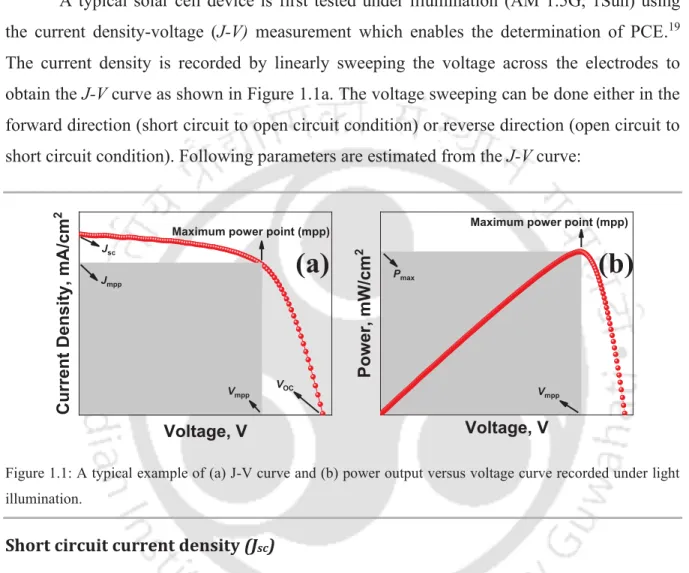
1.3.1•J-V•Characterization•
A typical solar cell device is first tested under illumination (AM 1.5G, 1Sun) using the current density-voltage (J-V)!measurement which enables the determination of PCE.19 The current density is recorded by linearly sweeping the voltage across the electrodes to obtain the J-V curve as shown in Figure 1.1a. The voltage sweeping can be done either in the forward direction (short circuit to open circuit condition) or reverse direction (open circuit to short circuit condition). Following parameters are estimated from the J-V curve:
Figure 1.1: A typical example of (a) J-V curve and (b) power output versus voltage curve recorded under light illumination.
Short•circuit•current•density•(Jsc)•
The short circuit current density is obtained from the J-V curve at zero volt condition.
It is the current per unit area that is induced directly due to the photo-generated charges. The Jsc value depends on the absorption properties and bandgap of the active layer, charge transportation and collection in the complete device.20 Jsc is the maximum current that can be generated in a solar cell.
Open•circuit•voltage•(Voc)•
The open circuit voltage is determined as the potential in the device when the current flowing inside it is zero. The zero current condition arises when the photo-generated charges
Pmax
Vmpp
Power, mW/cm2
Voltage, V
Maximum power point (mpp)
VOC Vmpp
Current Density, mA/cm2
Voltage, V
Maximum power point (mpp) Jsc
Jmpp
(a) (b)
TH-2676_166153004
Introduction Chapter!1!
7 equal the injected charges. It mainly depends on the built-in potential and the band positions of active layer.21 It is the maximum voltage that can be obtained in a solar cell.
Fill•factor•(FF)•
Fill factor is a parameter which is used to evaluate the deviation of solar cell sample efficiency from the estimated theoretical maximum power output. High value of FF indicates good quality of solar cells.22 If the maximum power point (mpp) is known then the FF of a solar cell can be calculated using equation 1.1.
= !""#!""
$%#&% (1.1)
Power•conversion•efficiency•(PCE,• )•
The overall power conversion efficiency of a solar cell is defined as the ratio of maximum power (Pmax) extracted from solar cell to the power of incident light (Pin) and can be expressed as equation 1.2:
'()*+,- = .!/0
.12 = 345675FF8'9: (1.2)
The product of photocurrent and voltage at mpp (Jmpp x Vmpp) results in the maximum power (Pmax) as illustrated in Figure 1.1b. The J-V curve of PSCs often depends on the scan direction resulting in hysteresis behavior. Therefore, the scan direction (Voc to Jsc or Jsc to Voc
sweep of voltage) and the scan rate are important for obtaining reliable photovoltaic parameters.23
1.3.2•External•Quantum•Efficiency•(EQE)•
EQE or incident photon to current efficiency (IPCE) is a ratio of number of photons absorbed by the active layer to the number of charges (electrons and holes) getting collected at the electrodes. It is usually measured to confirm the reliability of Jsc obtained from J-V!
characterization. The EQE spectrum (Figure 1.2) is obtained by applying monochromatic light with continuously varying wavelength. The photocurrent at individual wavelength can be estimated; hence the area under the spectrum gives the integrated Jsc value. EQE of a solar cell device can be estimated using equation 1.3.
TH-2676_166153004
Chapter!1!!!!!!!!!!!!!!!!!!!!!!!!!!!!!!!!!!!!!!!!!!!!!!!!!!!!!!!!!!!!!!!!!!!!!!!!!!!!!!!!!!!!!!!!!!!!!!!!!!!!!!!!!!!!!!Introduction!!
8
);)+<- = :>?>%@A&2$+B-
:"C&@&2$+B- = $%+B- DE
.12EGH =GI
Dl´ $%+B-
.12 * =JKLMl ´ $%+B-
.12 (1.3)
where, nelectrons & nphotons are number of electrons & photons, respectively. Jsc is photocurrent density in mA cm-2, q stands for an elementary charge, Pin is the power of incident light (mW cm-2), h is the Planck’s constant, f is the frequency of light in vacuum (Hz), • is the speed of light in vacuum (nm s-1) and ! is the wavelength of incident light (nm). The expected short- circuit photocurrent density that is to be generated by the solar cell is calculated by integrating the product of IPCE and Jsc (!) over the wavelength of the incoming light.24, 25
Figure 1.2: A typical EQE spectrum of a perovskite solar cell.
1.3.3•Impedance•Spectroscopy•Measurements•
Impedance spectroscopy is a useful technique to track charge transport and recombination involved in a solar cell. The impedance spectroscopic measurement of a solar cell is performed, generally, in the frequency range of 1 Hz–1 MHz with sinusoidal voltage amplitude of 10 mV in dark condition. The impedance data can be represented in the form of either Bode plot or Nyquist plot. By fitting the impedance spectrum to equivalent circuits, many parameters such as sheet resistance, shunt resistance, charge transport resistance, recombination resistance, capacitance, and density of trap states can be estimated.26-28
1.4•Generations•of•Solar•Cell•
Photovoltaic technologies have come through decades of evolution and are well classified into four generations (Figure 1.3). In the first generation, solar cells were mainly
TH-2676_166153004
Introduction Chapter!1
9 based on crystalline silicon wafers which are hundreds of micrometer thick. These solar cells are fabricated using the diffusion process of the crystalline silicon wafers. The highest PCE using the crystalline silicon have reached 27.6% in single junction and 47.1% in four- junction devices. Currently, silicon wafer based solar cells are commercially dominant and account for majority of the terrestrial solar cell industry. The reason for such a strong hold is its long payback lifetime of 25-30 years. Although this solar cell technology is commercially most viable still the production of solar grade silicon wafer is very costly, tedious and large energy consumption process. Also, the thick wafers resulted in heavier solar modules which restricted its use in space applications. Further, they generate waste in the range of thousands of metric tons which is increasing every year.29-31
Figure 1.3: Classification of four generations of solar cell.
The drawbacks of the silicon wafer usage in solar cells directed the way to the discovery of thin film based solar cells in the second generation. In this generation amorphous silicon, CdTe and CIGS are utilized in solar cells fabrication. The cost of production for obtaining these materials for developing solar cells is less compared to crystalline silicon and since, thin films are used to generate electricity the photovoltaic cells were much cheaper than the first generation solar cells. The second generation solar cells also has comparable payback lifetime as the crystalline solar cells, but the PCE has only reached 14.0%, 22.1% and 23.4% for amorphous silicon, CdTe and CIGS, respectively.
Since, thin films were being used in the development of the solar cells; the modules are light weight and finds majority of the application in space application. This materials used in the second generation are scarce elements and obtaining pure form of the materials involves
Generations!of!Solar!Cell
First!Generation (Wafer!based)
Crystalline!Si!- 27.6%
GaAs!- 30.5%!
Second!Generation!
(Thin!Film!based)
Amorphous!Si!- 14.0%
CdTe!- 22.1%
CIGS!- 23.4%-
Third!Generation!
(Organic!Molecule! based)
Organic!- 18.2%
DSSC!–13.0%!
Fourth!Generation!
(Hybrid)
Perovskite!- 25.5%
Quantum!Dot!- 18.1%
Kesterite!- 12.6%
TH-2676_166153004
Chapter!1!!!!!!!!!!!!!!!!!!!!!!!!!!!!!!!!!!!!!!!!!!!!!!!!!!!!!!!!!!!!!!!!!!!!!!!!!!!!!!!!!!!!!!!!!!!!!!!!!!!!!!!!!!!!!!Introduction!!
10
costly process as well as consumes lot of energy. Further, the waste generated from the solar modules is polluting not only earth, but also creating tons of garbage in space.32-35
Thereafter, the focus shifted towards having eco-friendly and inexpensive active materials in the third generation solar cells. In third generation, organic materials such as small materials and polymers are being used in the active layer of the solar cells. Polymers were considered as insulators until, in 1976, Alan J. Heegar, Alan. G. MacDiarmid and Hideki Shirakawa displayed that polyacetylene when halogenated improves conductivity by several orders.36 They received the Nobel Prize in Chemistry for this excellent discovery in the year 2000.37 Many conducting organic molecules were developed and they displayed similar optical and electrical properties as that of inorganic materials that were being used for solar cells in the first two generations. This led to many organic materials being utilized as active layer for polymer/organic solar cells (OSC) and Dye-sensitized solar cells (DSSC).38,
39 These solar cell technology do not form the conventional p-n junction in the device and offers an advantage of being processed using the solution-processable technique and the cost of production is very low. They can also be fabricated on flexible substrates and hence, large- area roll-to-roll solar modules can be developed. Further, these solar cells can be easily disposed and the substrates can be recycled for future use. Since, the cost of material development and device fabrication is very less the payback lifetime for the third generation solar cells are estimated to be much shorter than the previous two generations. However, the growth of these solar cells is limited by its PCE and stability. The highest PCE of 18.2% and 13.0% has been achieved for OSC and DSSC, respectively. On the other hand development of third generation solar cells with stability of a few years is still a challenge and draws a lot of interest from various academicians and industries.40, 41
Finally, fourth generations of solar cells witnessed the utility of hybrid materials such as organic inorganic perovskite, quantum dots-organic, nanoparticle-organic (plasmonic) heterojunction and kesterite as active layer.42-45 These low-cost materials also enable fabrication of solar cells on flexible a mechanically robust substrates. Perovskite solar cells (PSCs), in general, displayed characteristics similar to that of inorganic materials that were being employed in the first two generations of solar cells. Even though the stability is an issue, this fast growing technology in the field of solar cells has PCE reaching from 3% to
TH-2676_166153004
Introduction Chapter!1!
11 over 25% within a span of just over a decade. This solar cell is being tried for various commercial applications by improving its stability. Already, few reports suggest that fourth generation solar cells can be useful for space applications with short term target. The fourth generation solar cells also boast of low payback lifetime, and once the stability is significantly improved to few years this photovoltaic technology can evolve as the best alternative to inorganic solar cells.46
This thesis covers the fabrication of OSC from third generation and PSC from the fourth generation of solar cells. Hot-casting technique was used to fabricate OSC and PSC in the second and third chapters, respectively. The room-temperature anti solvent method was used to develop PSC in the fourth and fifth chapters.
1.5•Organic•Solar•Cell•(OSC)•
OSC belongs to the third generation of solar cells and involves organic semiconductors (polymers or small molecules) as the light absorbing photo-active layer.
Generally, the organic molecules associated in the fabrication of OSC can be easily developed at very low cost and the choice of materials is available in plenty. Solution- processing technique is mostly used in the fabrication of OSCs, making the development process even cheaper even for large volumes and area. This solar cell can be fabricated on flexible substrates and hence, is much lighter in weight compared to its silicon counterpart.
Since, the materials used can be easily disposed its large scale commercialization is most likely to reduce the pollution caused by the inorganic solar cells.47, 48 OSCs utilize either a donor material (p-type) or an acceptor material (n-type) or both in various configurations as active layer. A single layer OSC consists of an organic semiconductor sandwiched in between two contacts one with higher work function and the other slightly lower work function to create the built-in potential so that the photo-generated charges can easily diffuse and gets collected at the electrodes. However, the single layer OSC offers a disadvantage of recombination of the photo-generated excitons, which are bounded holes and electrons, as their diffusion length is small and the charges recombine without reaching the electrode. The built-in potential is not enough to draw the charges towards electrodes, hence very low PCE<1% is achieved in single layer OSCs.49, 50 Following this drawback, bilayer OSCs (planar heterojunction OSCs) were fabricated where two layers, one donor and one acceptor,
TH-2676_166153004
Chapter!1!!!!!!!!!!!!!!!!!!!!!!!!!!!!!!!!!!!!!!!!!!!!!!!!!!!!!!!!!!!!!!!!!!!!!!!!!!!!!!!!!!!!!!!!!!!!!!!!!!!!!!!!!!!!!!Introduction!!
12
was sandwiched in between two electrodes. Different electron affinity and ionization energies of the donor and acceptor materials allowed generation of an electrostatic force at the interface. The excitons that are photo-generated near the interface can be easily separated and collected at the electrodes. However, the snag in this system was that the excitons generated away from the interface still recombined and was a loss in the photovoltaic devices. Thus, the thickness of each layer became very important in fabrication of planar heterojunction devices. Initially, the PCE was limited in bilayer OSCs, but with the development of new donor and acceptor materials the PCE has crossed 14%.51-53 The shortcomings of these two junction types lead to the bulk heterojunction (BHJ) OSCs where the donor and acceptor materials are mixed in a fixed ratio in the solution form before utilizing it to coat the active layer.54-56 This technique formed a nanoscale domain of the donor and acceptor materials in the film which allowed the excitons to separate at each interface easily and the loss is minimized. Among all the junction types, BHJ is most popular and PCE >18% has been achieved.
1.5.1•Working•principle•
The working principle of an OSC involves six important processes for converting the photon energy into electricity (Figure 1.4). The steps are: i) absorption of photons and excitations, ii) generation of excitons, iii) diffusion of excitons at the donor-acceptor interface, iv) formation of polaron, v) charge dissociation, and vi) charge transport and collection. Each steps needs to be taken care of to maximize the utility of light energy and minimize the losses to ensure high PCE of the photovoltaic device. On illumination, OSC absorbs photons from light and the active layer is excited. Thereafter, unlike inorganic solar cells, excitons are formed in the active layer which displays a binding energy of 0.1-1 eV.
These bounded hole-electron pairs in the form of excitons diffuses to the interface of the donor-acceptor materials where the holes and electrons are separated. If the excitons do not diffuse to the interface the photo-generated excitons are lost through non-radiative recombination. Once the excitons reach the interface, electrons moves towards the acceptor material and donor stays in the donor forming the polaron. The charges in polarons can now be easily dissociated and the holes moves deeper in the donor material, whereas the electrons
TH-2676_166153004
Introduction Chapter!1
13 moves deeper in the acceptor. Finally, the holes and electrons are collected at the anode and cathode, respectively.57, 58
Figure 1.4: Working principle of organic solar cell.
Figure 1.5: OSC device architecture (a) conventional, and (b) inverted.
1.5.2•Device•architecture
All the OSC fabricated follows two kinds of device architecture: (i) conventional, and (ii) inverted as presented in Figure 1.5. The inverted device architecture was discovered first where transparent conducting oxide (TCO) is used as anode and a metal counter electrode as cathode. The photo-generated holes gets transported towards and collected at TCO, where the
TCO Counter Electrode
D o n o r
HTL
A c c e p to r
+ +
- -
+
(a) (b)
TH-2676_166153004
Chapter!1!!!!!!!!!!!!!!!!!!!!!!!!!!!!!!!!!!!!!!!!!!!!!!!!!!!!!!!!!!!!!!!!!!!!!!!!!!!!!!!!!!!!!!!!!!!!!!!!!!!!!!!!!!!!!!Introduction!!
14
electrons moves towards and gets collected at metal. However, later the flow of charges was reversed based on the selection of materials for appropriate band alignment so that the electrons gets collected at the TCO and holes at the counter metal. Thus, TCO acted as cathode and metal electrode was anode. Since, the direction of the charges were reversed, hence the name inverted device architecture. Similar charge transport mechanism is followed in both the device architectures.59
Figure 1.6: Most commonly used donor acceptor materials for OSC.
In both the device architectures various components are used namely: (i) anode, (ii) hole transport layer (HTL), (iii) active layer, (iv) electron transport layer (ETL), (v) buffer layer, and (vi) cathode. The conventional devices uses indium doped tin oxide (ITO) as anode, but some low work function metals such as copper or gold as used as anode in inverted devices. PEDOT:PSS is the most common HTL used in OSC for conventional devices. However, for conventional devices MoO3 is the most utilized HTL.60 The active layer for both the device architecture consists of donor and acceptor materials either
/
TH-2676_166153004
Introduction Chapter!1!
15 separately for bilayer devices or blended together in some ratios for BHJ devices. The most common donor materials for OSCs are P3HT, PTB7, PTB7-Th, PBDB-T, etc. The fullerene based acceptors like PC61BM and PC71BM are mostly used. However, recently some non- fullerene acceptors such as ITIC, IDIC, etc. have gained popularity.39 A separate ETL is generally not used in conventional OSCs, but for inverted devices transparent metal oxides such as zinc oxide, tin oxide, titanium oxide, etc. are used.61 Buffer layers are used in OSCs to further increase the transport and collection of the photo-generated charges either through band alignment or through quantum mechanical tunneling. Organic buffer layers commonly used in OSCs are bathocuproine (BCP), Bathophenanthroline (BPhen), etc. and metal buffer layers include calcium, magnesium, etc.62 Finally, for cathode metal counter electrodes such as aluminium and silver are used for conventional devices, but for inverted devices TCOs are only used as cathode. Most commonly used active layer materials used as donor and acceptor in OSC are presented in Figure 1.6.
1.5.3•Engineering•Organic•Solar•Cells•
With the discovery of conducting polymers in 1977, the field of OSC has displayed the ability to bring down the cost of photovoltaic and also reduce the waste generation due to the inorganic solar panels. OSCs can be fabricated on low-cost solution-processable technique and can be easily integrated on flexible substrates. Short payback lifetime is another major advantage of OSC. Thorough materials and device engineering have resulted in PCE reaching beyond 18%. The most common technique to achieve good performance in an OSC device is to vary the ratio of donor and acceptor material in the blend solution for depositing the BHJ active layer. Modulating the ratio of donor and acceptor materials result in optimum domain size in nanoscale for smooth diffusion and transport of the photo- generated charges.63, 64 Fabrication of ternary OSC through introduction of a third component (either a donor or an acceptor) bearing complementary absorption also tunes the morphology of the active layer and improves the device performance.65, 66 The active layer is further annealed, if required, for the removal of excess solvent from the film. Solvent vapor annealing is another approach that has improved the morphology of the active layer further and improved the solar cell PCE.67 It has been also observed that annealing, at times, leads to degrading the active layer and hence, the device performance drops. In those cases, the
TH-2676_166153004
Chapter!1!!!!!!!!!!!!!!!!!!!!!!!!!!!!!!!!!!!!!!!!!!!!!!!!!!!!!!!!!!!!!!!!!!!!!!!!!!!!!!!!!!!!!!!!!!!!!!!!!!!!!!!!!!!!!!Introduction!!
16
annealing technique is replaced by high vacuum treatment of the active layer for removal of excess solvent from the film.68 The transport materials have been also modified to find the adequate band alignment for the smooth collection of charges at the electrodes.69 The processing of blend solution using various green solvents has also reduced the pollution and health issues due to the halogenated solvents. The desirable nanoscale morphology of the active layer processed using green solvents has been also achieved and the performance of the solar cell device has not been compromised.70 Introduction of additives have also acted as morphology modifier and a small percentage have also improved and stabilized the solar cell performance.71
As mentioned before, that since annealing sometimes restricts the charge transport process by hampering the morphology, hence various other methodology have been attempted to improve the device performance especially in PTB7 and PTB7-Th based OSCs.
One very effective technique is cooling a hot ink method where the blend solution is heated for adequate mixing of the donor and acceptor and cooling it down to a lower temperature before coating at room temperature.72 The PCE of the device improved compared to the one which was processed through annealing. Another approach is hot-casting technique using which the blend is coated on a pre-heated substrate and do not require further annealing for evaporation of the excess solvent to achieve PCE >9%. Modulation of thickness and morphology took place by varying the hot-casting temperature. It has also been observed that annealing the active layer after hot-casting may also improve the device performance slightly.73, 74
Large-area and thick active layer OSCs have also been displayed by various device engineering. Techniques such as doctor blading, ink-jet printing and spray coating are very effective in fabricating large-area, flexible OSCs. The possibility of developing an OSC on a fabric has also been displayed.75-77
1.6•Perovskite•Solar•Cell•(PSC)•
PSCs belong to the fourth generation of solar cells and include materials in the active layer bearing similar crystal structure to that of CaTiO3. The material is named after the famous Russian mineralogist L. A. Perovski.78 The light harvesting material used for solar
TH-2676_166153004
Introduction Chapter!1
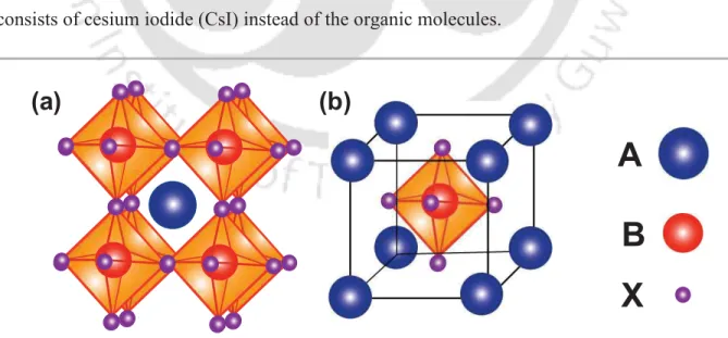
17 cell application is mostly hybrid organic-inorganic lead or tin halide-based material.
Recently, all inorganic perovskite materials are also being utilized in fabrication of solar cells. Similar to CaTiO3, the photo-active material for PSC follows the ABX3 crystal structure where A and B are cations and X is an anion (Figure 1.7). In a perovskite crystal, B and X will form a regular octahedron, BX6, with B in the centre and A is present in the cube- octahedral void. The material offers the many advantage such as ambipolarity, wide range absorption, long diffusion length, long carrier lifetime, tunable bandgap. Alike OSCs, PSCs are also fabricated mostly using solution processing technique which makes this solar cell technology inexpensive.44, 79, 80 The most common perovskite material used for solar cell developments is methyl ammonium lead halide (MAPbX3). This was first used as sensitizer in DSSC in 2009 and resulted in a PCE of 3.8%.18Various developments over the last decade has resulted in PCE reaching beyond 25% and is well competing with single junction silicon solar cell.81 Even PSCs on flexible substrates have demonstrated high efficiency >20%
making this photovoltaic technology lighter in weight compared to the inorganic counterpart.82 Generally, the active layer of a solution-processable PSC is developed from a precursor solution consisting of organic [methyl ammonium iodide (MAI), formamidinium iodide (FAI), etc.] and inorganic [lead iodide (PbI2), tin iodide (SnI2), etc.] materials in fixed ratio. These materials are made soluble in solvents such as dimethylformamide (DMF), •- Butyrolactone (GBL), dimethyl sulfoxide DMSO, etc. All inorganic perovskite solar cells consists of cesium iodide (CsI) instead of the organic molecules.
Figure 1.7 Scheme of perovskite crystal unit cell (a) A-cation centered and (b) B-cation centered.
A B X
(a) (b)
TH-2676_166153004
Chapter!1!!!!!!!!!!!!!!!!!!!!!!!!!!!!!!!!!!!!!!!!!!!!!!!!!!!!!!!!!!!!!!!!!!!!!!!!!!!!!!!!!!!!!!!!!!!!!!!!!!!!!!!!!!!!!!Introduction
18
Figure 1.8: Working principle of perovskite solar cell.
1.6.1•Working•Principle
Identical to silicon solar cell, the working principle of a PSC involves three important processes for converting the photon energy into electricity (Figure 1.8). The steps are: i) absorption of photons and excitations, ii) generation of charges, iii) charge transport and collection. On illumination of the solar cells, holes and electrons are generated due to absorption of the photons. The photo-generated holes move to the HTL through the HOMO level, whereas the electrons move towards the ETL through the LUMO level. Finally, these charges are collected at the respective electrodes. There is some debate regarding the formation of excitons instead of free electron-hole pairs. Few reports suggest that the lower dimensional PSCs have excitonic charge transport. Hence, in these cases first the excitons are broken into free charges and then the remaining process follows. 83
Figure 1.9: PSC device architecture (a) mesoscopic, (b) planar conventional and (c) planar inverted.
TCO Counter Electrode
Perovskite
HTL ETL
+ -
+
- -
(a) (b) (c)
TH-2676_166153004
Introduction Chapter!1!
19 1.6.2•Device•Architecture•
The device architecture of PSCs is broadly classified into two types: (i) mesoscopic structure and (ii) planar heterostructure structure as presented in Figure 1.9. The mesoscopic structure facilitates infiltration of perovskite into a metal oxide layer which is mesoporous in nature. However, the ambipolarity of the perovskite material is not explored completely in this architecture. Hence, the planar heterojunction PSCs were fabricated to probe the ambipolar nature of perovskite. The planar devices are sub-classified into two types: (i) conventional (n-i-p) and (ii) inverted (p-i-n). If an n-type contact is present towards the TCO then it is said to be conventional planar device, while a p-type contact with TCO defines an inverted planar device. All the device architectures follow similar charge generation, transport and collection mechanism as explained in the working principle of PSCs.84, 85
The components of PSCs of varied architecture are classified similar to OSCs as: (i) anode, (ii) hole transport layer (HTL), (iii) active layer, (iv) electron transport layer (ETL), (v) buffer layer, and (vi) cathode. The mesoscopic and conventional devices use some low work function metals such as copper or gold as used as anode, while the inverted devices uses TCO such as fluorine doped tin oxide (FTO) or ITO as anode. Spiro-OMeTAD is the most common HTL used in mesoscopic and conventional devices. Since spiro-OMeTAD is expensive, many conjugated organic materials are also used as HTL in mesoscopic and conventional devices. For the inverted device, PEDOT:PSS and few conjugated polyelectrolytes are the most common HTLs that are being utilized. However, recently inorganic HTL such as NiOx has been also explored for PSCs with improved device performance.86, 87 The most commonly used single cation perovskite for active layer in PSCs is MAPbX3 or FAPbX3 or CsPbX3. However, double and triple cation perovskites (consisting of MA+, FA+ and Cs+ in varying ratios) have also garnered interest.88 Mesoporous titanium oxide is the most common ETL used in mesoscopic architecture. In the conventional devices titanium oxide or tin oxide are commonly used as ETL, while the inverted devices utilizes PC61BM or fullerene (C60) as ETL.89-91 Like the OSCs, buffer layers are also used in PSCs to further increase the transport and collection of the photo-generated charges either through band alignment or through quantum mechanical tunneling. Buffer layers commonly used in PSCs are BCP, Rhodamine-101, etc.88 Finally, for cathode TCOs are only used in
TH-2676_166153004
Chapter!1!!!!!!!!!!!!!!!!!!!!!!!!!!!!!!!!!!!!!!!!!!!!!!!!!!!!!!!!!!!!!!!!!!!!!!!!!!!!!!!!!!!!!!!!!!!!!!!!!!!!!!!!!!!!!!Introduction!!
20
mesoscopic and conventional devices, while for inverted devices metal counter electrodes such as aluminium and silver are used as cathode.
1.6.3•Engineering•Perovskite•Solar•Cell•
PSCs have fascinated tremendous research interest in the field of photovoltaic technology. As already discussed before, this is due to the attractive optoelectronic properties that perovskite materials have facilitated in demonstrating PCE beyond 25% in solar cell devices. Still, the devices fabricated from the perovskite materials show stability only in the range of few hours to few days and are yet to compete with the inorganic solar cells based on the lifetime. The trap states present in the perovskite tends to accelerate the degradation process when exposed to heat, light, oxygen or UV radiation.92-96 With PCE almost nearing the Shockley-Queisser limit, the complete focus has now mostly shifted to fabricating solar cells with improved stability under ambient conditions.97-100 The first and foremost prerequisite to have some stability in PSCs is to fabricate perovskite films with improved crystallinity. The traps present in the perovskite crystals tend to reduce the stability. Also, the perovskite film quality is observed to increase the performance of the device.101-103 Many techniques such as anti-solvent method, hot-casting, vacuum treatment, compositional engineering, etc. have been developed to improve the quality of perovskite films and increase its crystallinity.104-107 Obtaining large sized crystalline grains with minimum width of grain boundaries is also a pre-requisite to further augment the stability and performance of the devices. Perovskite films with millimeter-sized grains and nanometer-sized grain boundary width have been developed to ambient stability of the device.108 Another effective strategy to reduce the trap density of perovskite is introduction of organic molecules as passivating additive (Figure 1.10) in the precursor solution.109-113 These molecules interact with each components of the precursor solution and control the crystallization process from the initial stages. The functional groups present in the organic molecules passivate the defects present in the perovskite layer and mitigate ion migration arising due to the presence of defects. It has also been observed that the organic molecules are coated on top of the perovskite films for adequate surface passivation. Both these techniques also result in reduced hysteresis in the forward and reverse scans of the current-voltage characteristic curve.
TH-2676_166153004
Introduction Chapter!1!
21 Another strategy to increase the stability of PSCs is to reduce the dimensionality of the perovskite crystal. The two-dimensional (2D) Ruddlesden-Popper and Dion-Jacobson perovskites have engrossed researchers to fabricate solar cell devices with even longer stability. The 2D perovskites are formed by combining large organic cations such as phenyl- ethyl ammonium (PEA), and butyl ammonium (BA) with the other components in the precursor solution. However, the PCE have only reached ~20% using these 2D perovskites due to quantum confinement effect.114-117 Thereafter, formation of 2D/3D interface in the perovskite film has been attempted. This device engineering confirms the efficient charge transport property of the 3D perovskite and enhanced stability of the 2D perovskite. This technique has facilitated PSCs to display more than one year stability without losing much on PCE.118 Another problem with PSCs is the lead (Pb) content as even a small amount of Pb exposure may result in severe health issues in human being including death. Thus, focus has now shifted to fabrication of Pb-free or Pb-less PSCs. The Pb-free (tin-based) PSCs have resulted in PCE ~10% and Pb-less (or less-Pb) PSCs have reached ~19% PCE.119-123
Figure 1.10: Commonly used organic passivating molecules used in PSC.
/
TH-2676_166153004