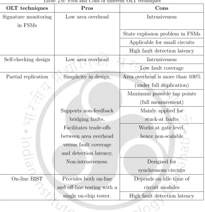
Most of the OLT schemes are designed for synchronous circuits as compared to asynchronous circuits. The area overhead of these schemes is very high due to Mutex blocks which are the main components of the online tester.
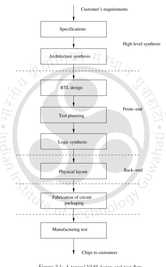
Introduction
- Introduction to OLT of digital VLSI circuits
- Introduction to decision diagrams and their appli- cations in digital circuit testingcations in digital circuit testing
- Motivations and Contributions of the thesis
- Organization of the thesis
Finally, the motivations and contributions of the dissertation in the field of OLT digital VLSI circuitry are discussed in Section 1.3. In most of the works on OLT digital circuits, the individual fault model s-a is considered.
Literature review: On-line Testing of Digital VLSI Circuits and Decision
Digital VLSI testing
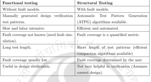
- Structural vs. functional testing
- Fault models
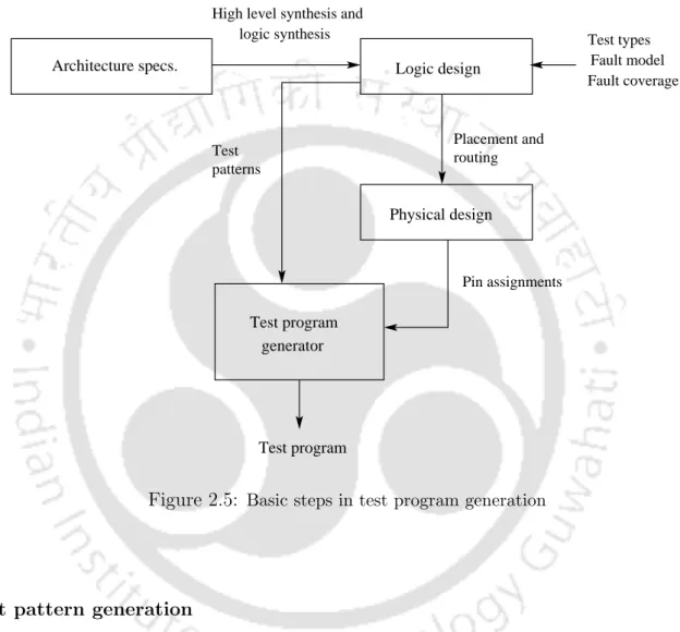
- Test programming
- Comparison of ATE based testing, BIST and OLT
In a modified 32-bit adder, the carry input to the ith (full) adder is multiplexed with the ith bit of the input shift register, 1≤i≤31. At the circuit level, the inputs must be preceded by a multiplexer to connect to the normal (functional) inputs or outputs of the test pattern generator.
Literature review: On-line testing of digital VLSI circuitscircuits
- Signature monitoring in FSMs
- Self-checking design using error detecting codes
- Duplication schemes for OLT
- On-line BIST
- Pros and cons of different OLT techniques
Most of the partial replication-based OLT schemes reported in the literature seem to work for single s-a faults. Another assumption is regarding the touching of the CUT lines by the online tester.
![Table 2.3: Merits and demerits of ATE based off-line structural testing [2, 17]](https://thumb-ap.123doks.com/thumbv2/azpdfnet/10442093.0/51.892.145.813.173.763/table-merits-demerits-ate-based-line-structural-testing.webp)
Desired features of OLT schemes
- Measurement limitation based flexibility in OLT
- OLT schemes for advanced fault model
- OLT schemes for circuits at higher description level
- OLT schemes for asynchronous circuits
The OLT schemes reported in provide flexibility in terms of trade-offs between area overhead versus fault coverage and detection latency by selecting a subset of the test patterns. Now we discuss some high-level fault models based on behavioral or functional description of the circuit.
Complexity of generation of exhaustive set of test patterns for OLTpatterns for OLT
- Decision Diagrams
- Testing of digital circuits using Decision Diagrams
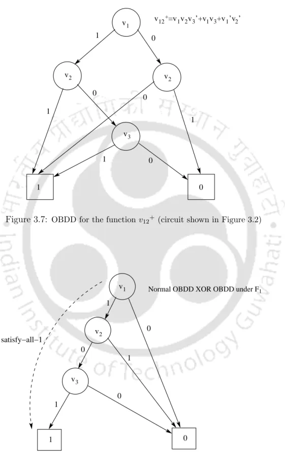
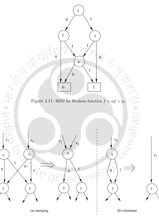
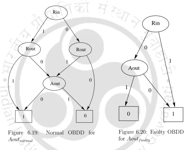
Each non-terminal node of a BDD is associated with one input variable of the Boolean function. Each output of the circuit is represented using separate OBDDs under normal and fault conditions (say OBDDnormal and OBDDf fault). Scalability: In the case of OLT scheme at higher description level such as behavioral level, register transfer level, etc., the procedure of generating test patterns using OBDDs cannot be applied because OBDDs model the circuits at the gate level.
Conclusion
Overfeedback error: The simple XOR-based procedure of generating test patterns using OBDD may not be a straightforward approach to overfeedback errors because in some cases they create oscillations. OLTs for asynchronous circuits: OBDDs have not yet been applied to OLTs of asynchronous circuits. So, a study is required to find out whether the XOR-OBDD procedure is applicable to OLT of asynchronous circuits.
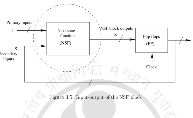
On-line Testing with Measurement Limitation
Introduction
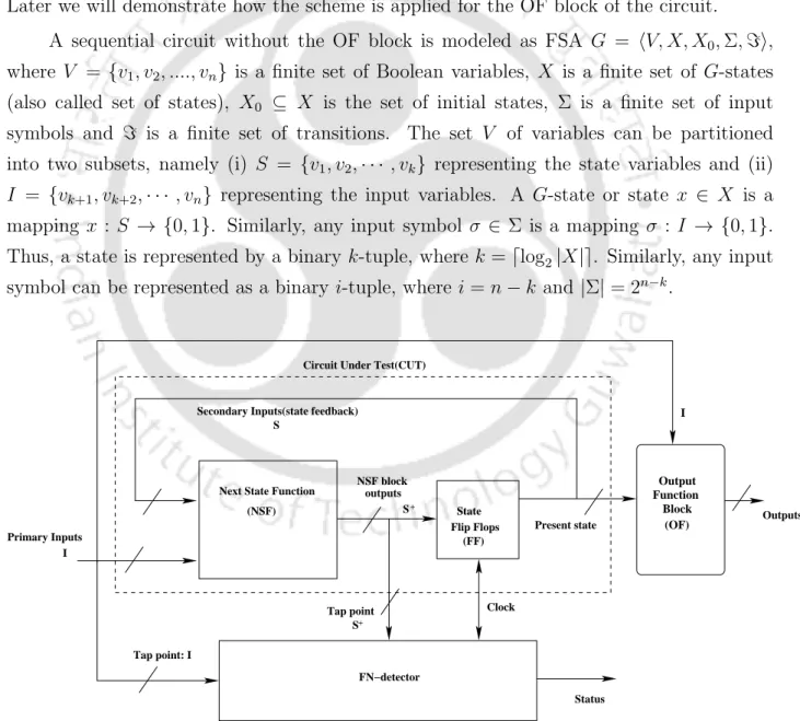
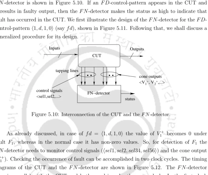
It can be noted that measurement limitation reduces load (fan outlet) on the gates of the SUT driving the tap points. Experimental results on ISCAS 89 benchmarks were presented, illustrating that measurement constraint can be used as a trade-off parameter to minimize area overhead to a large extent with minimal compromise in error coverage and detection latency. In Section 3.2, we discuss circuit modeling using Finite State Automata (FSA) framework and FN detector construction under measurement constraint.
FSA framework under measurement limitation
Circuit modeling and F N -detector design
Circuit modeling under single stuck-at fault
The FSA circuit model (covering the normal and fault states) can be conveniently thought of as a collection of subsystems, one for the normal state and one for the faults F1, F2,· · · , Fp. When we need to distinguish between normal and faulty subsystems, the states for normal subsystems are denoted as x0j, 1≤j, and the states of Fi-submachines as xij, 1≤j; same for transitions. Equivalent states of measurements: Two states x1 and x2 are equivalent to a measurement denoted as x1Ex2 if x1|Sm =x2|Sm.
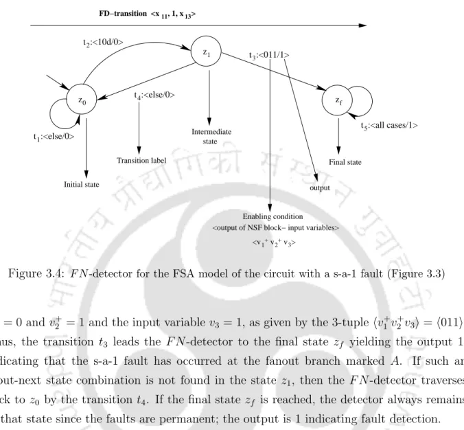
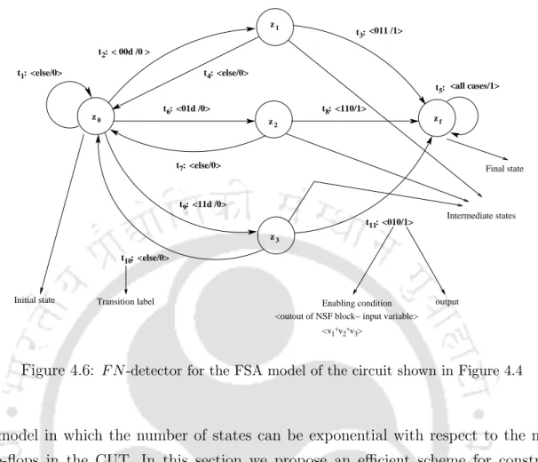
F N -detector design for FSA model of a circuit
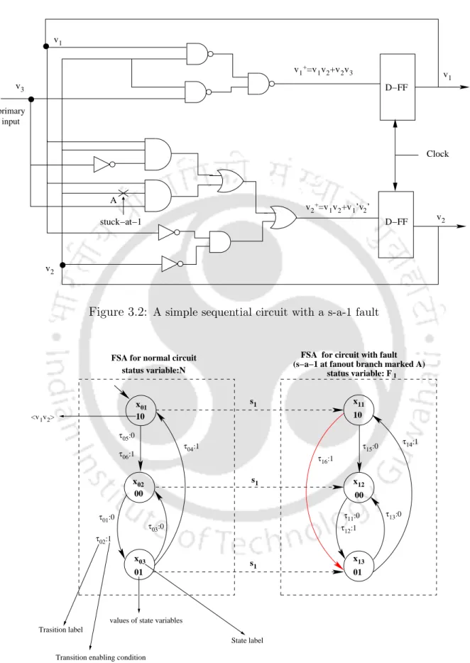
State z1 is reached by transition t2 when CUT goes to state x11 =initial(τ16), i.e. the measured NSF output blocks v1+ and v2+ are 1 and 0, respectively. If then the input v3 is measured as 1 and v+2 is measured as 1, the final state F of the N-detector is visited, indicating a fault in F1. After that, if v1+v2+ is measured as 01, the final state F of the N-detector is visited, indicating a fault in F1.
Efficient construction of F N -detector
- OBDD based procedure for exhaustive test pattern genera- tion for the NSF block under full measurementtion for the NSF block under full measurement
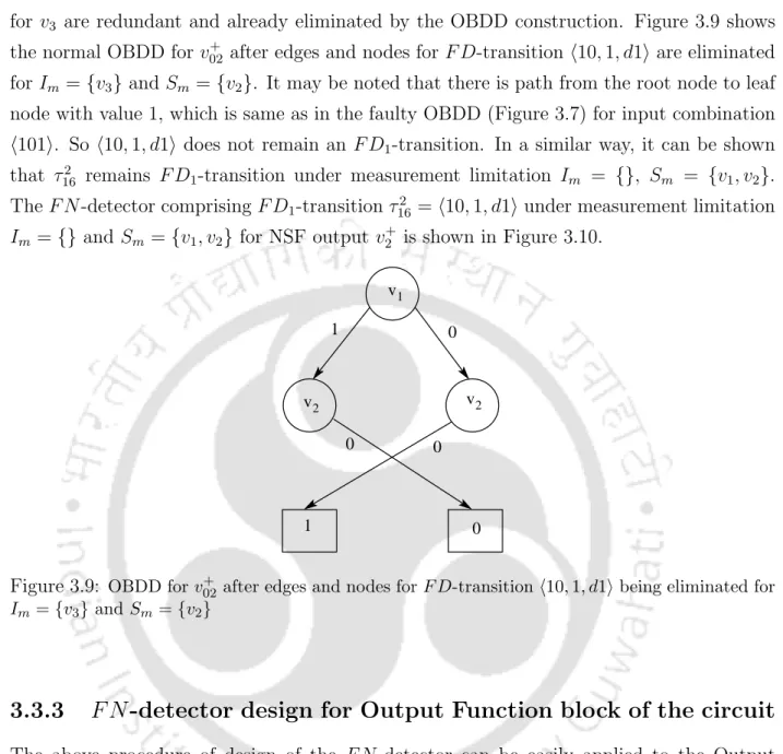
- OBDD based procedure for determination of F D-transitions under measurement limitationunder measurement limitation
- F N -detector design for Output Function block of the circuit
In this section we discuss the procedure for exhaustive test pattern generation for a faultFi for a given output line of the NSF block (under full measurement). Since the OF block is a combinational circuit, its F N detector design is much simpler than that of the NSF block. It can be noted that the error detection in the OF block is performed in a single clock cycle, whereas it requires two consecutive clock cycles for the NSF block in the circuit.
Experimental evaluation
- Trade-offs in F N -detector design: detection latency, fault coverage, measurement limitation and area overheadcoverage, measurement limitation and area overhead
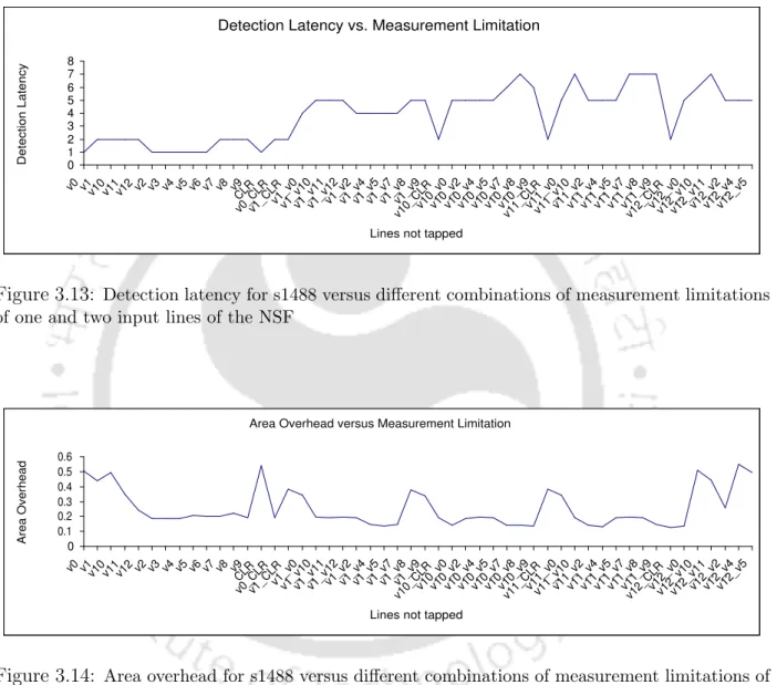
First, we illustrate the results (as graphs) for fault coverage, detection latency, and area overhead of the circuit s1488 under different combinations of measurement constraints. Area Overhead (AO): Area Overhead=(Area of the FN detector after synthesis)/(Area of the CUT after synthesis). For a given detection latency region, the overhead for the proposed scheme is lower compared to that of [12, 36].
Conclusion
This range can be used as a design parameter to balance area overhead against detection latency. The scheme of [12, 36] randomly eliminates FD transitions, while the proposed scheme performs this elimination by not measuring some input lines. Failure to measure some input lines of the NSF implies that they are not being monitored by the FN detector.
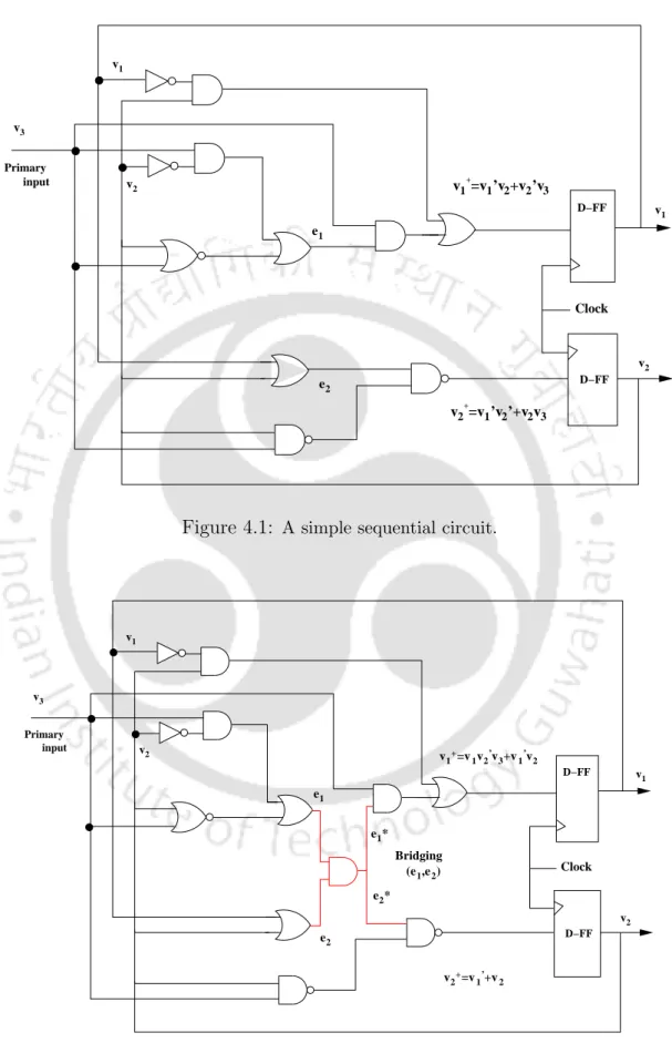
On-line Testing for Feedback Bridging Faults
Introduction
The scheme first defines bridge faults that do not lead to oscillation, i.e. all non-feedback faults and some feedback coupling faults. Experimental results illustrate that considering feedback coupling faults along with non-feedback faults improves fault coverage with a marginal increase in overhead compared to schemes that only include non-feedback faults. The Finite State Automata (FSA) based modeling of the circuit under test (CUT) with connection faults and the construction of the F N detector is explained in Section 4.2.
Circuit modeling and FN-detector design using FSA frameworkFSA framework
- Circuit modeling under bridging faults
- F N -detector construction from the FSA model of the CUT
In most of the works on bridging faults, short is assumed between any two lines in the SUT. Fault is modeled as part of the same FSA used to model the SUT under normal condition. A bridging fault in the flip-flops can be represented by using a bridging fault involving the input and output lines of the NSF block.
Efficient construction of F N -detector for bridging faultsfaults
- Partition of the CUT into sub-circuits using cones of influenceinfluence
- OBDD based procedure for generation of exhaustive set of F D-transitions for non-feedback bridging faultsF D-transitions for non-feedback bridging faults
- OBDD based procedure for generation of exhaustive set of F D-transitions for feedback bridging faultsF D-transitions for feedback bridging faults
- OBDD based procedure for illustration of an oscillating feedback bridging fault
The separation of the NSF block (under normal conditions) using impact cones at the NSF outputs is shown in Figure 4.7. The division of the NSF into cones at its exits and the dominant line are also shown in the figure. The division of the NFS into cones at its exits and the dominant line are also shown in the figure.
Experimental evaluation
- Fault coverage analysis
- Area overhead analysis
So if all feedback bridging faults expire, there is a significant drop in fault coverage. Area Overhead (AO): = Area of the F N detector (after synthesis) Area of the circuit under test (CU T). It can be noted that the scheme reported in [13] only handles non-feedback bypass errors.
Conclusion
On-line Testing at Register Transfer Level
Introduction
However, unlike using OBDD for gate-level circuits (in Chapters 3 and Chapter 4), this scheme uses High Level Decision Diagram (HLDD) for circuits at RTL. Finally, an online tester called Fault versus Normal condition detector (F N detector) is designed using these FD check patterns. The generation of the comprehensive set of FD control patterns and the design of the FN detector are discussed in Section 5.4.
High-Level Decision Diagram
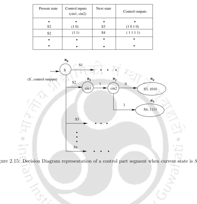
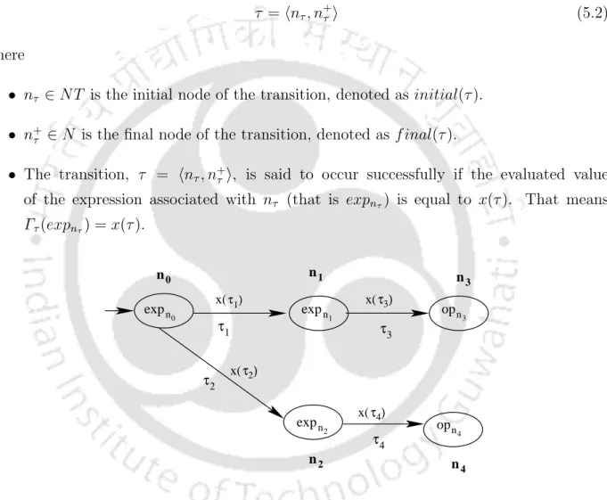
The transition, τ = hnτ, n+τi, is said to be successful if the evaluated value of the expression associated with nτ (that is, expnτ) is equal to x(τ). The value obtained from λi(opni) is referred to as the output of the path, from the initial node to the terminal nodes in the model. For example, the value obtained from λ4(opn4) is referred to as the output of the path from n0 to n4.
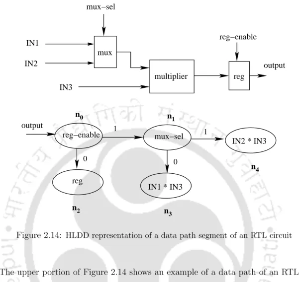
Circuit modeling at RTL: Normal and faulty con- ditionsditions
- Circuit modeling using HLDD
- RTL fault model and circuit modeling under fault
The data path does not perform operations for all possible values of the control signals. Testing a circuit in RTL requires testing the data path and the control part of the circuit. In the next subsection we illustrate one of the RTL fault models presented in [59] and in the following, the modeling of a faulted circuit [59] using HLDD is discussed.
Generation of exhaustive set of F D-control-patterns and design of F N -detectorand design ofF N-detector
- Design of F N -detector
- F N -detector design for combinational part of the RTL circuitcircuit
The division of the SUT using cones of influence in relation to the registers is shown in Figure 5.3. The state transition diagram of the F N detector of the SUT to detect F1 is shown in Figure 5.11. The procedure for designing the F N detector for the combinational part of the RTL circuit is similar to that of the sequential part of the circuit.
Experimental evaluation
- Fault coverage analysis
- Area overhead analysis
The error coverage of the proposed scheme and the existing schemes ([36] and [12]) are almost the same, but the time taken to generate the F D control patterns is much lower than the time taken to generate the test patterns generate in [36 ] and [12]. Increasing the detection latency results in reducing the area overhead of the FN detector. For a given detection latency, the area overhead of the proposed scheme is always less compared to [36] and [12].
Conclusion
In RTL, we can determine the invalid FD control patterns for a fault and drop them into the FN detector circuit design, which can further reduce the overhead space. While in case of gate level circuits there is no such function to decide invalid test patterns for a fault. So in the gate-level case, we include all the test patterns for a flaw in the online tester design, which increases the overhead.
On-line Testing of Speed Independent Asynchronous Circuits
Introduction
In the case of OLT for synchronous circuits, the online test circuit is a Finite State Machine (FSM) which detects the occurrence of F D transitions (the procedure is discussed in Chapter 3 and Chapter 4). A synchronous circuit can be synthesized in a straightforward manner from the FSM specification that performs online testing. In Section 6.2, we discuss the modeling of an SI circuit using the STG under normal and faulted conditions.
SI circuit modeling using Signal Transition Graph and generation of F D-transitionsand generation ofF D-transitions
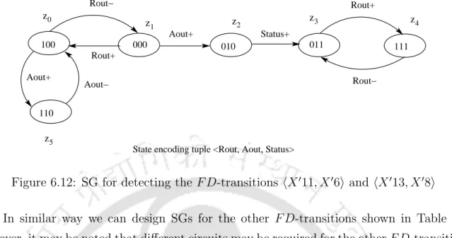
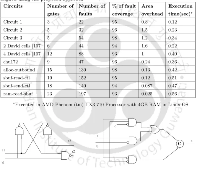
Finally, we discuss the procedure for generating F D transitions in an efficient way directly from the circuit description using the Ordered Binary Decision Diagram (OBDD), without explicitly constructing the SG models, whose complexity can be prohibitively high for large circuits. PN models a system using interface behavior, which is represented by allowed sequences of transitions or traces. The SI circuit shown in Figure 6.1 (taken from [71]) will be considered Circuit Under Test (CUT) to illustrate our proposed scheme.
C2Rin
Converting STG into State Graph model and generation of F D-transitionsF D-transitions
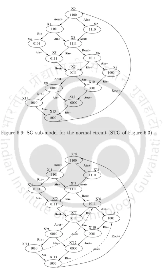
A transition hx, x+i, wherex(C)6=x+(C), is called ansi-transition (start of errorFi), indicating the first appearance of errorFi in the circuit. The SG submodel for the circuit undern1 stuck fault in C2 is shown in Figure 6.10. The SG submodel for the circuit under p1 stuck fault inC1 is shown in Figure 6.11.
Design of F N -detector using F D-transitions
- Circuit synthesis for F N -detector
For example, if Rin, Rout, Ain and Aout are measured to be 1,0,1 and 0 in the initial state of the detector, the detector moves to the intermediate state corresponding to FD transition hX011, X06i. The third bit represents the status output of the detector, which is 0 until the FD transition is detected. Furthermore, the signal is different in the initial state of the corresponding normal transition that also produces the same change.
Efficient generation of F D-transitions directly from circuit description using OBDDcircuit description using OBDD
This operation on the XORed OBDD produces a set of following states reached by the CUT upon triggering the vk signal (rising or falling) below the defective Fi. If Fi affects the falling signal vk, ie. vk−, then remove the next states from N Svk, where the value of vk is 1. Once the required set of next states is determined (either N Svk+ or N Svk−), then for each state ns ∈ N Svk+ (N Svk−), its corresponding the initial/present state (say ps) is obtained by changing only the value of vk in ns from 1 (0) to 0 (1), leaving the other values of the signal unchanged.
Experimental evaluation
- Mutex approach to testing [107]
- Comparison with the Mutex approach
So, for comparing the upper surface of the proposed scheme with [107], we require only half of the resources used in [107]. In the detector of the proposed scheme, there is no dependency on Mutex elements. The Mutex approach verifies online that the CUT output follows the specified handshaking protocol.
Conclusion
It can be noted that the proposed scheme verifies that there are no s-a errors, while the Mutex approach verifies a protocol. In this work, we could not compare error coverage of our approach with the Mutex approach. It can be noted that the circuits considered in the Mutex-based OLT scheme [107] were simple.
Conclusions and Future scope of work
Summary of the work
Furthermore, it is also found that for a given detection delay, the area overhead of the proposed scheme is lower compared to other similar schemes reported in the literature. Furthermore, it has been shown that the increase in area overhead of the on-line tester due to consideration of feedback bridging faults is marginal compared to the case involving only the non-feedback bridging faults. Several circuits are considered as case studies and the area overhead ratios of the detectors are studied.
Future scope of work
To make the OLT scheme more robust, testing of the online tester is needed. Testing of the online tester can be performed either online or offline. The partial replication-based technique discussed in the thesis can be applied for OLT of the online tester.