저작자표시-비영리-변경금지 2.0 대한민국 이용자는 아래의 조건을 따르는 경우에 한하여 자유롭게
l 이 저작물을 복제, 배포, 전송, 전시, 공연 및 방송할 수 있습니다. 다음과 같은 조건을 따라야 합니다:
l 귀하는, 이 저작물의 재이용이나 배포의 경우, 이 저작물에 적용된 이용허락조건 을 명확하게 나타내어야 합니다.
l 저작권자로부터 별도의 허가를 받으면 이러한 조건들은 적용되지 않습니다.
저작권법에 따른 이용자의 권리는 위의 내용에 의하여 영향을 받지 않습니다. 이것은 이용허락규약(Legal Code)을 이해하기 쉽게 요약한 것입니다.
Disclaimer
저작자표시. 귀하는 원저작자를 표시하여야 합니다.
비영리. 귀하는 이 저작물을 영리 목적으로 이용할 수 없습니다.
변경금지. 귀하는 이 저작물을 개작, 변형 또는 가공할 수 없습니다.
Ph. D. DISSERTATION
Machine Learning Strategy for Predicting Process Variability Effect in Ultra-scaled GAA FET
and 3D NAND Flash Devices
초소형 GAA FET 소자 및 3D NAND Flash 소자의 공정 변동성 영향을 예측하기 위한 기계
학습 전략
BY Kyul Ko August 2020
DEPARTMENT OF ELECTRICAL AND COMPUTER ENGINEERING COLLEGE OF ENGINEERING SEOUL NATIONAL UNIVERSITY
Machine Learning Strategy for Predicting Process Variability Effect in Ultra-scaled GAA
FET and 3D NAND Flash Devices
초소형 GAA FET 소자 및 3D NAND Flash 소자의 공정 변동성 영향을 예측하기 위한 기계
학습 전략
지도 교수 신 형 철
이 논문을 공학박사 학위논문으로 제출함
2020 년 8 월
서울대학교 대학원
전기정보공학부
고 결
고결의 공학박사 학위논문을 인준함
2020 년 8 월
위 원 장 최 우 석 (인)
부위원장 신 형 철 (인)
위 원 김 장 우 (인)
위 원 강 명 곤 (인)
위 원 김 윤 (인)
ABSTRACT
This paper presents a Machine Learning (ML) approach for accurately predicting the effects of various process variation sources on ultra-scaled GAA FET devices and 3D NAND Flash Memories. The effects of process variability sources cause various reliability problems in logic and memory devices. In particular, accurate prediction and control is essential by reducing the margin that determine the yield of logic and memory devices.
The machine learning system is largely divided into three classes: Unsupervised Learning, Supervised Learning, and Reinforcement Learning. Among them, a supervised learning series machine learning system, which uses a regression method to train predictive models based on input and output (Training data) values, is the most suitable method for analyzing device characteristics and predicting variability effects. Since the machine learning system of the supervised learning series needs to predict the characteristics of various devices of various variability sources, it is possible to use multiple input-multiple outputs (MIMO) based on complex algorithms (artificial neural networks) with multiple nodes (MN).
In the early stages of the ML system, the variability sources of a single transistor is analyzed. We propose an accurate and efficient machine learning approach which predicts variations in key electrical parameters using process variations (PV) from ultra-scaled gate-all-around (GAA) vertical FET (VFET) devices. The proposed machine learning approach shows the same accuracy and good efficiency when compared to 3D stochastic Technology-CAD (TCAD) simulation. Artificial Neural Network Based (ANN) machine
learning algorithm can perform Multi-input-Multi-Output prediction very effectively.
As an advanced stage of the ML system, we propose a variability-aware ML approach that predicts variations in the key electrical parameters of 3D NAND Flash memories. For the first time, we have verified the accuracy, efficiency, and generality of the predictive impact factor effects of ANN algorithm-based ML systems. ANN-based ML algorithms can be very effective in MIMO prediction. Therefore, changes in the key electrical characteristics of the device caused by various sources of variability are simultaneously and integrally predicted. This algorithm benchmarks 3D stochastic TCAD simulation, showing a prediction error rate of less than 1% as well as a calculation cost reduction of over 80%. In addition, the generality of the algorithm is confirmed by predicting the operating characteristics of the 3D NAND Flash memory with various structural conditions as the number of layers increases.
Keywords : Process Variation (PV), Machine learning (ML), Artificial neural network (ANN), Gate-all-around (GAA), Vertical device, NAND Flash Memories, Prediction.
Student number :2015-20882
CONTENTS
Abstract ---
iChapter 1. Introduction 1.1. Emergence of Ultra-scaled 3D Device ---1
1.2. Increasing Difficulty of Interpreting Variability Issues ---5
1.3. Need for Accurate Variability Prediction --- 10
Chapter 2. Machine Learning System 2.1. Introduction --- 15
2.2. Analysis of Variability through TCAD Simulation --- 17
2.3. Structure of Machine Learning Algorithm --- 25
2.4. Summary --- 35
Chapter 3. Prediction of Process Variation Effect for Ultra-scaled GAA Vertical FET Devices 3.1. Introduction --- 40
3.2 Simulation Structure and Methodology --- 42
3.3. Results and Discussion --- 45
3.4. Summary --- 58
Chapter 4. Prediction of Process Variation Effect for 3D NAND Flash Memories
4.1. Introduction --- 63
4.2 Simulation Structure and Methodology --- 64
4.3. Results and Discussion --- 74
4.4. Summary --- 99
Chapter 5. Conclusion---104
Bibliography ---106
Abstract in Korean ---111
Chapter 1 Introduction
1.1 Emergence of Ultra-scaled 3D Device
Technology shrink to improve the performance and integration of MOSFET devices has been the surest way of developing next-generation technologies. During the last four decades, the semiconductor industry has been striving to develop technology for device scaling and meeting Moore's Law. Although there are many opinions that the limit of reduction is approaching, the current semiconductor technology has reached the semiconductor device of 10 nm or less. According to the latest ITRS roadmap, half the pitch of logic FinFET is expected to shrink to 15nm and 13.4nm in 2020, and 3D NAND flash memory is expected to develop the same level of technology.
Figure 1.1 shows the development through the introduction of high-K/metal gate process and strain engineering technology for logic devices. Starting at the 20nm technology node, planar MOSFETs were first transformed into 3D FinFET transistor technology, which continues to develop Moore's Law in terms of area and power and speed.
More than 20 foundaries have been produced with 130nm technology due to the explosive increase in fab and chip design costs, but 5 major companies for processes of 10-7nm and above may be announced. According to the announcement of the world's five leading groups, test chips below the 7nm technology node have been announced so far,
and the device structure after FinFET will be provided under the 5nm technology node in the future.
Fig. 1.1. Logic transistor development direction.
In the case of logic devices, new 3D structures or materials are under active research in next generation semiconductor nodes below 10 nm, but have not yet been decided.
Especially for logic devices, gate-all-round multi-nanowires and multi-nanoplates (sheets) are considered at 7nm / 5nm. At the Samsung Foundry Forum held in Santa Clara, USA on May 24, 2017, Samsung Electronics announced plans to apply multi-bridge-channel
transistors (MBCFETs) to 4nm technology nodes.
Fig. 1.2. 3D NAND Flash memories development direction.
Fig. 1.3. 3D NAND Flash memories Variability issues.
Figure 1.2 shows that while 3D NAND flash memory has evolved to a higher stacking layer for integration, the device size has decreased significantly. According to the announcement of the world leader in 3D NAND flash memory, more than 192 vertical stacks will be targeted in the future, resulting in smaller device sizes. Therefore, devices with various structures are proposed, but the effects of variable sources are expected to be intensified.
Due to high integration of memory cells, NAND flash memory has evolved into a 3D NAND structure with a planar structure. 3D NAND structures can be modified by a variety of factors, including grain boundary trap (GBT) effects in polysilicon, critical dimension control (CD Control) effects, and taper angle effects. It is shown in Figure 1.3.
1.2 Increasing Difficulty of Interpreting Variability Issues
In real life, many electronic products are used to assess the ability of a process to perform its intended task, taking into account the sources of variability for each application area. Electronic product suppliers must ensure that their products operate within acceptable limits.
If we can't guarantee the normal operation within the acceptable range, after product development, not only will you incur additional development costs like new development, but also negatively affect the customer's product image and brand image.
Figure 1.4 shows an example of a logical device and shows the effect of various variability sources as the technology node decreases. Relatively large device considers only major sources of variation due to the limitations of each process technology.
However, as the size of devices continues to decrease, further major sources of variability need not be considered, but all variability factors need to be comprehensively predicted.
Fig. 1.4. Variability sources impact of technology node reduction.
Fig. 1.5. Global variability sources and local variability souces schematic.
Figure 1.5 shows the mechanism that causes variable problems in next-generation semiconductor device technology. It is divided into local variability sources (LV) and global variability sources (GV). The LV source is the variability sources that occur within a single device, and typically includes line edge roughness (LER), work function variation (WFV), random dopant fluctuation (RDF), and grain boundary trap charges (GBT). The GV source is caused by chaneges in physical variables such as gate length, channel thickness and equivalent oxide thickness based on CD (Critical Dimension) control.
Local and global variations are due to the process technology limitations and the intrinsic properties of materials. Therefore, there is a problem that the characteristics of the device are fatally affected by the rapid decrease of the technology nodes. The effects of these various sources of variation change various electrical characteristics of the device, and common related attributes include transistor threshold voltage (Vth), operating current (= current, ion or saturation current, Isat ), Leakage current. (= Off current, Ioff), subthreshold swing (= subthreshold swing, SS) and transconductance (gm) are considered.
As a result, the performance of a single device is degraded and a 3D NAND flash memory failure occurs.
The application of low power supply voltage due to physical area reduction and scale down increases the variation, and the use of various 3D structures and new materials aiming for higher integration makes the variation analysis more difficult.
In 3D structures, a variety of GV and LV sources have emerged that are largely
unconsidered from traditional planar structures, which also affects the variability mechanism of the device. Also, these various variability sources interact with each other, no longer ignoring the effects of variability sources at the atomic level. The emergence of these various variability factors increases the overall complexity of variability prediction.
Fig. 1.6. Increasing computational costs incurred by simultaneously considering various variability sources.
Figure 1.6 shows the increase in the minimum number of predicted samples as the number of variable sources analyzed increases. In situations where different variability sources are expected at the same time, more sample devices are needed than before, increasing computational cost and analysis difficulty.
In short, scaling down and 3D structure deepens the effect of variability and increases the complexity of variability (three-dimensional structure, atomization effect, mechanical
effect, variation effect) analysis, so accurate variability analysis is very important for the development of next-generation processes.
The emergence of 3D devices considers not only the effects due to the structural properties of the device, but also the physical effects that may occur in the ultra-scaled devices. Therefore, a new system is needed that accurately predicts the causes of the various variations that result from these effects. Traditional TCAD simulation approaches have limited the variability of source analysis methods due to their limited and inefficient computational costs. However, in situations where analytical methods through TCAD simulation are commonly used, the method described in this study is a new system through machine learning. This advanced variation analysis system overcomes the limitations of existing TCAD simulations and allows new systems to be used without the additional overhead.
1.3 Need for Accurate Variability Prediction
The device architecture, dimensions, materials, etc. are set through PPA (power = power consumption, performance, = speed, area = integrated screen) analysis and prediction in the early stages of next-generation semiconductor device development.
Variability is usually studied at the time of hardware release. However, as variability issues increase, it is necessary to predict variability early in development and determine operational and overdrive bias in order to reduce development time and reduce development risk hedging. Therefore, prediction through TCAD simulation has been actively used for the technology definition of the next-generation semiconductor development node in the early stage of development node. It is mainly evaluated based on Figure of Merits (= FOMs: Ion, Ioff, Vth, SS, gm).
Due to the recent diversification of variability sources and the increasing complexity of prediction, accurate prediction through TCAD simulation has become even more important. Therefore, analysis of large sample devices through the traditional variability method, the Statistical Impedance Field Method (sIFM), allows accurate integrated assessment of variability sources, but is computationally expensive. As a result, there are limits in terms of analytical efficiency.
A commercial tool for analyzing the effects of variability sources (= sIFM-based TCAD Sentaurus simulator) sets Poisson’s equation and current transfer by setting direct and indirect variables that determine each variability sources as inputs. Returns the
electrical characteristics of a large number of sample devices calculated by the function.
From the perspective of analyzing the effects of variability, the more sample device output data, the more accurate the analysis. However, analysis of a large number of sample devices is computationally expensive, so it is important to set the optimum number of samples. Unfortunately, the number of samples analyzed should be greater than or equal to the minimum requirement, as analyzes of different variability sources need to consider the effects of each other.
The changes in electrical characteristics due to individual variability sources are based on previous research results. For example, Figure 1.7 shows that for a Nanoplate (Nanosheet) VFET under a 5nm technology node that includes local and global variability sources of variation, the effective standard deviation of the threshold voltage variation is about 19mV. Figure 1.8 shows the standard deviation level of the threshold voltage variation distribution for 3D NAND flash memory with both local and global variability sources. Therefore, when determining the minimum number of valid data based on the number of target variability sources, it is possible to predict and determine the influence of variability with an error rate of 1% or less when the minimum sample data exists according to the number of variability sources.
Fig. 1.7. Example of effective variation analysis based on the number of sample data of logic devices.
Fig. 1.8. Example of effective variation analysis based on the number of sample data of 3D NAND Flash memories.
When targeting the ultra-scaled high stacked device, it is necessary to analyze the integrated effects of various variability sources. Therefore, to analyze an integrated variable source instead of a single variable source requires research based on commercial tools to set the minimum number of valid data. The setting for the minimum number of valid data can be increased according to the number of sources of fluctuation, with the goal of calculating the lowest calculation cost with an error rate of less than 1% in priority.
Variation source prediction in next-generation semiconductors through TCAD is a highly integrated method with accuracy, but at the same time it consumes high computational costs. Therefore, according to a number of previous studies, a method of predicting the cause of each variation using a compact model has recently been proposed as a method for increasing the analysis efficiency. Compared to the existing TCAD method, the compact model is significantly faster than the existing TCAD method, but there are officially large errors due to assumptions and approximations, and the integrated analysis method is limited. Therefore, by taking advantage of TCAD's superior accuracy and integrated analysis, it is possible to reduce the computational cost by training various extracted data with the ML system of the supervised learning series. As a result, the ML system that uses big data (Technology-CAD-based data) as the source of variation analysis can predict the analysis of various variability sources efficiently and accuratel.
Through process optimization, variability can be sufficiently overcome in next-
generation semiconductor development nodes and, in some cases, better optimization in terms of variability than previous generations. Therefore, optimization by integrated variability simulation is essential for process development.
In conclusion, this study develops major variability mechanism physics-based model and simulator-based analysis platform that including local variability sources and global variability sources and applies it to big data-based ML systems. A complete system of implementation can be presented to contribute to process optimization. Therefore, this study aims to suggest a platform that can be utilized in the industry that can find the optimal technology at the early stage of development in terms of variability in the next generation semiconductor technology.
Chapter 2
Machine Learning System 2.1 Introduction
The machine learning system is divided into three major classes: Unsupervised Learning, Supervised Learning, and Reinforcement Learning [1]. Among them is a supervised learning series ML system that uses regression methods to analyze device characteristics and train predictive models based on input / output (training data) data to predict the effects of variations. This is the most suitable method for this research. The ML system of the supervised learning series aims to predict the device characteristics of devices at different angles of various variability sources. It can also be developed via MIMO based on complex algorithms with MN (eg artificial neural networks, ANN).
The implementation framework of ML system can be configured based on MATLAB and Python, and given the comprehensive problems, the best framework for this research is used for the system through Python series Pytorch ( See Table 2.1). Also, as shown in Table 2.2 comparing various ML algorithms, the most suitable method for analyzing the variable source of a semiconductor device is determined by ANN's algorithm.
Table. 2.1. Compare machine learning commercial tools.
Table. 2.2. Compare machine learning Algorithms.
2.2 Analysis of Variability through TCAD Simulation
The goal of this study is to develop a predictive physics-based model and analysis platform that can delineate the dynamic characteristics of the major variability mechanisms (local and global variability) in next-generation semiconductor devices. It implements an ML system and develops a variability platform available in the industry.
We also propose a predictive model that utilizes the developed platform to change the various sizes of next-generation GAA FET devices and ultra-high-rise 3D NAND flash memory devices to next-generation semiconductors to find optimization processes. The optimum process criterion is a quality level that takes into account the electrical characteristics and variability of the benchmark single logic device (NW VFET, NP VFET) and memory device (3D NAND flash). Therefore, the TCAD simulation environment for linking with the ML system establishes a statistical variability prediction environment by developing the following three important key technologies [2, 3].
In the [Identify] phase, we build a commercial tool-based 3D TCAD simulation and a large model-based simulation environment to analyze independent, detailed variability sources.
In the [Analysis] phase, to analyze device level effects based on extracted and predicted sources of variability, we have developed an analytical model and simulator
with traditional approach supported by TCAD simulation and large-scale data sampling.
In the [Interlock] phase, Simultaneous development of device operating characteristics and variability prediction systems by interoperating TCAD simulation and ML from a single device to a 3D NAND flash memory device.
Fig. 2.1. The next-generation semiconductor variability analysis platform. Schematic diagram of detailed analysis and prediction strategies for each step.
2.2.1 Identify Phase
In the Identify phase, we build a commercial tool-based 3D TCAD simulation and a large model-based simulation environment to create independent, detailed, variable- source analysis at the atomic level. To implement an ML system that works with commercial TCAD tools covered in this paper, we first need to understand how to sample large-scale data based on the sIFM-based TCAD Sentaurus simulator and Atomistic approach.
In general, the influence of variability were analyzed in various previous studies by 3D TCAD simulation. The variability analysis of this TCAD simulation is based on the Statistical Impedance Field method (sIFM). The impedance field matching method (IFM) was proposed by Mayergoyz and Andrei(DOI: 10.1063/1.1390499) and then modified by A. Wettstein et al, SISPAD, 2003(DOI: 10.1109/SISPAD.2003.1233645). Instead of solving the entire nonlinear Poisson and drift-diffusion equations for large samples of random devices, the IFM method treats randomness as a perturbation of one reference device. Then calculate the current variations at the terminals of the device due to any of these disturbances. The IFM uses noise modeling for analysis of variability and can be used in the Sentaurus 3D-TCAD Device simulator. The IFM splits the fluctuation analysis into two tasks. The first task is to provide models for local microscopic fluctuations inside the devices. At this stage, various distribution types for variability sources are physically implemented. The second task is to determine the impact of the local fluctuations on the
terminal characteristics. To solve this task, the response of the contact voltage or contact current to local fluctuation is linear. For each contact, Green’s functions are computed that describe this linear relationship. Unlike the first task, the second operation is a pure number as it is performed by the physical model specified for the numerical simulation.
In addition, it is possible to calculate according to the change of the physical model through it, but it is a method which consumes expensive calculation cost [3].
The TCAD tool-based analysis of variability sources is a large number of samples calculated using Poisson equations and current transfer function, setting the inputs for direct and indirect variables that determine individual variability sources as inputs, and then returns the electrical characteristics. However, the process of analyzing mutable sources with TCAD simulations has the problems of complex 3D structure convergence and long analysis times due to the large number of sample device-based physical models that need to be calculated. To solve this, even using a simple structure, additional consistency issues may arise from the inconsistency of the structure. Nevertheless, TCAD simulations can still accurately predict the mechanisms of various variability sources that require atomic level analysis for this study, and to extract analytical variables, which are linked with the ML system for integrated variability analysis in device analysis. In addition, the TCAD tool's variability analysis system is set up with separate independent / correlated variability sources to quantitatively assess the minimum computational cost.
2.2.2 Analysis Phase
In the [Analysis] step, to analyze device level effects through extracted and predicted sources of variability, we use an analysis approach (sIFM) supported by TCAD simulation and analytical models and simulators with large data sampling [4].
Fig. 2.2. Example of analysis of variability souces in TCAD Simulation with large scale sampling.
It is necessary to analyze the change in the electrical characteristics of the device that occur based on the extracted and predicted input variables of various variability sources.
As the device size decreases, it is necessary to analyze accurately the variable source that fully considers the characteristics of single logic devices and high stack memory devices with a three-dimensional structure, and related factors are additionally considered.
Therefore, unlike the existing method of analyzing variability sources, the need for more advanced and higher-level analysis methods is noted.
The variability source can be classified into two categories as follows. First, Local Variability sources (LV). Second, Global Variability sources (GV). LV sources are variability sources that occur within a single device, typically line edge roughness (LER), work function variation (WFV), random dopant fluctuation (RDF), interface trap charges (ITCs), and grain boundary trap charges (GBTs). GV sources are variability sources that occur in the entire wafer and system, and are caused by the variation of physical variables such as gate length, channel thickness, and equivalent oxide thickness based on critical dimension (CD) control.
Various variability sources included in the LV source make it difficult to extract the mutable parameters explicitly. The variable approach contained in the LV source is displayed as probability data, so the mathematical approach does not guarantee accurate predictions. For example, each local variation parameter includes variation amplitude (=
Amplitude, Δ), correlation (= Correlated length, λ), grain size (Gs), number of total grain (Ng), average trap concentration (Nt), etc. It will occur locally within a single logic
device. Therefore, it is necessary to specify the direct and indirect parameters of these local occurrence to preprocess the data that can be analyzed. This study also set up an environment in which existing local change parameter data could be preprocessed as treatable data rather than unpredictable values.
GV sources are known to fluctuate device constants (e.g., gate length, channel thickness, oxide thickness, etc.), due to process limitations and specific material properties. The GV source refers to the global influence of the wafer-wafer phase and, unlike the local variability source, can be directly predicted into a variable based on CD control estimate. Therefore, in this study, we aim to quantify the direct parameters of global variability by clearly identifying integrative correlation between data preprocessing and integration of LV parameters. Therefore, this process is used to build a preprocessing environment as data for inserting integrated analytical data from various sources into the ML system.
This study extracts the training data that can be applied directly to the ML systems using device-level feature results extracted with TCAD-based analysis approach. Therefore, by using the preprocessed data to construct a variation analysis system, it is possible to develop an analysis simulator with high accuracy, integration, and calculation efficiency.
2.2.3 Interlock Phase
In the interlock phase, TCAD simulation is used to simultaneously optimize device- level operating characteristics and variability. Therefore, TCAD-based analysis tools are considered to be the most powerful and highly accurate analysis tools for assessing device level variations, but there is no way to overcome the high computational cost problem.
Recently, there has been active research on improving analytical efficiency through compact models, but the aspect of integration with lower accuracy compared to TCAD- based analytical tools has become a problem.
In other words, using a commercially available 3D TCAD tool with the variability analysis method at the stage described above, after characterization of the device, the ML system is trained to link the platform to predict the variability source. Moreover, the electrical characteristics of the device can be confirmed through the SPICE simulator (HSpice, SmartSpice) based on BSIM-CMG model according to DTCO flow as well as TCAD simulation. The integration of these various tools can improve the device development efficiency and save many indirect costs. In addition, the variability mechanism simulator through ML can periodically checks the characteristics linked with commercial available TCAD tools to analyze and optimize the characteristics and variability of the operating device at the same time.
2.3 Structure of Machine Learning Algorithm
The optimal system environment is based on various input / output training data extracted from TCAD simulation, which is the core of the entire variability analysis system, to build an optimization method for the ML characteristics of supervised learning, set to the following steps [1, 5, 6].
1. In the early stages, we need to build a system that can process large amounts of training data. Therefore, the system is configured using a MN algorithm of MIMO.
2. Train the data extracted from the TCAD simulation on the ML system algorithm constructed in the previous step.
3. The training data can be trained iteratively using the internal model of the built-in ML, and in the process, the error of the ML prediction value and the training data value is checked whether the algorithm is optimized inside the ML.
4. After optimizing the algorithm, determine the sufficiency of the extracted training data and proceed to the next analysis step.
5. When it is judged that the algorithm of the ML system has been trained correctly through sufficient training data, the correlation and influence with each variability source are rapidly predicted as characteristic changes due to various parameters.
The method of analyzing variation through the ML approach introduced in this paper uses the ANN algorithm of the supervised learning series. The basic form of the algorithm is shown in the figure below:
Fig. 2.3. Schematic diagram of a basic artificial neural network algorithm structure.
To effectively train the effects of variability sources on the structure of these basic algorithms, four factors need to be optimized:
1) Number of input data/output data: Set the number of data according to the number of variability parameters(Input data) and device parameter(output data). In this paper, both input data(LV and GV sources) and output data(electrical characteristics) are set.
2) Depth/Number of hidden layer: For optimization of the algorithm, set the number of
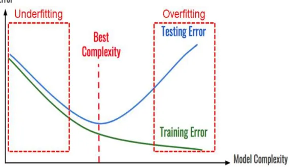
layers (e.g., input layer, hidden layer, and output layer) and the number of node of each layer (e.g.,f1(e), f2(e), f3(e) etc.). In addition, this part can control the degree of training depending on the number of layers and the number of nodes, and excessive layer number and node can cause overfitting problem of ANN algorithm. As the number of layers and nodes increases, the complexity of the algorithm model increases, overfitting and directly contributing to the problem, as shown in the figure below [1, 7].
Fig. 2.4. Example of algorithm inside compute node.
On the contrary, if the number of layers and nodes are set smaller than the required values, there will be many errors in the ML system as the underfitting problem will occur and ANN algorithm will not be able to train sufficiently.
As shown in the following graph, the underfitting problem and the overfitting problem may occur according to the number of layers and nodes of the ANN. Therefore, an optimized model structure is required and a number of optimized iterative training is required.
Fig. 2.5. Error rate change according to algorithm complexity. Optimize model complexity by comparing underfitting and overfitting conditions.
Therefore, the number of layers and nodes in 1: 3: 1 (Input layer: Hidden layer: Output layer) proposed in this paper are set considering the optimal complexity without problems of underfitting and overfitting.
3) Forward-propagation model: In this paper, forward learning is performed using the Rectified Linear Unit (ReLU (x) = max (0, x)) model.
4) Back-propagation model: Calculate the mean squared error (MSE) loss between the model's output data and the TCAD simulation data, and use the optimized model with the
stochastic gradient descent (SGD) method and The Adaptive Moment Estimation (ADAM) method.
Based on the above conditions, our group can design a basic ANN algorithm structure and use the data extracted through TCAD simulation to train the ML system. Figure 2.6 shows an example analysis of the effects of variability effect used in this study. The setup algorithm shows the process by which the variability source variable data entered through the activation function is simultaneously propagated to each next node and back to the previous node through the inverse correction function through error calculation. Inverse correction process during one epoch in this paper, the number of iterations (epoch) is repeated more than 20,000 times. Therefore, the error between the data output through the ANN algorithm(Y1: YN) and the determined TCAD simulation data(G1: GN) is calculated through the MSELOSS function in each forward and backward training process repeated during the training process. As a result, iterative training of the ANN algorithm ends when sufficient training is in progress (the error converges to 1% or less between the algorithm output value Y1: YN and the TCAD simulation result value G1:
GN). Therefore, the output value of well-training algorithm form a characteristic distribution similar to the TCAD simulation data [1, 7].
Fig. 2.6. Training schematic of artificial neural network algorithm.
The input and output data used in the ANN algorithm and the TCAD simulation can be described sequentially through the following algorithm application steps:
Fig. 2.7. The machine learning algorithm training procedures.
First, set up the basic algorithm structure and internal functions of the ANN algorithm.
The training input/output data is extracted by TCAD simulation for training the ANN algorithm. In the training data extraction phase, the model trains the same value that were
input to the TCAD simulation. Therefore, the trained ANN algorithm adjusts the internal model based on the input and output data obtained from the TCAD simulation. In the optimization phase of the following algorithm, the output values of the ANN algorithm and the TCAD simulation are compared to adjust the weight of the internal function.
Once the training algorithm is sufficiently completed (TCAD simulation data and error rate < 1%), the ANN algorithm is validated through the independently extracted test data.
As for the verification result, the accuracy is determined by extracting the characteristic change data (output data for testing) corresponding to the implementation data (input data for testing) of the variability sources. In particular, in the verification process with test data, independent data is used rather than input/output data used in training. Therefore, it inserts new variable input data that has not been previously validated (not extracted by TCAD simulation) into the TCAD simulation and ANN algorithms simultaneously. After comparing the output values of the TCAD simulation and the ANN algorithm, the error rates of the two approaches are determined [8, 9].
The training and testing procedure of the ANN algorithm are performed as described above, and the input and output data used at each step are extracted and verified through the TCAD simulation. Therefore, the ANN algorithm training and testing method based on TCAD simulation should be considered as follows:
1) Quantitative preprocessing of input and output data.
Preprocessing of the data is required when the data used to train and test the ANN algorithm is extracted by TCAD simulation. TCAD simulation data that has not been
preprocessed is not suitable data type to enter the ANN algorithm. For TCAD simulations that use the 3D Stochastic Model to implement variability sources, the direct input of variability parameters is restricted. For example, to set the effect of WFV on TiN metal materials, we can perform TCAD simulations by providing arbitrary parameters (e.g., metal crystal generation seed, average metal crystal size, crystal distribution standard deviation, etc.) through an internal model. Therefore, <111> orientation and the <200>
orientation metal grains are generated on the surface of the metal and the oxide.
However, the parameters provided through TCAD simulation are not suitable as input/output data sets for training ANN algorithms. This is because data for training and testing ANN algorithms must consist of input and output data matrices of the same dimension. For example, if 1000 threshold voltage distribution is the output values, we need 1000 input values. Therefore, the input values of the variability source used in this study are the internal functions provided by the TCAD simulation, as well as the method of declaring arbitrary variables created in Python as external variables in the TCAD simulation.
2) Accuracy of TCAD simulation.
The comparison of ANN algorithms proposed in this paper is the predictive data of the effects of variability sources through TCAD simulation. Therefore, before applying the ANN algorithm, it is important that the analysis of the effects of the variability sources through the TCAD simulation is consistent with measurement results. Unfortunately, the results of all the variability sources presented in this paper are based on input and output
values through TCAD simulation and do not include actual measured data. However, based on the results of previous studies, the effect of variability sources through TCAD simulations are expected to be similar to actual device measurement results. Sections 3 and 4 of this study describe in more detail how to calibrate TCAD simulations and measurement data.
As a result, in this study, we optimize the ML approach to efficiently predict/analyze the various conditions above. Therefore, we have proposed an ML model that shows the same accuracy and fast predictability as the TCAD simulation.
2.4 Summary
To design an ML system that interoperates with TCAD simulation, it is important to develop detailed design and mapping technology inside the system to efficiently use the extracted input/output (I/O) training data. Therefore, in this paper, we focuses on the following four factors to develop the mapping technology of ML system.
1. Optimize the number of I/O data. Since I / O data is extracted using TCAD-based simulation and is directly related to the efficiency of the entire system, it is very important to find the optimal number of data considering the calculation cost.
2. Optimization of the number and number of hidden layers. For artificial neural network (ANN) -based algorithms, the number of computational nodes and the number of layers present in them are important factors in determining the complexity and accuracy of the overall algorithm. So the goal is to develop the optimal detailed design to reach the target accuracy.
3. Selection of forward calculation model and backward correction model. The basic operation mechanism of Artificial Neural Network (ANN), requires the selection of a forward computational model and a backward correction model as internal computational functions in order to represent an accurate predicted output value at an input value. The contents of internal functions differ depending on the purpose of use, so it is important to set clear goals for analysis and set the most efficient model.
4. Optimization of the number of training. For ML system, the more accurate the
training is, the more accurate the system. However, excessive iterative training can increase the computational cost of the system and can cause problems like vibration of the predicted output value, so the goal is to set the optimal number of iterations.
As a result, this study is divided into [Identify-Analysis-Interlock] step for extracting training data by TCAD simulation. We also propose an ML system based on the variability source analysis system that consumes optimal computational costs and accommodates the accuracy and integration of commercial tools.
References
[1] V. Subramanian, Deep Learning with Pytorch, 1st ed. iG Publishing Pte. Ltd. Press, 2018.
[2] ITRS, Denver, CO, USA. International Technology Roadmap for Semiconductors(ITRS), 2015. Online(http://www.itrs2.net/).
[3] Sentaurus Device User Guide Version: K_2015.06, Synopsys, Mountatin View, CA, USA, Jun. 2015.
[4] K. Ko, J. K. Lee, M. Kang, J. Jeon, and H. Shin, “Prediction of Process Variation Effect for Ultrascaled GAA Vertical FET Devices Using a Machine Learning Approach”
IEEE Trans. Electron Devices, Vol. 66, No.10, pp. 4474-4477 Sep. 2019, doi:
10.1109/TED.2019.2937786
[5] V. Janakiraman, A. Bharadwaj, and V. Visvanathan, “Voltage and Temperature Aware Statistical Leakage,” IEEE Trans. Computer-Aided Design of Integrated Circuits and Systems, Vol. 29, No. 7, pp. 1056-1069, Jul. 2010, doi: 10.1109/TCAD.2010.2049059 [6] J. Virarahgavan, S. J. Pandharpure, and J. Watts, “Statistical Compact Model Extraction:,” IEEE Trans. Computer-Aided Design of Integrated Circuits and Systems, Vol. 31, No. 12, pp. 1920-1924, Dec. 2012, doi: 10.1109/TCAD.2012.2207955
[7] G. W. Burr, R. M. Shelby, S. Sidler, C. D. Nolfo, J. Jang, I. Boybat, R. S. Shenoy, P.
Narayanan, K. Virwani, E. U. Giacometti, B. N. Kurdi, and H. Hwang, “Experimental Demonstration and Tolerancing of a Large-Scale Neural Network (165 000 Synapses),”
IEEE Trans. Electron Devices, Vol. 62, No.11, pp. 3498-3507, Nov. 2015, doi:
10.1109/TED.2015.2439635
[8] M. Abe, T. Nakamura, and K. Takeuchi, “Pre-shipment Data-retention/ Read-disturb Lifetime Prediction & Aftermarket Cell Error,” in Proc. Symp. VLSI Technol., pp. T216- T217, Jun. 2019, doi: 10.23919/VLS IT.2019.8776480.
[9] T. Ohashi, A. Yamaguchi, K. Hasumi, M. Ikota, G. Lorusso, C. L. Tan, G. V. D. Bosch, and A. Furnemont, “Precise measurement of thin-film thickness in 3D-NAND device with CD-SEM” Journal of Micro/Nanolithography MEMS and MOEMS, Vol. 17, No. 2, May. 2019, doi: 10.1117/1.JMM.17.2.024002
Chapter 3
Prediction of Process Variation Effect for Ultra- scaled GAA Vertical FET Devices
In this section, we present an accurate and efficient ML approach which predicts variations in key electrical parameters using PV from ultra-scaled GAA VFET devices.
The 3D stochastic TCAD simulation is the most powerful tool for analyzing process variations, but for ultra-scaled devices, the computation cost is too high because this method requires a simultaneous analysis of various sources. The proposed machine- learning approach is a new method which predicts the effects of the variability sources of ultra-scaled devices. It also shows the same degree of accuracy as well as improved efficiency compared to a 3D stochastic TCAD simulation. An ANN-based ML algorithm can make MIMO predictions very effectively and uses an internal algorithm structure that is improved relative to existing techniques to capture the effects of process variations accurately. This algorithm incurs approximately 16% of the computation cost by predicting the effects of process variability sources with less than 1% error compared to a 3D stochastic TCAD simulation.
3.1 Introduction
Over the past four decades in the electronics industry, the typical size of an electronic device has been aggressively reduced to achieve higher levels of performance and efficiency, in keeping with Moore’s law. Meanwhile, the aggressive trend of ultra-scaling the device size for integration is leading to unexpected problems, such as process variability issues. The major variability sources, including LV and GV sources, have been widely studied in relation to both planar and GAA devices [1-4]. In the case of LV sources, work-function variation (WFV) effects in high-k/metal gate (HK/MG) devices, which is noted as the most important statistical variability sources, should be considered to cope with a critical risk of device performance due to randomly occupied grain- orientation of gate metal [5, 8, 10]. Moreover, in the case of GV sources, the effect of CD variation is the most influential variability sources in varying the performance of the devices, and as the device size decreases, this effect can no longer be ignored. In earlier work, depending on the technology node, the structure of the device could change from the planar to the GAA type through the use of FinFET devices, and variability sources with dominant effects existed independently in each generation [6, 7]. However, in subsequent generations of transistors, the effects of all variability sources should be analyzed concurrently, as opposed to focusing on the key sources, for accurate predictions of the correlations for each source.
To analyze simultaneous variability in ultra-scaled devices, the 3D stochastic TCAD simulation has been proven to be superior in various studies as a leading analytical platform [3, 4]. However, as the number of variability sources to be considered increases, an analysis of a large number of sample devices is required. Therefore, a high computational cost is inevitable for accurate predictions. In recent studies, variability analysis methods with low computation overhead were proposed based on compact modeling for analysis of circuit level as well as device level, but overall this approach still has a high error rate because it is based on many preconditions for simplification of the formulae used [8-11]. Therefore, we propose a new variability analysis method based on a ML algorithm with accuracy that matches that of the 3D stochastic TCAD simulation in an ultra-scaled device and with improved calculation efficiency at the device level.
3.2 Simulation Structure and Methodology
The 3D TCAD simulation was performed using Synopsys Sentaurus, which was carefully calibrated with the experimental data of 5-nm 3stacked NP FET by referring to the reference [12]. To capture the transport characteristics of nanoscale devices, ballistic transport was considered, and the drift-diffusion (DD) approximation was used for carrier transport [13]. The saturated velocity and a ballistic model were carefully adjusted to match the experimental data. The interfacial mobility degradation was modeled using the Lombardi method, and a thin-layer mobility model was included to account for the thin channel thickness. In addition, the quantum effect caused by the small structure of the device is considered, and the contact resistivity, which has a large influence on the current as the device size is reduced, is set to 3 × 10⁻⁹Ω/cm2by referring to the reference [14].
Fig. 3.1 (b)-(c) shows the 3D structures of a NW VFET and a NP VFET, indicating the random distribution of metal grains on the HK/MG interface area, as noted in the TCAD simulation. The nominal device parameters are based on the International Technology Road Map for Semiconductors (ITRS) for 4/3 nm node technology low-power transistors, including a physical gate length (Lg) of 12 nm, an equivalent oxide thickness (EOT) of 0.6 nm, a nanowire diameter (dNW) and channel thickness (Tch) of 5 nm, channel width (Wch) of 40 nm, a supply voltage (Vdd) of 0.55 V.
Table 3.1 shows the quantitative values of the variability considered in this paper.
Fig. 3.1. (a) Calibration of the TCAD models with the experimental data of 5-nm node three stacked NP FET (b) Structure of NW VFET. (c) NP VFET.
In order to implement CD variation, the variation of Lg, Tch is assumed to be identical Gaussian distributions of 3σ=1 nm(critical dimension control). The variation of EOT is assumed to be 4% at 3σ [17]. In addition, the material of the metal gate is TiN, and the grain size (GS) set to 10 nm. The work function variation is implemented in random devices using Metal Work Function Variation (3D Stochastic WFV Model). Then, the electrical characteristics (Id-Vg plot) of the device were directly sampled through the TCAD Sentaurus workbench to extract the key electrical parameters caused by the WFV and CD variations. The key electrical parameters of the random device are extracted from approximately 1000 Id-Vg plot samples and are based on data that implements the individual dimensions of each device.
Table. 3.1. Summary of the process variability sources parameters.
3.3 Results and Discussion
Figure 3.2 shows the basic structure of a MIMO ANN. The ANN algorithm structure has five layers, referred to as the input, first hidden, second hidden, third hidden, and the output layers. Each hidden layer that receives input layer data returns a calculated value to the output layer. For accurate process variation training, a rectified linear unit (RELU) activation function is used to prevent the vanishing gradient problem, which can arise due to the complexity of the algorithm. The ANN-based ML algorithm was trained using the PyTorch python library.
Fig. 3.2. MIMO artificial neural network structure. All input/output (I/O) values include the source of the process variation and the dimensions of the device and represent corresponding key electrical parameters.
Table. 3.2. Multi-Input Multi-Output ANN Algorithm.
1) WIis 5 × 30 input weight matrix and BIis a 30× 1 bias vector 2) WH1,2is 30 × 30 input weight matrix and BH1,2is a 30× 1 bias vector 3) WOis a 5×30 output weight matrix and BOis a 5×1 bias vector
4) (WI, BI), (WH1,2, BH1,2), (WO, BO) are unknown variables and are obtained during the trainging phase.
5) φ(x) is the activation function : Relu 6) P is a input vector (Variability parameters).
The weight value(WI, WH1, WH2, WO) assigned to each computation node and the vector value(BI, BH1, BH2, BO) that determines the computation direction are unspecified
variables and are constantly modified in the training phase. Therefore, the input and output values are calculated as a simple function, as shown in Figure 3.2. This calculation process is repeated approximately 20,000 times or more and the calculation runs in a form similar to the Taylor series to return an accurate final value [15, 16].
The input values inserted in the ANN algorithm include the work function variation value due to the WFV effect and the various values of Lg, Tch, and EOT due to the CD Variation. In addition, it contains the constant parameters of the specified device to learn various dimensions of the device. Therefore, although the structure of the device is different through single learning, it is possible to confirm the influence of the variability source in the NP VFET structure as well as the NW VFET. In addition, for the independent algorithm learning environment, the algorithm learns arbitrary values that are not related to the device specification presented above. The algorithm presented in this paper refers to the learned values of the GAA VFET device in the 6/5nm technology node [17]. The weights and vectors within the learned algorithm are used to determine the variability of the NW VFET and NP VFET test devices.
Figure 3.3 shows the TCAD simulation results to be learned and tested in the ANN algorithm for 1000 NW VFET and NP VFET device samples. The effect of the variability sources is larger in NW VFETs with relatively small channel area. This tendency is trained through the various input parameters of the ML approach mentioned above.
Fig. 3.3. Id-Vg plots for 1000 samples of (a) NW VFET and (b) NP VFET devices with all the variability sources.
Figure 3.4, 3.5 and 3.6 shows the distributions and the correlations between the key electrical parameter variations obtained from the 3D stochastic TCAD simulations and from the ANN-based ML algorithm. Both sets of distributions and correlations, including the effect of WFV and the effect of CD variations (i.e., ∆Lg, ∆Tch, and ∆EOT), achieve a good match between the TCAD data and the extracted ML data. In addition, the radar chart of the two approach shows that the rate of error is close to nil for all key electrical parameter variations. In the device specification of the same dimension, in the case of NP VFET structure, the influence of WFV is decreased due to the increase of the gate area, and the influence of CD variation is increased due to the decrease of the gate controllability, compared to the NW VFET. The change of the electrical characteristics by the WFV is a source that directly changes the threshold voltage of the device, so it does not affect the SS characteristic. Therefore, the correlations between SS and other performance characteristics are low for the NW VFET devices where the influence of WFV is dominant. However, for NP VFET devices with increased CD variation effects, there is a significant correlation between SS and other performance characteristics. As a result, the effect of the variability sources can be different depending on the structural characteristics of the device, and it can be confirmed that these differences are accurately predicted in the analysis through the machine learning algorithm.
Fig. 3.4. Radar chart of the variation in key electrical parameters caused by WFV and GV sources (normalized by TCAD variations) of (a) NW VFET and (b) NP VFET.
Fig. 3.5. Comparison of scatter plots and correlations of the key electrical parameters between the TCAD data and the ML Approach results from NW VFET. The Quantile- Quantile plots of the key electrical parameters are plotted in the diagonal subfigures.
Fig. 3.6. Comparison of scatter plots and correlations of the key electrical parameters between the TCAD data and the ML Approach results from NP VFET. The Quantile- Quantile plots of the key electrical parameters are plotted in the diagonal subfigures.
The steps below are used for the quantitative extraction of the computation cost. The total computational cost of the ML approach for the analysis of process variability is determined by the sum of the amount of I/O data acquired for the training and the training and testing times of the internal algorithm. Therefore, in order to calculate the quantitative calculation cost compared to that of the TCAD simulation, the following three steps can be considered:
Fig. 3.7. Extract the minimum data amount to extract the effective distribution of the electrical characteristics
In the first step, the number of random devices samples required statistically is determined when analyzing the TCAD simulation independently. The variability sources used in this paper is the Gaussian distribution, which arbitrarily transforms the physical parameters of the device. Therefore, in order to understand the change in the characteristics of the device caused by such variability sources, a sufficient number of
random devices are required to form such a characteristic change as a Gaussian distribution. As a result, as shown in Step 1 of Fig. 3.7, when analyzing the characteristic change in about 600 or more random devices, it can be seen that the standard deviation converges to a certain Gaussian distribution. In other words, to analyze statistically the variability source, at least 600 TCAD simulation device analysis should be preceded. In this process, we can calculate the computational cost for analyzing the impact of variability using TCAD simulation.
Fig. 3.8. Extract the training data amount of ML Approach to ensure the same level of accuracy as the TCAD simulation.
In the second step, the minimum number of random device samples for learning ANN algorithm through TCAD simulation data is grasped. In the first phase, a TCAD simulation required samples of at least 600 random devices to statistically analyze the variability. However, the ANN algorithm shows that sufficient prediction is possible with
fewer random device samples than the TCAD simulation. The number of minimum random device samples for learning the ANN algorithm presented in this paper is about 100. In this process, a random device sample of the TCAD simulation for training and testing exists independently. The number of random device samples for training is gradually increased. After the training, the ANN algorithm model extracts the error rate by comparing it with about 1000 random sample samples for the test. As a result, the analysis of the influence of the variability sources through the ANN algorithm requires about 6 times fewer random device samples than the TCAD method. Therefore, it is possible to quantitatively estimate the reduction in the computational cost of the ANN algorithm when the error of the two approaches is less than 1%.
Fig. 3.9. Training and calculation time extraction of ML Approach internal algorithm based on acquired training data.
In the third step, the number of learning iterations for training 100 ANNs of random
device samples claimed in the previous step is shown. In the following procedure, we show the error with testing data (1000 random device samples for testing) according to the number of learning iterations of the ANN algorithm learned through training data (100 random device samples for learning). In the same way as above, the training data and the testing data exist independently and are extracted through TCAD simulation. As a result, the number of training iterations shows an effective reduction of the error rate when it is performed about 20,000 times or more.
Fig. 3.10. Schematic diagram of total calculation cost.
Therefore, considering the total computational cost, the ML approach is nearly six times faster than the TCAD simulation, as shown in figure 3.10. The error rate of the key electrical parameter variation is trained to be less than 1% on average, as shown in Table 3.3.
Table 3.3. Comparison of the computation cost and accuracy of ML approach and TCAD Simulation.
Compute Environment: Intel Xeon CPU E5-2687W 216 V2 (3.5 GHz × 16) processor with 128 GB of RAM
Stochastic approach (TCAD Simulation) takes about 0.83 h per single sample. Thus, analyzing 600 samples takes about 500 h. ML approach (MINO ANN Algorithm), it takes about 83.33 h to obtain minimum training data and calculate test data. In the ML approach compared to TCAD, the computational cost can be reduced by about 83%.
3.4 Summary
In this section, we proposed a new analytical method based on an ANN-based ML algorithm to assess the degree of process variability in ultra-scaled devices. According to previous studies, 3D stochastic TCAD simulations are considered to be the most powerful means of analyzing process variation. However, for an analysis of ultra-scaled devices, various process variation sources must be analyzed simultaneously and integrally.
Therefore, existing methods require too expensive computation cost for accurate prediction. Therefore, analyzing the process variation sources using the ANN-based ML approach can significantly improve (6×) the calculation efficiency while maintaining the high accuracy (relative error of approximately 1%) of the existing 3D stochastic TCAD simulation. As a result, the method of analyzing process variability levels proposed in this paper can provide useful guidelines to those who develop and design ultra-scaled devices.
References
[1] X. Wang et al, “FinFET Centric Variability-Aware Compact Model Extraction” IEEE Trans. Electron Devices, vol. 62, no. 10, pp. 3139-3146, Oct. 2015, doi:
10.1109/TED.2015.2463073
[2] F. A. Lema et al, “Comprehensive ’Atomistic’ Simulation of Statistical Variability, and Reliability in 14 nm Generation FinFETs” in proc. IEEE SISPAD, pp. 157-160, Sep.
2015, doi: 10.1109/SISPAD.2015.7292283
[3] X. Wang, B. Cheng, A. R. Brown, C. Millar, J. B. Kuang, S. Nassif, and A. Asenov,
“Interplay Between Process-Induced and Statistical,” IEEE Trans. Electron Devices, vol.
60, no. 8, pp. 2485-2492, Aug. 2013, doi: 0.1109/TED.2013.2267745
[4] L. Gerrer et al, “Interplay Between Statistical Reliability and Variability, ” in Proc.
IRPS, Jun. 2013, pp. 3A.2.1-3A.2.5, doi: 10.1109/IRPS.2013.6531972
[5] X. Wang, A. R. Brown, B. Cheng, and A. Asenov, “Statistical variability and reliability in nanoscale FinFETs” in Proc. IEEE Int. Electron Devices Meeting, Dec. 2011, pp. 5.4.1-5.4.4, doi: 10.1109/IEDM.2011.6131494
[6] T. H. Bao et al, “A Comprehensive Benchmark and Optimization of 5-nm Lateral and Vertical GAA 6T-SRAMs” IEEE Trans. Electron Devices, vol. 63, no. 2, pp. 643-652, Feb. 2016, doi: 10.1109/TED.2015.2504729
[7] V. Moroz, “Transistor and Logic Design for 5nm Technology Node” Synopsys Silicon to Software, Semicon Taiwan , Sep. 2016
[8] H. Dadgour, K. Endo, V. K. De, and K. Banerjee “Grain-Orientation Induced Work Function Variation in Nanoscale Metal-Gate Transistors—Part I,” IEEE Trans. Electron Devices, vol. 57, no. 10, pp. 2504-2514 Oct. 2010, doi: 10.1109/TED.2010.2063191 [9] P. H. Vardhan, S. Mittal, S. Ganguly, and U. Ganguly, “Analytical Estimation of Threshold Voltage,” IEEE Trans. Electron Devices, vol. 64, no.8, pp. 3071-3077 Aug.
2017, doi: 10.1109/TED.2017.2712763
[10] K. Ko, M. Kang, J. Jeon, and H. Shin, “Compact Model Strategy of Metal-Gate,”
IEEE Trans. Electron Devices, vol. 66, no.3, pp. 1613-1617 Mar. 2019, doi:
10.1109/TED.2019.2891677
[11] X. Jiang, X. Wang, R. Wang, B. Cheng, A. Asenov, and R. Huang, “Predictive compact modeling of random variations in FinFET technology for 16/14nm node and beyond” ” in Proc. IEEE Int. Electron Devices Meeting, Dec. 2016, pp. 28.3.1-28.3.4, doi: 10.1109/IEDM.2015.7409787
[12] N. Loubet et al., “Stacked nanosheet gate-all-around transistor to enable scaling beyond FinFET,” in Proc. Symp. VLSI Technol., Jun. 2017, pp. T230–T231, doi:
10.23919/VLSIT.2017.7998183.
[13] J. D. Bude, “MOSFET modeling into the ballistic regime,” in Proc. IEEE SISPAD, Sep. 2000, pp. 23–26, doi: 10.1109/SISPAD.2000.871197.
[14] P. Adusumilli et al., “Ti and NiPt/Ti liner silicide contacts for advanced technologies,” in Proc. IEEE Symp. VLSI Technol., Jun. 2016, pp. 1–2.
[15] J. Virarahgavan, S. J. Pandharpure, and J. Watts, “Statistical Compact Model
Extraction:,” IEEE Trans. Computer-Aided Design of Integrated Circuits and Systems, Vol. 31, No. 12, pp. 1920-1924, Dec. 2012, doi: 10.1109/TCAD.2012.2207955
[16] V. Subramanian, Deep Learning with Pytorch, 1st ed. iG Publishing Pte. Ltd. Press, 2018.
[17] ITRS, Denver, CO, USA. International Technology Roadmap for Semiconductors(ITRS), 2015. Online(http://www.itrs2.net/).
Chapter 4
Prediction of Process Variation Effect for 3D NAND Flash Memories
In this section, we propose a variability-aware ML approach that predicts variations in the key electrical parameters of 3D NAND Flash memories. For the first time, we have verified the accuracy, efficiency, and generality of the predictive impact factor effects of ANN algorithm-based ML systems. ANN-based ML algorithms can be very effective in MIMO prediction. Therefo