An indirect time-of-flight sensor with adaptive pixel background light suppression based on the delta-sigma technique. The principle of time-of-flight (ToF) is the measurement of distance based on the time difference between the transmitted and reflected light waves.
Introduction
Range detection methods overview
- Triangulation
- Interferometry
- Time-of-Flight
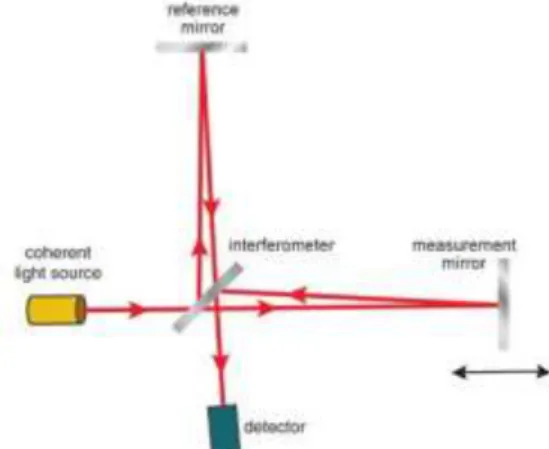
In Figure 1.2, a coherent light source emits light to a mirror, and the reflected light passes through an interferometer and is reflected back to the reference mirror and enters the detector. The first thing is that the complexity of this system is very high and the second thing is that the maximum detection range is limited. Time-of-Flight is a range detection system by measuring the return time of emitted light.
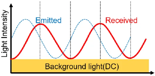
If the signal is sampled only once, it is impossible to distinguish the intensity of the light due to several reasons such as phase movement, reflectivity due to the color or surface features of the object, and the background. The depth information of the target is wrong depending on the phase of the signal.
Range detection error by Background light
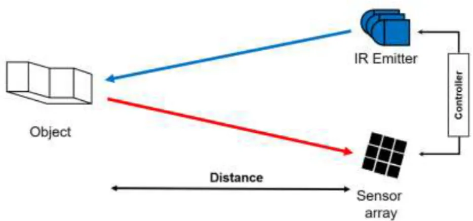
Time-of-Flight 3D Imaging
Principles of Time-of-Flight 3D Imaging
- Classification of Time-of-Flight
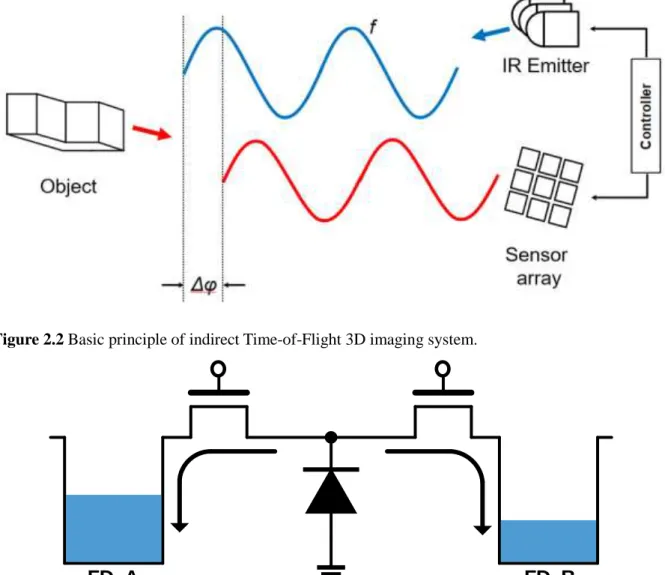
- Distance detection by phase difference between emitted and reflected light
Correlation between background light and depth image
Conceptual ideas of background light suppression
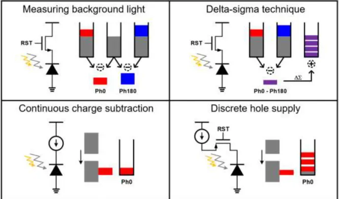
If there is a lot of background light and the signal is saturated by background light, the sensor cannot measure the phase difference. Background light is a DC signal, so BL added to the out-of-phase signal is the same as BL added to the in-phase signal. The first method is to measure background light and subtract the same value from the in-phase signal and the out-of-phase signal.
The second method is the delta-sigma technique which subtracts the in-phase value from the out-of-phase value. There are 4 types of implementing delta integrators; Flipping photodiode, Flipping capacitor, Flipping CDS operation and cross-coupled capacitor. It samples photocurrent through background light and then only accumulates additional photocurrent, except the continuously flowing current through BL.
Previous BLS techniques in iToF depth sensor
- Measuring background light and subtraction scheme
- Delta-Sigma background light suppression scheme
- Flipping photodiode
- Flipping input capacitor
- Flipping CDS operation
- Continuous charge subtraction scheme
- Sampling photocurrent by background
- Flipping feedback capacitor to delta accumulation
- Discrete hole supply scheme
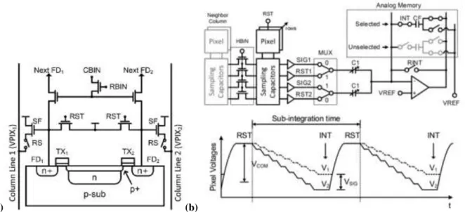
Each pixel has a capacitive trans-impedance amplifier (CTIA) to convert current to voltage. Nevertheless, to sample light-generated electrons into the integrating capacitor, switching may cause charge injection and is therefore not suitable for high-frequency operation [7]. Then, turning on the BWD switch integrates the charge for the BL+IR signal, but its sign is negative.
The in-phase signal is read in column row 1 and the out-of-phase signal is read in column row 2 and then connected to the mux connected to the CDS input capacitors in parallel with the column. In the first stage (the mux value is zero), SIG1 and RST2 are connected to the left node of the input capacitor, and then RST1 and SIG2 are connected in series after the mux value is high. In this case, the charge for the voltage difference at the left node of the input capacitor is sampled in capacitor 𝐶2.
Output voltage is voltage difference between in-phase signal + BL and out-of-phase signal + BL. In Figure 3.6 (b), CS&H detects DC current by setting S/H to high state and gate-source voltage of 𝑇1 is defined. After S/H transistor turns off, gate-source voltage remains conserved by CS&H, thus facilitating BL suppression [10].
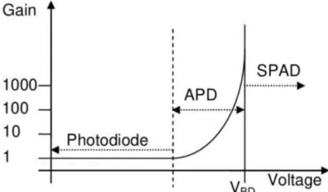
In Figure 3.7, a low noise APD is implemented with a p-well/DNW transition and it has better sensitivity, but an additional p-sub guard ring is needed to prevent premature degradation, so the pixel pitch is quite large due to the photodiode structure. Coarse is inverting the integration capacitor and fine is sampling only BL and canceling the photocurrent through BL. In Figure 3.8, photocurrent is generated only by BL in the initial state and then copied by the current mirror.
In Figure 3.9, three-transistor discrete-time charge sources (ALC1, Valc, ALC2) are implemented for ambient light cancellation. The electrons in the FD junction recombine with discrete hole packing and this helps saturation of the FD junction and prevents depth errors from ambient light.
Proposed i-ToF sensor with in-pixel Adaptable BLS based on ΔΣ
Solution of previous work problem
- Adaptable ΔΣ by monitoring FD node
- Automatic TX chopping interlocking adaptable ΔΣ
- Pinned-PD for accelerating charge transfer
- In-pixel integrator for global ΔΣ operation
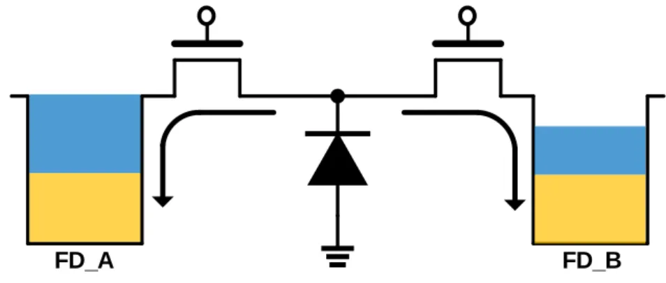
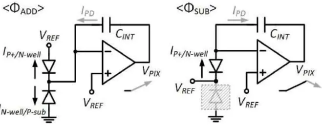
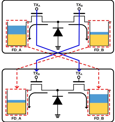
In addition phase both P+/N-well PD and N-well/P-sub PD photocurrent, but in subtraction phase only P+/N-well PD photocurrent. If TX strength is different, charges generated on PD are transferred to FD capacitors differently over in-phase case and out-of-phase case. After ΔΣ operation, T flip flop for TX chopping controls that TX signals are inverted and collect in-phase signal on FD B node and out-of-phase signal on FD A node.
The third problem is only possible in low-frequency operation due to the conventional characteristic of the photodiode structure. To be able to use high modulation frequency up to 50 MHz, a pinned dopant gradient photodiode is proposed. In Figure 4.3 (a), conventional PD has a flat electric field from PD to FD node, so as the frequency increases, electrons generated on PD cannot be fully transferred to the FD node for a certain time.
By the gradient doping concentration in the photodiode region, a steep electric field is generated from the PD to the FD node and helps the electrons to be fully transferred to the FD node [14]. Through the split integrator, the pixel pitch can be decreased because there is no integrator in the pixel, so it is effective in terms of pixel resolution. Therefore, the ΔΣ time is much longer than the global ΔΣ operation and cannot implement many subintegrations.
In this case, the ΔΣ time is very short, so it can implement many times ΔΣ compared to column level ΔΣ.
Proposed Sensor Design
- Proposed overall architecture
- In-Pixel Background Light Suppression (BL) structure
- Smart reset technique for low charge-injection
- TX gate signal chopping in pixel-level for reducing mismatch
- Overall operation
By monitoring the FD node voltage through the inverter-based comparator, it determines whether to enable or disable delta-sigma operation between FD node A (in phase) and FD node B (out of phase). At the time of subintegration, the reset of the FD node is automatically implemented by transferring the charge of the FD node to the integration capacitor. Usually, the signal for 0 degrees and 90 degrees is collected at the FD node A and the signal for 180 degrees and 270 degrees is collected at the FD node B.
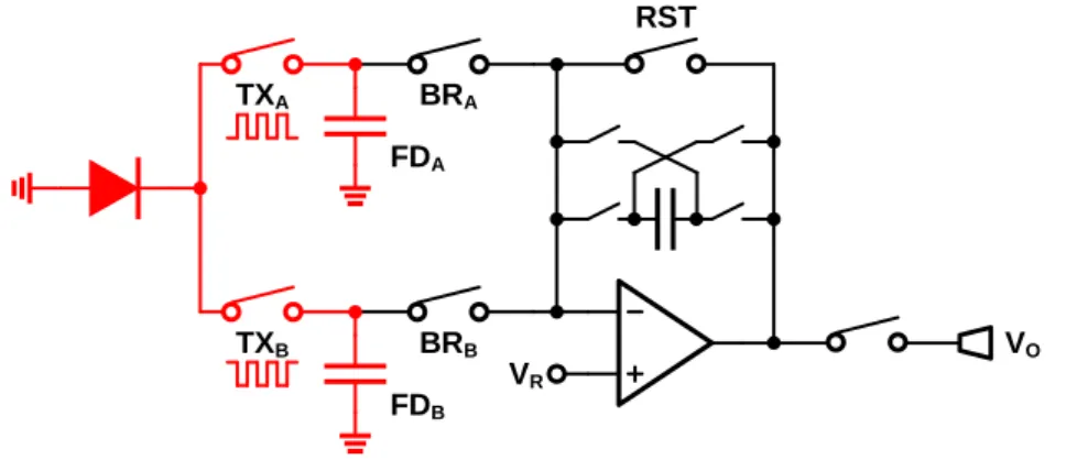
In the BLS phase, by turning on the BR A switch, the charge of the FD A node switches to the ratio of the integrating capacitor and the capacitor × voltage corresponding to the signal 1, and the background light is added to the reference voltage. Then, by turning on the switch BR B, the integration capacitor is rotated and charged at the node FD B in the integration capacitor. However, in this case, the voltage for signal 2 and the background light is reduced because the capacitor is reversed.
Through the delta-sigma node of the FD, we can get the difference signal between the in-phase signal and the out-of-phase signal, excluding the background light. A smart adaptive ΔΣ controller scheme is proposed to reduce unnecessary switching noise when the background light is not dominant. In Figure 4.8, a converter-based comparator monitors the light state, and the converter's latch memory stores this data for the delta-sigma phase.
If the FD voltage is below 1.6V (high light), the converter output is high and determines the delta-sigma and reset of the FD node. In the next phase, the comparator again monitors the FD node and if the FD voltage is below 1.6 V, it determines delta-sigma operation. After ΔΣ operation, the in-phase signal is stored on FD B and the out-of-phase signal is stored on FD A.
Therefore, charges from in-phase signal on FD B are first transferred to integration capacitor and charges from FD A are transferred to reverse integration capacitor. At the next sub-integration stage, TX heel signal is inverted again, so in-phase signal is stored on FD A and out-of-phase signal is stored on FD B node. Through these techniques, it can reduce unnecessary switching noise or charge injection when light signal is not high and it can compensate storage node mismatch and TX strength mismatch problem by process variation.
Measurement result
- Measurement system setup
- Light source and optical emitter design
- Light source - LED
- Light source – LD
- Light source device comparison
- Switching topology
- LD board measurement
- Chip measurement
- Conclusion
In Figure 5.4, to literally get a stimulated emission, it needs two mirrors for the resonant cavity and plays the role of light amplification. In this case it has the disadvantage that the impedance of the drain node of the switch becomes infinite when the switch is turned off. The difference between the in-phase signal and the out-of-phase signal is about -0.057V and the closed loop gain is about 0.4.
The difference between the in-phase signal and the out-of-phase signal is approximately 0V and the closed-loop gain is approximately 0.4. After ΔΣ operation, the pixel output voltage is constantly 1.998 V because the voltage increase from the in-phase signal is the same as the voltage decrease from the out-of-phase signal. The difference between the in-phase signal and the out-of-phase signal is approximately 0.053V and the closed-loop gain is approximately 0.4.
In this research, a 92 × 72 i-ToF with smart adaptive background light attenuation based on ΔΣ techniques is proposed. Second, to compensate for the mismatch problem with process variation, pixel-level automatic chopping is proposed. Finally, for high frame rate and high background suppression performance, all pixels include individual in-pixel integrators and simultaneously perform the ΔΣ operation.
Turning off the in-pixel amplifier array on integration time is useful for power saving because integration time is dominant than readout time and reset time. Charbon, “Design and Characterization of a CMOS 3-D Image Sensor Based on Single-Photon Dumping Diodes,” IEEE J. Gasparini et al., “A 32×32-pixel time-resolved single-photon image sensor with 44.64 μm pitch and 19.48% fill factor with on-chip drive/frame skip features achieving 800 kHz sensing rate for quantum physics applications,” in IEEE ISSCC Dig.
Han, “A 413X240-Pixel Sub-Centimeter Resolution Time-of-Flight CMOS Image Sensor with In-Pixel Background Cancellation Using Lateral-Electric-Field Charge Modulators,” IEEE ISSCC Dig. Liao, "A CMOS Time-of-Flight Depth Image Sensor with In-Pixel Backlight Cancellation and Phase-Shifting Readout Technique," IEEE J. Stoppa, "A 160X120-Pixel Range Camera with In-Pixel Correlated Dual Sampling and Fixed Pattern Noise Correction," IEEE J .
Hofbauer, "High Dynamic Range Background Light Suppression for a TOF Distance Measurement Sensor in 180nm CMOS", IEEE SENSORS, Oct.2011. Chae, “A 64x64 APD-based ToF image sensor with backlight attenuation up to 200klx using In-Pixel Auto-reset and chopping”, IEEE Symp.