저작자표시-비영리-변경금지 2.0 대한민국 이용자는 아래의 조건을 따르는 경우에 한하여 자유롭게
l 이 저작물을 복제, 배포, 전송, 전시, 공연 및 방송할 수 있습니다. 다음과 같은 조건을 따라야 합니다:
l 귀하는, 이 저작물의 재이용이나 배포의 경우, 이 저작물에 적용된 이용허락조건 을 명확하게 나타내어야 합니다.
l 저작권자로부터 별도의 허가를 받으면 이러한 조건들은 적용되지 않습니다.
저작권법에 따른 이용자의 권리는 위의 내용에 의하여 영향을 받지 않습니다. 이것은 이용허락규약(Legal Code)을 이해하기 쉽게 요약한 것입니다.
Disclaimer
저작자표시. 귀하는 원저작자를 표시하여야 합니다.
비영리. 귀하는 이 저작물을 영리 목적으로 이용할 수 없습니다.
변경금지. 귀하는 이 저작물을 개작, 변형 또는 가공할 수 없습니다.
Abstract
Widespread energy harvesting, generating self-sufficient power from the surrounding environment, such as wind, solar and geothermal, have attracted increasing attention in the past decade due to the energy crisis and global warming. Among them, many technological devices converting mechanical energy into other forms of energy or vice versa have been proposed and investigated because of an extended life time, no recharging procedures, and their scalability.
Generally, mechanical energy converted into electricity, namely, by using electromagnetic, electrostatic, and piezoelectric effects. Among many technologies, energy harvesting technologies based on the piezoelectric effect, named as piezoelectric nanogenerators (PENG), have been extensively investigated because of an extended life time, no recharging procedures, and scalability. A high flexibility or stretchability is essential in generating high-power continuous electric output signals. The high flexibility can provide an opportunity applicable to a target object without any limitation of its shape and movement. Most recently, a new type of power generating device, named as triboelectric nanogenerator (TENG) based on triboelectric effects coupled with electrostatic effects have been demonstrated as powerful means of harvesting mechanical energy from living environment. In traditional TENGs, the two materials were chosen according to the difference in surface potentials, e.g., the polymer material (i.e. Teflon) terminated with the most electronegative functional group as the negative side and the low work function material (i.e. Al metal) as the positive side, apart from each other (named as airgap). When the two materials are contacted, the polymer material at the negative side tends to gain electrons from Al metal, resulting in being negative compared with Al. Thus, a key approach to improve the electrical output performance of the TENGs from the materials aspect is to increase the triboelectric surface charge density through material modification and surface functionalization. In this study, we introduce highly-ordered embossed
thin films with hollow hemispheres as one of promising structures for nanogenerators and pressure sensors, as well as extremely stable and directional anisotropic power generation in the composite- type piezoelectric nanogenerators without any treatment of electrical poling. For triboelectric nanogenerators, the material modifications such as the dielectric constant, the compressibility, and the surface potential in TENGs have focused. Additionally, the increased density of surface charges primary determined by the intrinsic properties of the specific materials and the effective means to enhance the output power of TENGs have proposed, which are critically important for improving the output performance of TENGs.
Contents
CHAPTER 1. INTRODUCTION ... 1
CHAPTER 2. THEORETICAL BACKGROUND AND MOTIVATION ... 5
2.1 Piezoelectricity ... 5
2.1.1 Introduction to piezoelectricity ... 5
2.1.2 Piezoelectric energy harvesting ... 6
2.2 Triboelectricity ... 9
2.2.1 Mechanism for contact charging and charge transfer ... 9
2.2.2 Triboelectric energy harvesting ... 10
CHAPTER 3. OBJECTIVE AND IDEAS... 14
3.1 Flexibility for stable output performance ... 14
3.2 Difference in work function between two materials for electron transfer ... 15
3.3 Dielectric constant of insulating layer for high surface charge density ... 18
CHAPTER 4. EXPERIMENTAL PROCEDURE ... 20
4.1 Embossed hollow hemispheres thin films ... 20
4.1.1 Pressure Sensor ... 20
4.1.2 Piezoelectric nanogenerator ... 21
4.2 Piezoelectric hemispheres with stretchable composite films ... 22
4.3 Highly ordered sponge structured films ... 25
4.4 Mesoporous Pores Impregnated with Au Nanoparticles ... 26
4.5 Measurement of electrical characteristics ... 28
4.6 Microstructural analysis ... 29
CHAPTER 5. RESULTS AND DISCUSSION ... 30
5.1 Highly responsive pressure sensor based on embossed hollow hemisphrere ... 30
5.1.1 Crystal characteristics ... 30
5.1.2 Output performance ... 32
5.1.3 Numerical analysis ... 33
5.1.4 Polarity test ... 33
5.2 Embossed hollow hemisphere-based piezoelectric nanogenerator ... 35
5.2.1 Output performance ... 35
5.2.2 Stacking method ... 35
5.3 Piezoelectric hemispheres with stretchable composite nanogenerator ... 38
5.3.1 Output performance ... 38
5.3.2 Numerical analysis ... 40
5.3.3 Mechanical test ... 42
5.3.4 Stacking method ... 43
5.3.5 Anisotropic output characteristics ... 44
5.4 Hydrophobic sponge structure-based triboelectric nanogenerator... 47
5.4.1 Microstructural analysis ... 47
5.4.2 Output performance ... 48
5.4.3 Stability test ... 51
5.4.4 Force-response capacitance change ... 55
5.4.5 Mechanical test ... 56
5.4.6 Numerical analysis ... 56
5.5 Au nanoparticles-embedded mesoporous triboelectric nanogenerator ... 58
5.5.1 Porosity-response compressibility ... 58
5.5.2 Output performance without airgap ... 60
5.5.3 Mechanical test ... 63
5.5.4 Output optimization ... 65
5.5.5 Porosity-response capacitance change ... 65
5.5.6 Numerical analysis ... 68
5.5.7 Output performance with airgap ... 71
5.6 Applications in self-powered devices ... 74
5.6.1 Motion sensor for health monitoring... 74
5.6.2 Hydrophobicity based humidity sensor ... 75
5.6.3 Shape mapping sensor for monitoring the local touching ... 78
5.6.4 Foot-step driven energy harvester ... 79
5.6.5 Battery charging system... 80
CHAPTER 6. CONSLUCION ... 82
REFERENCES ... 85
CURRICULUM VITAE ... 90
LIST OF FIGURES
Figure 1. The process of output voltage and current of piezoelectric nanogenerators.
Figure 2. The process of output power density and current of triboelectric nanogenerators.
Figure 3. Schematic image of cantilever-structured piezoelectric nanogenerator and its output voltage generation.
Figure 4. Electron potential energy for metal–metal contact.
Figure 5. Schematic diagrams that illustrate the operating principle of the generator. (a) Open-circuit condition. (b) Short-circuit condition.
Figure 6. Theoretical models for vertical contact-mode triboelectric nanogenerator (a) before contacting and (b) after contacting.
Figure 7. Energy band diagrams for the metal and dielectric materials in separation equilibrium (a) before contact, (b) contact, (c) after contact, and (d) work function control.
Figure 8. (a) The calculated charge density and (b) output voltage under work function control between the metal and dielectric material in separation equilibrium.
Figure 9. (a) Theoretical model for the vertical contact-mode TENG and (b) COMSOL multi-physics simulations of the electric potential distributions for TENG with dielectric constant (ε) of 10 and 100.
Figure 10. (a) The calculated potentials and (b) short circuit current with increase of dielectric constant and capacitance change of polymer in TENG.
Figure 11. (a) Schematic diagrams of the pressure sensor fabrication process. (b)
Hexagonally close-packed 2D arrays as a form of multi-domains of areas larger than approximately 20 μm2. Oblique angle deposition of ZnO ( = 85o) produced asymmetric hemispheres.
Figure 12. (a) The schematic diagrams of the nanogenerator fabrication process. (b) Low and high magnification SEM images of the nanogenerator.
Figure 13. (a) Schematic diagrams of the fabrication process for the piezoelectric
hemispheres embedded stretchable composites. SEM images of (b) hexagonally close-packed 2D ZnO hollow hemisphere arrays as a form of multi-domains of areas larger than approximately > 10 cm2, (c) detached hemisphere array from the substrate, and (d) piezoelectric hemispheres embedded composites. (e) A cross- sectional TEM image results of ZnO hemispheres, which reveal that the
hemispheres are hollow. (f) The HR-TEM images also show that the hemisphere has columnar structures with grain sizes in the range of 10 – 20 nm. (g) High crystallinity of each grain, based on facts that the most part of the grains is bright in dark field image and lattice fringes are well ordered.
Figure 14. (a) Structure and fabrication process of the sponge structure-based TENG. (b) FE- SEM images of the sponge structure-based TENG.
Figure 15. The schematic fabrication process of the Au NPs embedded mesoporous films.
Figure 16. (a) Schematic diagrams of the fabrication process for the top and bottom electrode of the Au nanoparticles-embedded mosoporous TENG without airgap. Cross- sectional optical and SEM images of the Au nanoparticles-embedded mosoporous TENG without airgap (b) before and (c) after the generator operates for 1000 cycles.
Figure 17. (a) Schematic diagrams of the fabrication process for the Au nanoparticles- embedded mosoporous TENG. (b) Top and cross-sectional SEM images of mesoporous PDMS film with Au NPs (0.28 wt%). The insets show the morphology of Au NPs and cross-sectional SEM images of mesoporous film.
Figure 18. (a) The XRD patterns of ZnO thin films with symmetric and asymmetric hollow hemispheres on SiO2/Si substrate. (b) A cross-sectional TEM image and EDX results of asymmetric shaped hemispheres, which reveals that the hemispheres are hollow and consist of Zn and O atoms. The HR-TEM images also show that the hemisphere has columnar structures with grain sizes in the range of 10 – 20 nm.
High crystallinity of each grain, based on facts that the most part of the grains is bright in dark field image and lattice fringes are well ordered.
Figure 19. (a) The change of the current density with the applied voltage of 10 mV when the external force of 30 N is applied and (b) piezoelectric potential distributions inside a hemisphere along the direction (transverse and vertical) for symmetric (top) and asymmetric (bottom) hollow hemispheres.
Figure 20. The output current signals of the embossed thin film measured in the forward connection and in the reverse connection.
Figure 21. The change of current density of the sensor with the magnitude of applied forces (5, 10, 20 and 30 N).
Figure 22. (a) Open-circuit voltage and (b) piezoelectric potential distributions of nanogenerators with symmetric (top) and asymmetric (bottom) hollow hemispheres.
Figure 23. Open-circuit voltage of embossed thin film generator with single-layered and two-layered hollow hemispheres.
Figure 24. (a) Output voltage and (b) current density, generated by the ZnO hemispheres embedded composites as a function of the diameter of the hemispheres from 0.5 to 10 m and PZT hemispheres under the convex bending strain. (c)
Piezopotential and (d) strain distributions of hemispheres in PDMS matrix. (e) Piezopotentials and displacement increase with the hemisphere diameter from 0.5 to 10 μm. (f) Enhancement in the piezopotential and displacement as increase of external force from 160 to 640 μN.
Figure 25. (a) SEM images of the PZT hemisphere films. Inset shows the cross-sectional SEM image. (b) The XRD patterns of hemispheres and thin film for PZT and ZnO on SiO2/Si substrate.
Figure 26. (a) Piezoelectric response phase and strain amplitude obtained on the top of the hemisphere PZT thin films. (b) The d33-V curve appears hysteresis loop, the effective piezoelectric coefficient (d33) are extracted from the phase and amplitude signal.
Figure 27. (a) The stability and durability test of 10 µm-diameter ZnO hemispheres
embedded composites. (b) Optical image of micro-scale uniaxial tensile sample and (c) engineering stress-strain curves for PMDS film, hemisphere composite, and PET film.
Figure 28. (a) Output voltage and (b) current density of integrated hemisphere composite by stacking two and three layers of hemispheres layer-by-layer. (c) Enhancement in the piezopotential as the number of stacking layers increase.
Figure 29. (a) Output voltages of 10 µm-hemispheres embedded composite film under (a) convex and (b) concave bending with strains from 0.125 % to 0.425 % with the optical microscope images of the bending direction in the inset. (c) Hemisphere radius (R) change and (d) piezopotential distributions under concave and convex bending.
Figure 30. FE-SEM images of the sponge-structured film prepared with different diameters of pore size (a) 0.5, (b) 1, (c) 3, and (d) 10 µm.
Figure 31. Electrical output performances of film and sponge-structured TENG. (a) Output voltage, and (b) current density, of the film and sponge-structured TENG (0.5 µm), (c) with additional peak for inner pore releasing. (d) Variation of total output voltage of the film and sponge-structured TENG (0.5, 1, 3 and 10 µm), with the magnitude of applied forces from 30 to 90 N.
Figure 32. Schematic images of inner pore releasing of sponge structure for viscoelastic material with time delay. (a) Original position, and (b) Al and sponge structured film contacts with pressing. (c) Releasing of force and therefore outer pores of sponge structure. (d) Inner pores releasing with time-delay.
Figure 33. The output voltage and current density of the sponge-structured TENG, measured in the forward connection, and in the reverse connection.
Figure 34. The stability and durability test of the sponge-structured TENG, the output voltage of the 0.5 µm diameter-based sponge-structured TENG under cycled compressive force.
Figure 35. The output voltage and current density of the film-structured TENG and sponge- structured TENG (0.5, 1, 3, and 10 µm), with the applied forces from 30 to 90 N.
Figure 36. Force-response capacitance change curves for flat film and 10 µm sponge- structured film.
Figure 37. COMSOL multi-physics software simulation results: displacement distributions of the film and 10 µm sponge structure film with different forces from 0 to 7 mN.
Figure 38. Nanoindentation measurements of the flat film and sponge-structured films. (a) Force-displacement curves. (b) Hardness and elastic modulus for film and sponge structures with pore size of 0.5, 1, 3, and 10 µm.
Figure 39. (a) Porosity change as a function of DI water concentrations from 0 to 50 %. The insets show SEM images of mesoporous films at various porosities. (b)
Photographs of a fabricated large-area mesoporous PDMS thin film (30 cm × 30 cm). The insets show manual compression with a volume reduction of over 50 %.
(c) The loading and unloading stress-strain curves as a function of porosities from 0 to 59 %.
Figure 40. The pictures shows a manual compression test of the mesoporous film with a volume reduction of over 50 %.
Figure 41. (a) The output voltage and (b) current, generated by the Au nanoparticles-
embedded mosoporous TENG as a function of Au NPs concentrations from 5.8 to 28.8 × 10⁻² wt%. (c) Charge generation mechanism of the Au nanoparticles- embedded mosoporous TENG under external force at short-circuit condition.
Figure 42. Output voltage and (b) current density of the general two-layer TENGs with various airgaps from 0.1 mm and 0.5 mm under the same mechanical force. The insets show schematic image of the general TENG and optical images of spacers to maintain gap distance.
Figure 43. Charge generation mechanism and measurement systems of the Au nanoparticles- embedded mosoporous TENG under external force at open-circuit condition.
Figure 44. (a) Output voltage and current of the Au nanoparticles-embedded mosoporous TENG with the active area. The electrical output performance also increases almost linearly with the active area.
Figure 45. The output voltage (a) and output current density (b) of the Au nanoparticles- embedded mosoporous TENG under external force during 360 s. (c) The output voltage and current density, and (d) the output power of the Au nanoparticles- embedded mosoporous TENG without gap with the resistance of external loads from 10 to 109 Ω.
Figure 46. (a) The output voltage and (b) current density, generated by the Au nanoparticles- embedded mosoporous TENG as a function of various porosities from 0 to 59 % at a fixed Au content (0.28 wt%). (c) Force-response capacitance curves for flat film and mesoporous PDMS films with various porosities under external forces from 0 to 70 mN. (d) The calculated electrostatic potentials of the Au
nanoparticles-embedded mosoporous TENG with increase of porosity simulated by the COMSOL multi-physics software. The inset shows potential distributions in pores of mesoporous film.
Figure 47. (a) The calculated electrostatic potentials of the Au nanoparticles-embedded mosoporous TENG with increase of Au NPs concentration simulated by the COMSOL multi-physics software. The inset show potential distributions in pores of mesoporous film.
Figure 48. The schematic images for the calculated surface charge density of Au
nanoparticles-embedded mosoporous TENG and description of parameters for calculations.
Figure 49. (a) The change in (a) output voltage and (b) current density of the unsealed and sealed Au nanoparticles-embedded mosoporous TENG at relative humidity of 95% RH.
Figure 50. (a) The output voltage and (b) current density, generated by the Au nanoparticles- embedded mosoporous TENG with specific space of 1 mm as a function of Au NPs concentrations from 5.8 to 28.8 10-2 wt%. (c) Schematic diagrams of the net electric field in mesoporous film along the direction from the PDMS to the top electrode and the contacting between positive charges and bottom electrode. (d) Schematic energy band diagram illustrating the increased probability of the
charge transfer and the surface charge density due to the induced electric field. (e) The transferred charge densities (Δσ) and (f) the accumulative charge densities (σ) generated by Au nanoparticles-embedded mosoporous TENGs with specific airgap of 1 mm under different external forces from 10 N to 90 N.
Figure 51. (a) The output voltage, current density, (b) the output power, and density of the Au nanoparticles-embedded mosoporous TENG and film-structured TENG with 1 mm airgap with the resistance of external loads. (10 to 109 Ω)
Figure 52. (a) The rectified output voltage and current density, and (b) the rectified output power of the Au nanoparticles-embedded mosoporous TENG without gap with the resistance of external loads from 10 to 109 Ω. (c) The rectified output voltage and current density, and (d) the rectified output power of the Au nanoparticles- embedded mosoporous TENG with gap with the resistance of external loads from 10 to 109 Ω.
Figure 53. (a) Bending strain response of the composites for bending direction as the strain increases from 0 % to 0.425 %. (b) Output voltages of hemisphere composites attached on the top and bottom side of the wrist with a sticking plaster under the bending direction.
Figure 54. Performance characterization of the film-structured TENG and sponge-structured TENG under different humid atmosphere. (a) The change in output voltage with the relative humidity change for flat film and sponge-structured films with pore size of 0.5, 1, 3, and 10 µm. (b) Snapshots of 75 commercial LEDs connected in series with relative humidity 75 % RH.
Figure 55. An apparatus to examine the effect of humidity on the output performance of the TENGs.
Figure 56. Contact angles of the DI water on the (a) flat film and (b) 1 μm sponge-structured film. (c) Water meniscus and the net force on sponge structure overhang (Wt >
Wb).
Figure 57. Circuit diagram for powering LEDs by TENG.
Figure 58. (a) The self-powered shape mapping sensor with Al electrode arrays (6 × 6) with an area of 1 cm × 1 cm on one mesoporous film. (b) The two-dimensional contour plotting and three-dimensional column graph of the peak value of the voltage responses. (c) A large-area Au nanoparticles-embedded mosoporous TENG (30 cm × 30 cm) for harvesting mechanical energy from human walking. (d) The charging process of the capacitor (1 μF) through a full-wave bridge circuit under different external forces from 10 N to 90 N.
LIST OF TABLES
Table 1. Calculation of the surface area-to-volume ratio of flat and sponge-structured film.
CHAPTER 1. INTRODUCTION
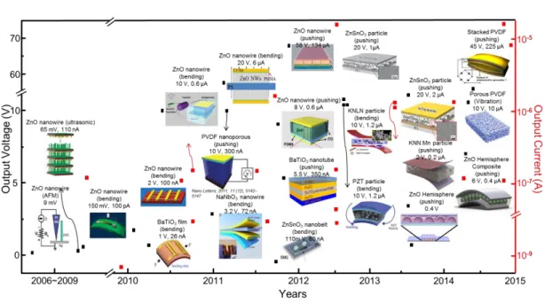
Energy harvesting technologies may meet critical demand in areas where alternatives to fossil fuels are required for environmental protection, and in portable applications that require super-high energy capacity or complementary energy sources. Harvesting energy from ambient energy sources including solar [1–8], thermal [9], and mechanical energy [10-18], has attracted intensive interest in the past years to meet these needs. Among these, piezoelectric and triboelectric harvesting technology [12,14,19,20], which converts mechanical energy, the most common energy source available anywhere at any time, into electrical energy, has been proposed and investigated by many researchers because of an extended life time, no recharging procedures, and scalability. To date, there have been attempts to fabricate piezoelectric energy harvesting devices, named as nanogenerators, by employing various piezoelectric nanostructures including nanowires [14, 21–24], nanotubes [25], and porous structures [26], in which most works have been focused on nanowire-type generators. However, these technologies still suffer from many drawbacks that limit the successful commercialization.
Recently, thin film-type nanogenerators with perovskite ceramic materials (BaTiO3 and ZnSnO3) [27, 28] were also demonstrated, generating a much higher level of power density than other similar structural or related devices. The advent of nanogenerator and nanotechnology may significantly lead to a self-powered system, based on driving portable devices with low power consumption by harvesting energy from ambient energy sources.
Recent development in sensor technologies has provided innovative ways to reduce power consumption up to less than 1 mW [29, 30], enough to be produced by nanogenerators.
Nanogenerator-assisted self-powered magnetic [31], chemical [32], temperature [33], and mechanical sensors [34] have been successfully demonstrated. This approach can greatly enhance the adaptability, mobility, and durability of such sensors.
Figure 1. The process of output voltage and current of piezoelectric nanogenerators.
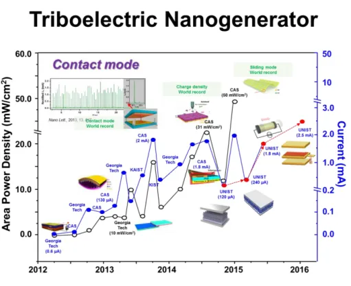
Figure 2. The process of output power density and current of triboelectric nanogenerators.
In addition, the triboelectric effect has been utilized as an effective way to harvest mechanical energy. Contact between two materials with different triboelectric polarity yields surface charge transfer. The periodic contact and separation of the oppositely charged surfaces can create a dipole layer and a potential drop, which drives the flow of electrons through an external load in responding to the mechanical stimulation. As for TENG, maximizing the charge generation on opposite sides can be achieved by selecting the materials with the largest difference in the ability to attract electrons and changing the surface. For the plate-structured TENG, it needs more time and stronger applied force to ensure the contact and separation of the two oppositely charged material surfaces upon pressing and releasing are complete, especially under the electrostatic attraction between them. Adding spacers between two plates or using arch-shaped substrates have been demonstrated to improve the output of TENG [35].
Currently, various kinds of nanoparticles or nanowires are used to decorate the triboelectric materials, for increasing the friction between two contact materials in the TENG. However, due to the soft and ductile behavior of nanoparticle/nanowires, the performance of the TENG is generally degraded under large applied force, and therefore power stability is strongly demandable.
Although contact electrification, also named as triboelectrification, is one of the oldest and most universally-existing phenomena in the nature and people’s daily life, the understanding of its fundamental mechanisms is rather poor and the proposed mechanisms remain highly debated, so that we do not know how to effectively control the density of the triboelectric surface charges through material or surface modification to enhance the output power. Both the voltage and the current outputs of the TENGs are proportional to the triboelectric charge density on the surface [36, 37], so that the output power has a quadratic dependence on the charge density. Therefore, a key approach for the improvement of TENG’s output performance from the materials aspect is to increase the triboelectric charge density through material optimization and surface functionalization. Furthermore, modification of work function and electron affinity between two
materials are required to effective charge and electron transfer.
Thus, I will study flexibility and stability-dependent output performance for piezoelectric nanogenerators based on porous platforms, and capacitance variation and work function control of triboelectric surfaces for TENG. Additionally, several types of nanostructures for very flexible, stable, and high output performance of the nanogenerators which are mainly based on the porous nanostructured platforms. For example, pressure sensors and piezoelectric nanogenerators based on embossed hollow hemispheres thin films and the asymmetric hemispheres with using oblique angle sputtering to show high sensitive output current signal and demonstrate enhanced output voltage by a layer-by layer stacking. The flexible and stretchable composites embedded by piezoelectric hemispheres are investigated according to the bending direction for health monitoring. Further, the output performance of a rationally designed TENG by utilizing the contact electrification between a porous film and a metal foil will be shown according to capacitance variation under external force. To remove unnecessary specific spacer, a new type of TENG structure, in which the key layer consists of a sponge-like structure and Au nanoparticles embedded in pores, is introduced. Additionally, the mesoporous film become more flexible, increasing the contact area in sponge film when the external forces were applied. PDMS and Au nanoparticles have the different triboelectric tendency and make large triboelectric charges in each pore upon contact, which can add up with generated charges in the whole device, leading to enhanced surface charge density and thus higher electrical output performance.
CHAPTER 2. THEORETICAL BACKGROUND AND MOTIVATION
2.1 Piezoelectricity
2.1.1 Introduction to piezoelectricity
Piezoelectricity was first discovered in 1880 by Pierre and Jacques Curie when they found that certain crystals, most notably quartz and Rochelle salt, produced a surface charge under a compressive load. This generation of electric charge under mechanical loading is known as “direct piezoelectric effect”. One year later, the opposite (or converse) piezoelectric effect, where an induced voltage could cause mechanical deformation, was mathematically proven by Gabriel Lippman and later experimentally observed by the Curie brothers. The natural crystals that were initially discovered exhibited weak coupling between the mechanical and electrical domains. More recently however, synthetic piezoelectric materials have been created with increased coupling that enable the use of piezoelectricity in practical applications.
The piezoelectric effect exists in several crystalline materials due to the polarity of the unit cells within the material. This polarity leads to the production of electric dipoles in the material which give rise to the piezoelectric properties. The application of mechanical strain causes rotation of the dipoles, leading to an apparent charge flow that can be measured as current by placing electrodes on opposite faces of a piezoelectric material (direct piezoelectric effect).
Similarly, the application of a voltage across the material will cause rotation of the dipoles which results in an induced strain in the material (converse piezoelectric effect). Both the direct and converse piezoelectric effects can be described mathematically through the piezoelectric constitutive equations, given in their most common form as
{𝑆 𝐷 } = [𝑠
𝐸𝑑′
𝑑 𝜀
𝑇] {𝑇 𝐸 }
where S is the mechanical strain, D is the electric displacement, T is the mechanical stress, E is the electric field, sE is the mechanical compliance (reciprocal of the elastic modulus) measured at constant electric field (denoted by the superscript E), d is the piezoelectric strain constant, and εT is the dielectric permittivity measured at zero mechanical stress (denoted by the superscript T).
The electromechanical coupling of piezoelectric materials allows their ability to act as both sensors when operating in the direct effect, and as actuators when operating in the converse effect, thus piezoelectric material is a versatile solution in many applications. A wide variety of piezoelectric devices are available commercially. The most common piezoelectric material is lead zirconate titanate, a piezoelectric ceramic known as PZT. Piezoelectric ceramics are widely used, however, they are extremely brittle. In an effort to create flexible piezoelectric material, several piezoelectric fiber-based materials have been developed. These materials contain thin extruded strands of piezoceramic fiber embedded in an epoxy matrix with flexible surface electrodes. Piezoelectric fiber-based materials have the advantage of being flexible and can be mounted on curved surfaces, however, their coupling is typically weaker than that of monolithic ceramics. Additionally, piezoelectric polymer material, most notably polyvinylidene fluoride or PVDF, provides the highest degree of compliance but the weakest coupling. The wide range of piezoelectric materials allows for their use in a variety of diverse applications.
2.1.3 Piezoelectric energy harvesting
Energy harvesting technology is one of means of converting ambient mechanical energy into electrical energy, which is typically used to power and generate the electronic devices. Piezoelectric based energy harvesting includes the placement of a piezoelectric device
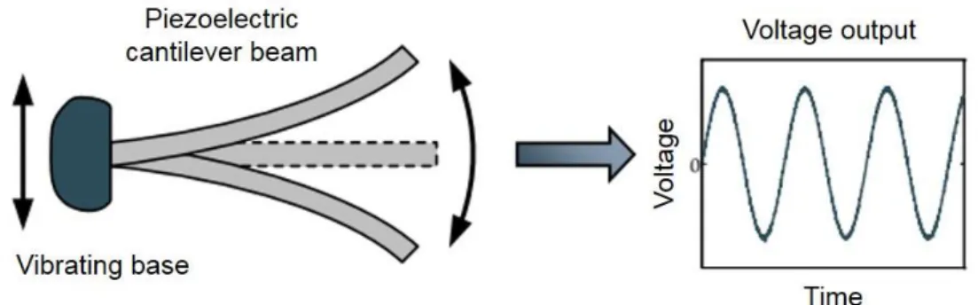
under surrounding vibration to utilize the electromechanical coupling for piezoelectric materials to generate the electrical energy. The conventional piezoelectric based nanogenerator is the cantilever structure as shown in Figure 3. Optimized output performance of the cantilever-structured nanogenerator is obtained under the spectific frequency of surrounding vibration matched to the resonant frequency of the cantilever beam. Under vibration condition, maximum vibration energy could be converted to the nanogenerator and to useful electrical energy to us. In general, deviations from resonance cause significant decreases in output performance, therefore, tuning and optimizing the nanogenerator is critically required. Many researches have shown to investigate alternative charactersitcis for piezoelectric nanogenerators, such as nonlinear configurations using magnetoelastic nonlinearity [38–40], in an effort to create broadband nanogenerator structures.
Figure 3. Schematic image of cantilever-structured piezoelectric nanogenerator and its output voltage generation.
In general, the electrical energy generated by piezoelectric nanogenerators is in the form of high output voltage, low current alternating current (AC) signals, where the portable and wearable electronic devices to be powered require low voltage direct current (DC) power supplies. Piezoelectric nanogenerator is usually used in powering small electronics such as sensor nodes. Therefore, suitable circuit for piezoelectric nanogenerator must be used to
condition the piezoelectric output to a usable form. Basic conditioning circuitry typically contains a rectifier unit and smoothing capacitor to perform AC to DC conversion as well as a simple storage medium. Typically, the instantaneous energy generated by a piezoelectric nanogenerator is inadequate for powering electronics, therefore, a storage medium (such as a Li-ion secondary battery or capacitor) is often used to temporarily store the harvested energy.
In this case, an operational duty cycle can be defined in which the frequency of operation of the device to be powered is described based on the amount of generated power and the power required to operate the electronic device. The power output of a piezoelectric nanogenerator depends significantly on the impedance of the circuit or load connected to the piezoelectric nanogenerator. A matched load exists for each piezoelectric device as well as for each excitation frequency. Several researchers have investigated the design of optimized circuits to improve the energy conversion efficiency. [41-43] Recently, the development of impedance matching circuitry in which the circuit and storage medium appear as a pure matched external load for maximum power transfer has been investigated as well. [44] The topic of piezoelectric energy nanogenerator has attracted much attention throughout the research community in the past decade. Several aspects of piezoelectric energy nanogenerator have been investigated including the development of novel piezoelectric materials, mechanical structures to optimize power output, electronic control and harvesting circuitry, and mathematical models used to predict the response of piezoelectric systems. Several review articles have been published highlighting the major work in the field. [45-48]
2.2 Triboelectricity
When two different materials are brought into contact and separated, an electric charge is transferred from one to the other. This phenomenon is often called ‘contact charging’ or
‘contact electrification’,in which certain materials become electrically charged after they come into frictive contact with a different material. Rubbing glass with fur, or a comb through the hair, can build up triboelectricity. When they are rubbed against each other, it can be called
‘frictional electrification’, ‘triboelectric charging’, or simply ‘tribo-charging’; as for short contact during collision, it can be called ‘impact charging’. In practice, it is not easy to classify the contacting process for charge transfer purposes into groups, such as sliding, rolling, and impact, and thus the term ‘triboelectric charging’ is used in such abroad sense.
2.2.1 Mechanism for contact charging and charge transfer
I start with the well-established concept of electron transfer based on the contact potential difference (CPD) due to a difference of work functions for metal-to-metal contact.
The triboelectric charging of metals is usually unnoticeable since the charge transferred moves away from the contact point due to its conductivity. However, when the metals are isolated electrically after the contact, the transferred charge can be measured. The charge transfer is explained in terms of ‘electron transfer’ arising from the difference in work function between the surfaces. Two metals with different work functions ϕ1 and ϕ2 in contact are schematically shown in Figure 4. Assuming that electron transfer takes place by tunneling so that thermodynamic equilibrium prevails, the contact potential difference Vc is given by
𝑉𝑐 = 𝑉1/2 = −(∅1− ∅2) 𝑒
where V1/2 is the contact potential difference of metal 1 against metal 2, e is the elementary charge [49]. The amount of the transferred charge is equal to the product of the contact potential difference and the capacitance between the two bodies. The capacitance depends on the state of the contacting surfaces. Although the position of the electrons can vary after the metals are separated, the net charge transferred Δqc is approximated by the following equation:
∆𝑞𝑐 = 𝐶0𝑉𝑐
where C0 is the capacitance between the bodies at the critical separation distance where the charge transfer is cutoff. The difference is probably caused by uncertain factors, such as surface roughness, impurities, oxidized layer, separation speed, and others.
Figure 4. Electron potential energy for metal–metal contact.
2.2.2 Triboelectric energy harvesting
Traditional TENG is a mechanical device that produces static electricity or electricity at high voltage by contact charging. The most popular ones are the Wimshurst machine and Van de Graaff generator, which were invented in ~1880 and 1929, respectively. Both machines use the accumulated static charges generated by triboelectrification; the tribo-charges are transferred from a rotating belt to a metal brush by the corona discharging (e.g., the electric- field-induced arching of air); once the accumulated charge density reaches a critical value,
discharging over two opposite electrodes occurs. It appears that the traditional TENG is a high voltage source, and there is no current unless there is a discharging.
However, in early 2012, this phenomenon systematically studied and found that it was a triboelectrification-driven energy conversion process. [50] This was the birth of the TENG, which is distinctly different from the traditional Van de Graaff generator in a way that electrostatic induction is introduced for output power. The operating principle of the TENG for the case of dielectric-to-dielectric in contact mode can be described by the coupling of contact charging and electrostatic induction. [51]
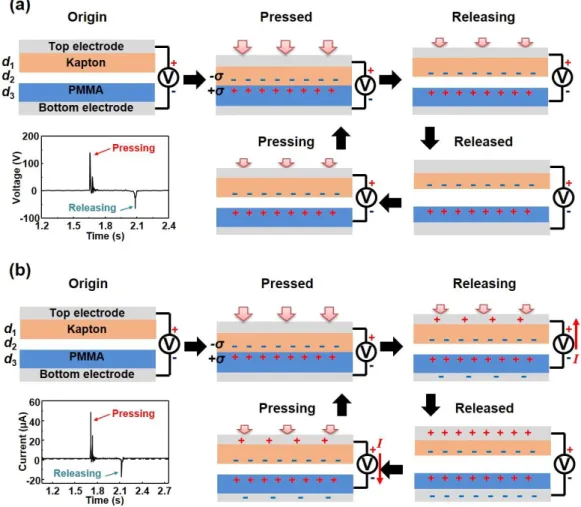
Figure 5. Schematic diagrams that illustrate the operating principle of the generator. (a) Open-circuit condition. (b) Short-circuit condition.
Respectively, Figures 5a and 5b depict electric output of open-circuit voltage and short- circuit current. In the original state, no charge is generated or induced, with no electric potential difference (EPD) between the two electrodes. With an externally applied force, the two polymers are brought into contact with each other. Surface charge transfer then takes place at the contact area due to triboelectrification. According to the triboelectric series [52,53], which is a list of materials based on their tendency to gain or lose charges, electrons are injected from PMMA into Kapton, resulting in net negative charges at the Kapton surface and net positive charges at the PMMA surface, respectively. It is worth noting that the insulating property of the polymers allows a long-time retention of triboelectric charges for hours or even days. Since they are only confined on the surface, charges with opposite signs coincide at almost the same plane, generating practically no EPD between the two electrodes.
As the generator starts to be released, the Kapton film tends to revert back to its original position due to its own resilience. Once the two polymers separate, an EPD is then established between the two electrodes. If we define electric potential of the bottom electrode (UBE) to be zero, electric potential of the top electrode (UTE) can be calculated by
𝑈𝑇𝐸 = −𝜎𝑑′
𝜀0
where σ is the triboelectric charge density, ε0 is the vacuum permittivity, and d0 is the interlayer distance at a given state. As the generator is being released, Voc increases until reaching the maximum value when the Kapton film fully reverts to the original position. Such a signal will remain constant provided that the input impedance of the electrometer is infinitely large. If pressing is immediately followed, the EPD starts diminishing as the two polymer layers get closer to each other. As a result, Voc drops from the maximum value to zero when a full contact is made again between the two polymers. If the two electrodes are shorted, any established EPD shown in the above equation as the two polymers separate drives electrons to flow from
the top electrode (TE) to the bottom electrode in order to balance the generated triboelectric potential, resulting in an instantaneous positive current during the releasing process. The net effect is that induced charges accumulate with positive sign on the top electrode and negative sign on the bottom electrode. The induced charge density (σ0) when the generator is fully released is given by [51]
𝜎′= 𝜎𝑑′𝜀𝑟𝑘𝜀𝑟𝑝
𝑑1𝜀𝑟𝑝+ 𝑑′𝜀𝑟𝑘𝜀𝑟𝑝+ 𝑑2𝜀𝑟𝑘
where εrk and εrp are the relative permittivity of Kapton and PMMA, respectively, and d1 and d2 are the thicknesses of the Kapton film and the PMMA layer. The maximum value of σ’max
is obtained by substituting d3 for d0 in the equation above. Once the generator is pressed again, reduction of the interlayer distance would make the top electrode possess a higher electric potential than the bottom electrode. As a consequence, electrons are driven from the bottom electrode back to the top electrode, reducing the amount of induced charges. This process corresponds to an instantaneous negative current. When the two polymers are in contact again, all induced charges are neutralized.
CHAPTER 3. OBJECTIVE AND IDEAS 3.1 Flexibility for stable output performance
In terms of the nanogenerators, a high flexibility or stretchability is essential in generating high-power continuous electric output signals. The high flexibility can provide an opportunity applicable to a target object without any limitation of its shape and movement.
Several research efforts have demonstrated the realization of nanogenerators with high flexibility in which the polymer-mold-supporting nanogenerators [54] fabricated using various nanostructured piezoelectric materials like ZnO [54], BaTiO3 [55], KNbO3 [56], ZnSnO3 [57], and NaNbO3 [58] have been considered as one of promising platforms for the large-scale and super-flexible nanogenerators. However, they are still difficult to be utilized as an efficient approach for super-flexible nanogenerators owing to the high-cost and the low-throughput process. Actually, the most composite-type nanogenerators have been based on the nanowires [58] and nanoparticles. [57, 58] For the nanowires, the synthesis methods are available only for a limited number of piezoelectric materials such as ZnO and GaN. Furthermore, it also takes a long time (~ several hours) to synthesis such nanowires by a hydrothermal method, a well- known process for the growth. [55-59] The power generation of nanoparticles-embedded nanogenerators is critically dependent on the mode of the applied force and it is likely to be mostly feasible only under large pushing force and/or after an electrical poling treatment. [55]
Thus, it is necessary to develop innovative strategies applicable to any target objects regardless of the mode and magnitude of the applied force.
3.2 Difference in work function between two materials for electron transfer
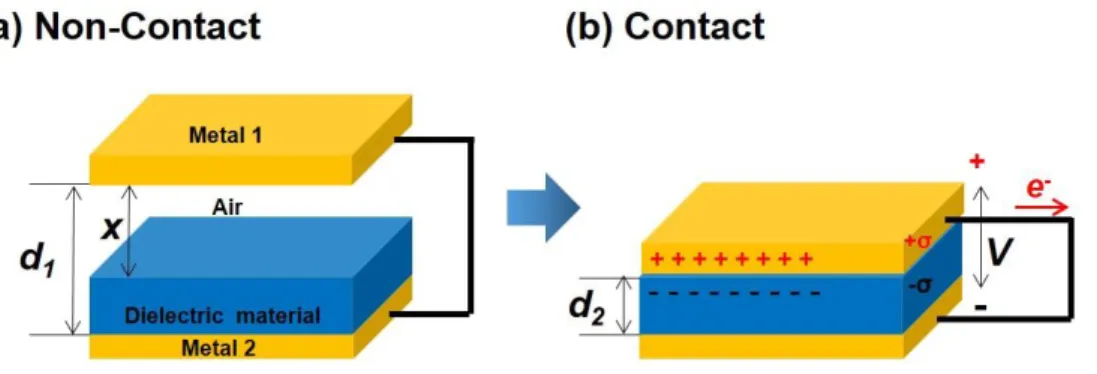
Most recently, a new type of power generating device, named as TENG based on triboelectric effects coupled with electrostatic effects have been demonstrated as powerful means of harvesting mechanical energy from living environment. In traditional TENGs, the two materials were chosen according to the difference in surface potentials, e.g., the polymer material (i.e. Teflon) terminated with the most electronegative functional group as the negative side and the low work function material (i.e. Al metal) as the positive side, apart from each other (named as airgap). When the two materials are contacted, the polymer material at the negative side tends to gain electrons from Al metal, resulting in being negative compared with Al. (Figure 6)
Figure 6. Theoretical models for vertical contact-mode triboelectric nanogenerator (a) before contacting and (b) after contacting.
Thus, a key approach to improve the electrical output performance of the TENGs from the materials aspect is to increase the triboelectric surface charge density through material modification and surface functionalization. In this study, the material modifications of the surface potential in TENGs have focused. Additionally, the increased density of surface charges primary determined by the intrinsic properties of the specific materials and the effective means to
enhance the output power of TENGs have proposed, which are critically important for improving the output performance of TENGs.
Figure 7. Energy band diagrams for the metal and dielectric materials in separation equilibrium (a) before contact, (b) contact, (c) after contact, and (d) work function control.
The enhancement of the electrical output performance may be attributed to the relative change in the surface potential level of the dielectric layer and the bottom electrode. As mentioned above, a potential difference is produced between the metal and dielectric by the contact due to different triboelectric tendency. Thus, the potential difference with the Fermi level of the bottom electrode will increase output performance of TENGs. The transferred charge density (σ) on the PDMS surface is defined as
𝜎 =
[(𝑊−𝐸0)/𝑒](1+𝑡/𝜀𝑧)𝑡/𝜀𝜀0+(1/𝑁̅̅̅̅̅̅̅̅𝑒𝑠(𝐸) 2)(1+𝑡/𝜀𝑧)
where W-E0 is the difference in the effective work functions between two materials, e, t, ε, ε0,
z, and 𝑁̅̅̅̅̅̅̅̅𝑠(𝐸) are the charge of an electron, distance of space, relative permittivity of dielectric layer, vacuum permittivity of free space, depth of mesoporous film, and the averaged surface density of states [60, 61]. (Figure 7) Additionally, I calculated transferred charge density output voltage of TENGs with various work functin difference, resulting in the increase of output performance of TENGs. Thus,the probability of the charge transfer and the surface charge density will increase due to the control of difference in work function between two materials. (Figure 8)
Figure 8. (a) The calculated charge density and (b) output voltage under work function control between the metal and dielectric material in separation equilibrium.
3.3 Dielectric constant of insulating layer for high surface charge density
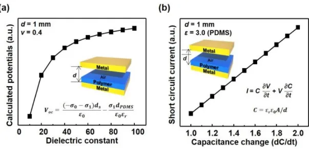
Moreover, if PDMS is mixed with a co-mixture of ZnO and carbon nanotubes [62] or BaTiO3 and graphite carbon [63], the generator achieves a higher output power. Because it is that the dielectric constant of the PDMS layer is very important for a TENG with a capacitor structure, as well as the role of the carbon nanostructures in the polymer. Additionally, I calculated triboelectric potential distributions of TENGs with various dielectric constants by using COMSOL multi-physics package, resulting in the increase of output performance of TENGs. Thus, the outputs and the surface charge density will increase due to the dielectric constant of insulating layer. (Figure 9) Recently, sponge-structured PVDF- and PDMS-based TENGs have been found to possess better output power, compared with the flat film-based TENG. [64, 65]
Figure 9. (a) Theoretical model for the vertical contact-mode TENG and (b) COMSOL multiphysics simulations of the electric potential distributions for TENG with dielectric
constant (ε) of 10 and 100.
The reports proposed that a sponge-structured film are thinner than a flat film, which increases the relative capacitance by the increase in the effective (ε/d) value. To determine how the effective ε/d value affects the output power of TENGs and whether there is a relationship between the effective ε/d value and mixture of nanomaterials, we assume that it is necessary to investigate the role of high dielectric nanomaterials mixed into insulating layer (polymer) in TENG for large surface charge density. Thus, I calculate the potential difference and short circuit current with increase of dielectric constant (ε) and capacitance change (dC/dt) per unit time of polymer in TENG. It is clearly seen that increase of the calculated potential difference and short circuit current due to the dielectric constant and capacitance change per unit time in polymer of TENGs. (Figure 10)
Figure 10. (a) The calculated potentials and (b) short circuit current with increase of dielectric constant and capacitance change of polymer in TENG.
CHAPTER 4. EXPERIMENTAL PROCEDURE 4.1 Embossed hollow hemispheres thin films
4.1.1 Highly responsive Pressure Sensor
An aqueous suspension of 1-μm-diameter polystyrene beads (2.6 wt%, Polysciences, Warrington, USA) was used to prepare close-packed monolayer bead templates for the fabrication of embossed ZnO films, as described previously. Briefly, prior to spin-coating of the suspension on bare SiO2/Si (for pressure sensors) and ITO-coated SiO2/Si (for nanogenerators) substrates, the bare substrate was treated with UV/Ozone (AHTECH LTS, South Korea), making the surface of the substrate hydrophilic. A drop of polystyrene bead suspension was then pipette onto the SiO2/Si substrate. Spin-coating of the polystyrene beads was done at 1300 rpm for 3 s, and then the sample was dried for 1h in a dry box at room temperature. The spinning speed and slow drying were optimized because both were critical in obtaining monolayer bead templates without sphere-free regions or agglomeration. A 200-nm- thick ZnO film was deposited onto the substrates at room temperature by a RF sputtering, and it can be optimized further for a better device performance. The base pressure, working pressure, rf power, and gas flow rate were 1×10⁻⁶ Torr, 4mTorr, 16/4 sccm (Ar/O2), respectively.
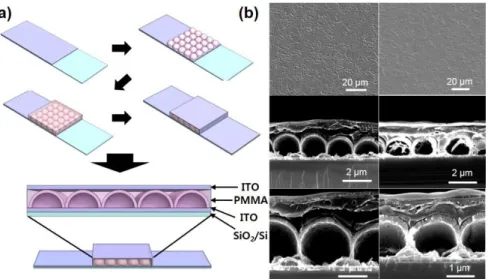
The hemispheres with asymmetric shapes were formed by OAD using a RF sputtering with a vapor flux angle of 85o. The samples were calcined in air at 300oC for 60 min to burn out the polymer beads and simultaneously crystallize the ZnO film, resulting in an embossed ZnO film with hollow hemispheres on the substrate. (Figure 11)
4.1.2 Piezoelectric nanogenerator
For nanogenerators, a layer of 2 μm thick poly(methyl methacrylate) (PMMA) was spin-coated on the embossed ZnO films. As a top electrode, ITO layer was then placed above the heads of the embossed ZnO films. A nanogenerator was also made by stacking two pieces of the hemispheres. (Figure 12)
Figure 11. (a) Schematic diagrams of the pressure sensor fabrication process. (b) Hexagonally close-packed 2D arrays as a form of multi-domains of areas larger than approximately 20 μm2. Oblique angle deposition of ZnO ( = 85o) produced asymmetric
hemispheres.
Figure 12. (a) The schematic diagrams of the nanogenerator fabrication process. (b) Low and high magnification SEM images of the nanogenerator.
4.2 Piezoelectric hemispheres with stretchable composite films
An aqueous suspension of 0.5, 1, 3, and 10-μm-diameter polystyrene (PS) beads (2.6 wt%, Polysciences, Warrington, USA) was used to prepare close-packed monolayer beads template for the fabrication of crescent shape periodic structures embedded in the polydimethylsiloxane (PDMS) layer. The SiO2/Si substrate was treated with UV/Ozone (AHTECH LTS, South Korea) to make the surface of the substrate hydrophilic. Langmuir–
Blodgett deposition of the PS beads was done for single layer films, and then the samples were dried for 24 hrs in a dry box at room temperature. I found that the slow drying process was essential in obtaining monolayer beads template without sphere-free regions or agglomeration.
A 100 nm-thick ZnO film was deposited on the PS spheres at room temperature by a RF sputtering. The base pressure, working pressure, rf power, and gas flow rate were 1×10⁻⁶ Torr, 4 mTorr, 16/4 sccm (Ar/O2), respectively. A 100 nm-thick piezoelectric lead zirconate titanate
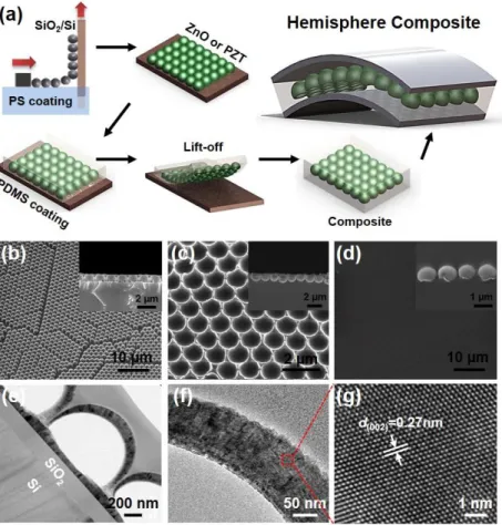
(PZT) film was also deposited at room temperature by the RF sputtering, in which the deposition power, base pressure, working pressure, and Ar flow rate were maintained at 80 W, 2 × 10⁻⁶ Torr, 3 mTorr, and 30 sccm, respectively. The samples were calcined in air at 300 oC for 60 min to burn out the polymer beads and simultaneously crystallize the films, resulting in embossed films with hollow hemispheres on the substrate. The PZT film was then additionally annealed at 650 oC for 5 min in O2 ambient (10 Torr) to enhance the crystallization of the materials. The PDMS solution was poured into the PS sphere template and allowed to solidify into an amorphous free-standing film by heating on a hotplate at 90 oC. The PDMS film was then detached from the substrate and soaked in acetone for 24 h to remove the PS spheres, producing free-standing PDMS film with crescent-shape structures. To fabricate composite- type devices, the crescent shape structures were filled by another PDMS layer without any voids between the piezoelectric materials and PDMS. ITO/PET films are then attached on the top and bottom sides of the structures, which act as the top and bottom electrodes. A nanogenerator was also made by stacking two pieces of the structures. (Figure 13)
Figure 13. (a) Schematic diagrams of the fabrication process for the piezoelectric hemispheres embedded stretchable composites. SEM images of (b) hexagonally close-packed
2D ZnO hollow hemisphere arrays as a form of multi-domains of areas larger than approximately > 10 cm2, (c) detached hemisphere array from the substrate, and (d) piezoelectric hemispheres embedded composites. (e) A cross-sectional TEM image results of
ZnO hemispheres, which reveal that the hemispheres are hollow. (f) The HR-TEM images also show that the hemisphere has columnar structures with grain sizes in the range of 10 – 20 nm. (g) High crystallinity of each grain, based on facts that the most part of the grains is
bright in dark field image and lattice fringes are well ordered.
4.3 Highly ordered sponge structured films
In the experiment, first, an aqueous suspension of PS spheres (2.6 wt%, Polysciences, Warrington) was used to fabricate the PDMS inverse opal structured film. Many layers of PS spheres with diameters of 0.5, 1, 3, and 10 µm were stacked in a face-centered cubic structures mode onto a SiO2/Si substrate in order to synthesize different diameters/pore size of sponge structured film, and for their respective sponge-structured TENGs fabrication. Then, PDMS solution was poured in to the periodically arranged PS spheres, and allowed to solidify into an amorphous free-standing film by heating on a hotplate at 90 oC. Further, to obtain the PDMS inverse opal structured film, the PDMS matrix was detached from the substrate, and soaked in acetone for 24 h in order to remove the PS spheres. The effective area and thickness of both flat and sponge-structure film were 1 cm x 1 cm and 300 µm, respectively. The spacer was made of an insulating polymer film with double-sided adhesive with a thickness of 0.03 mm.
(Figure 14)
Figure 14. (a) Structure and fabrication process of the sponge structure-based TENG. (b) FE- SEM images of the sponge structure-based TENG.
4.4 Mesoporous Pores Impregnated with Au Nanoparticles
Polydimethylsiloxane (PDMS) (Sylgard 184, Dow Corning) was used as the polymer layer with many pores, which was prepared by the gel-casting technique. The solution of mixed base monomer and curing agent in a mass ratio of 10 : 1 was dropped on the beaker. The air remaining in the PDMS was removed by a vacuum process, and PDMS mixed with deionized (DI) water. The mass ratio between DI water to PDMS was adjusted to create different porosity.
The mixture was stirred for 30 min and yielded a uniformly-mixed PDMS/DI water suspension.
The suspension was cast into a film shape in a blocking layer on SiO2/Si substrate and dried in atmosphere at 90 °C to remove the DI water and create air voids in PDMS. After The PDMS film layer was peeled off from the substrate, mesoporous structured PDMS film was obtained.
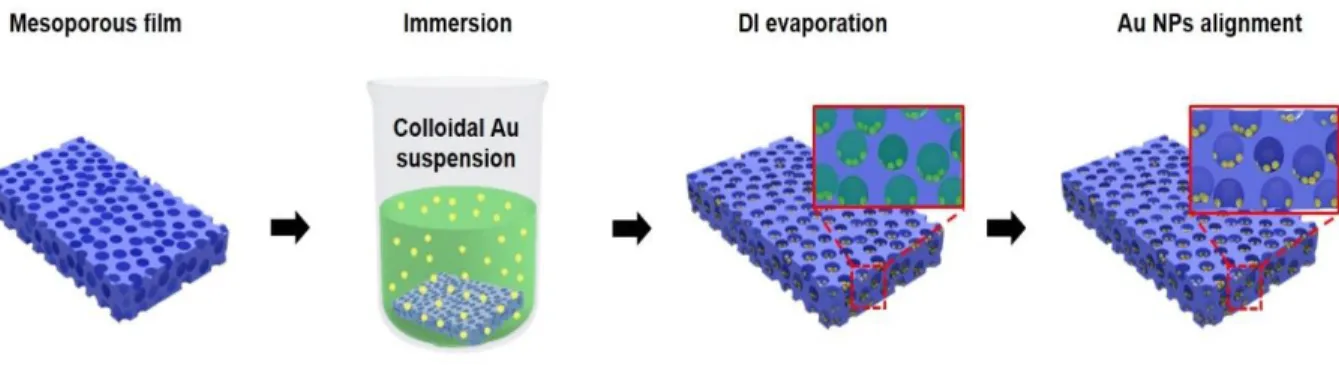
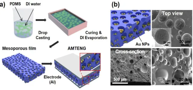
To position Au NPs on the bottom side of pores in mesoporous film, the mesoporous film was dipped into the 100 nm colloidal Au suspension (BBI International, UK) for 5 hrs and was taken out. After cleaning the surface of the film with DI water, the mesoporous film with Au NPs and DI water was then dried slowly in atmosphere at room temperature for 72 hrs to remove DI water. This slow drying process is very important to get the nanoparticles to be located on the bottom sides of the pore (Figure 15). To fabricate nanogenerator, the 10 μm- thick PDMS film was produced on the Al electrode attached by the double sided polyimide tape, as shown in the schematic fabrication process of the TENGs (Figure 16a). The mesoporous PDMS film was then attached on the layer and was covered with same PDMS film/polyimide/Al electrode, followed by the drying process in atmosphere at 90°C for 1 hr. In the cross sectional optical and SEM images, it was found that there was no gap between these layers (Figure 16b). Finally, the fabricated Au nanoparticles-embedded mesoporous TENG is shown in Figure 17.
Figure 15. The schematic fabrication process of the Au NPs embedded mesoporous films.
Figure 16. (a) Schematic diagrams of the fabrication process for the top and bottom electrode of the Au nanoparticles-embedded mosoporous TENG without airgap. Cross-sectional optical and SEM images of the Au nanoparticles-embedded mosoporous TENG without airgap (b)
before and (c) after the generator operates for 1000 cycles.
Figure 17. (a) Schematic diagrams of the fabrication process for the Au nanoparticles- embedded mosoporous TENG. (b) Top and cross-sectional SEM images of mesoporous PDMS film with Au NPs (0.28 wt%). The insets show the morphology of Au NPs and cross-
sectional SEM images of mesoporous film.
4.5 Measurement of electrical characteristics
The output voltage and current density of the embossed thin film generators are measured under pushing and bending condition, which are detected by a Keithley 6485 picoammeter, Keithley 2182A nanovoltmeter of 10 GΩ resistances, Tektronix DPO 3052 Digital Phosphor Oscilloscope, and a low-noise current preamplifier (model no. SR570, Stanford Research Systems, Inc.). A pushing tester (Labworks Inc., model no. ET-126-4) was used to create vertical compressive strain in the nanogenerator. Nanoindentation tests were carried out at a constant indentation strain rate of 0.05 s-1, with a maximum indentation depth of 20 µm with Berkovich indenter, using the DCM II module in Nanoindenter G200 made by Agilent Corporation. Capacitance in force-response curve were calculated using equation
C=ε0εrA/d, where ε0, εr, A, and d are the permittivity of free space (8.854×10⁻¹² Fm-1), relative static permittivity (1.0 - 3.0), contact area (1 cm2), and distance (300 µm) between top and bottom electrodes, respectively.
4.6 Microstructural analysis
The morphologies of embossed hollow hemisphere thin films were characterized by a Nano 230 field emission scanning electron microscope (FEI, USA). Transmission electron microscopy was performed using a transmission electron microscope (JEOL, Japan). A dual- beam focus ion beam (FEI, USA) was used to prepare the TEM samples. The crystalline properties of the films were characterized by a high resolution X-ray diffractometer (Bruker, Germany). For in-situ tension test, a force applied when the films was stretched was measured by using the tensile tester (AGS-100N, Shimadzu, Japan) under conditions of a speed of 5 mm/min at a distance of 5 mm.
CHAPTER 5. RESULTS AND DISCUSSION
5.1 Highly responsive pressure sensor based on embossed hollow hemisphere 5.1.1 Crystal characteristics
The schematic diagrams of the pressure sensor fabrication process are shown in Figure 11a and detailed information described in Experimental section. Scanning electron microscopy (SEM) images in Figure 11b shows that the 2D ZnO hollow hemisphere arrays are hexagonally close-packed as a form of multi-domains of areas larger than approximately 20 μm2. By a spin coating method of PS spheres, quasi-continuous 2D array monolayers which fill the entire substrate of > 10 cm2 area are studied in the current study. By heating at 300 oC for 1 h in air, it produces ZnO embossed thin films with hemispheres, well-distributed on the substrates.
The microstructure and crystalline properties of the embossed ZnO thin films were characterized by transmission electron microscopy (TEM) and X-ray diffraction (XRD). In the XRD spectrum (Figure 18a), there is only one peak corresponding to the (0002) plane of ZnO, showing preferred orientation of ZnO thin films. As the angle between substrate normal and vapor flux increases, the peak shifts to the higher angle by 0.3o and the Full-Width-Half- Maximum (FWHM) decreases from 0.32o to 0.3o, meaning an improvement in the crystallinity of the embossed films deposited by OAD. Figure 18b shows a cross-sectional TEM image of asymmetric hemispheres, which reveals that the hemispheres are hollow. Clearly, a film was deposited directly on the substrate although the bottoms of the hemispheres fold into the hollow inner space. The elemental maps, determined by energy dispersive X-ray (EDX), of an embossed ZnO thin film confirms the formation of asymmetric hemispheres consisting of Zn and O atoms. The high-resolution TEM (HR-TEM) images show that the film clearly reveals
columnar structures with grain sizes in the range of 10 – 20 nm. Each grain seems to be highly crystalline, based on the facts that the most part of the domains is bright in dark field image, lattice fringes are well ordered. Furthermore, high magnification at the domain interface clearly shows the crystalline continuity between the grains, indicating that the embossed ZnO films enable reliable device action. It can also be seen that there are some stacking faults at the interface since the grains are fan-shaped (it means that the grain size increases from bottom to top).
Figure 18. (a) The XRD patterns of ZnO thin films with symmetric and asymmetric hollow hemispheres on SiO2/Si substrate. (b) A cross-sectional TEM image and EDX results
of asymmetric shaped hemispheres, which reveals that the hemispheres are hollow and consist of Zn and O atoms. The HR-TEM images also show that the hemisphere has columnar structures with grain sizes in the range of 10 – 20 nm. High crystallinity of each grain, based on facts that the most part of the grains is bright in dark field image and lattice
fringes are well ordered.
5.1.2 Output performance
Figure 19a shows the change of the current density with the applied voltage of 10 mV when the external force of 30 N is applied. For thin film and embossed thin film with symmetric hemispheres, there is no change in the current density when I push the samples, as shown in the inset, although there is a little change (< 0.05 mA/cm2) in the embossed film by the force.
By making the hemispheres asymmetric, a sharp current pulse up to 7 mA/cm2 was clearly observed when the sample was pushed quickly. The unsymmetrical pressure between the tensile and compressive stressed region in hemispheres along lateral direction causes a gradient in the piezoelectric potential, resulting in the control of the current direction and level to be approximately 7 mA/cm2 at the normal force of 30 N. The sensitivity of asymmetric hemisphere is 2.3 pA/Pa. The change of current density by a pushing force in embossed films with hollow hemispheres can be understood from the piezoelectric potential distributions inside a hemisphere along the direction (Figure 19b).
Figure 19. (a) The change of the current density with the applied voltage of 10 mV when the external force of 30 N is applied and (b) piezoelectric potential distributions inside a
hemisphere along the direction (transverse and vertical) for symmetric (top) and asymmetric (bottom) hollow hemispheres.