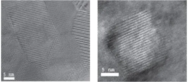
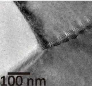
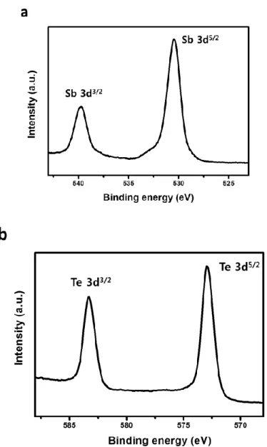
XPS spectra of Sb2Te3 ChaM dried at room temperature near (a) Sb region and (b) Te region. SEM images of the annealed n-type materials (a) with and (b) without ChaM, and p-type materials (c) with and (d) without ChaM. SEM images of the dried samples of (a) n-type and (c) p-type and EDS mapping of (c) n-type and (d) p-type samples.
Introduction
Back ground of thermoelectric phenomenon
- The Seebeck effect
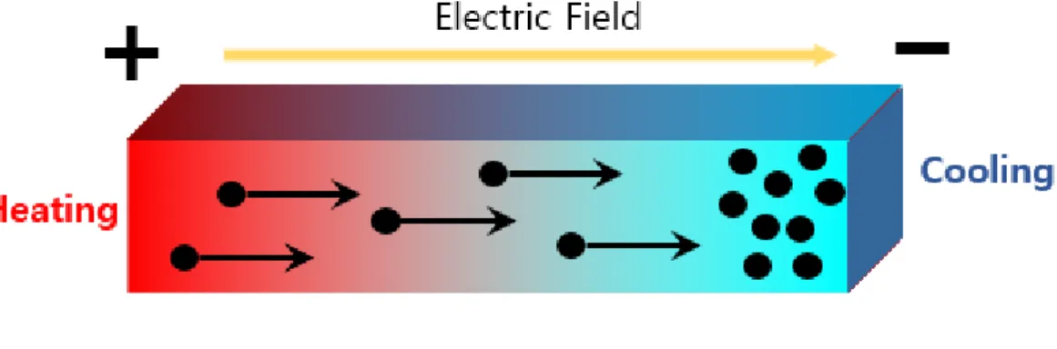
- The Peltier effect
- The Thomson Effect
- Evaluation of thermoelectric materials
The ZT values are proportional to the square of the Seebeck coefficient and the electrical conductivity and are inversely proportional to the thermal conductivity. The thermal conductivity (𝑘) comes from two parts consisting of electron and phonon components. 1.7) The electron term is related to the σ via the Wiedemann-Franz law. According to the Wiedemann-Franz law, it is impossible to independently control the electron contribution of thermal conductivity and electrical conductivity.
Thermoelectric materials
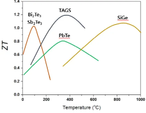
- Characteristic of Bismuth-Telluride material
- The strategies to enhance the ZT value
The crystal structure of the PGEC materials exhibits a large cage-like void with massive atoms (rattling atoms) that result in a phonon damping effect that can extremely reduce the thermal conductivity of the lattice. Although the electrical conductivity was reduced to some extent, the thermal conductivity was reduced more significantly in the bulk ingot of the same material. Several methods have been attempted to improve the performance of n-type TE materials by controlling the number of hot press or spark plasma sintering operations.
Thermoelectric device
- Evaluation of thermoelectric device
- Various types of thermoelectric materials and devices
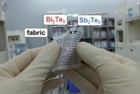
Generally, the conventional TE device has a planar structure with several n- and p-type legs which will be limited when applied to uneven niche heat source. The flexible or wearable TE device stands out as a new type of device that solves the problem. Therefore, it is essential to create the various forms of conventional TE materials and processes, such as screen printing, inkjet printing, lithography, vacuum deposition, CNT composites, PEDOT (3,4-ethylenedioxythiophene): PSS (polystyrene sulfonate), PANI and so on. . at 30.
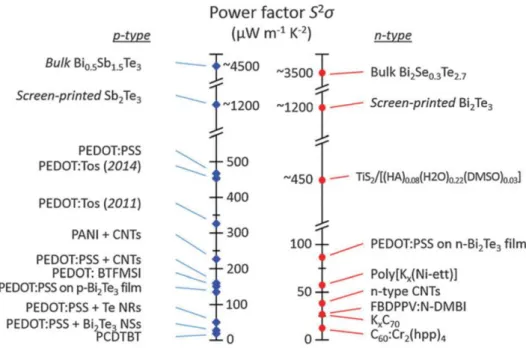
The figure 1.17 shows the characteristic of newly emerging TE materials as used screen printing process which indicated lower PF than bulk material due to low electrical conductivity which has glass dust or polymer binder. Those additives were effectively used to bind the TE microparticles, but the impurities also blocked the charge transport, resulting in significantly reducing the electrical conductivity. In other case, PEDOT: PSS is the most used organic-based TE material which has a good flexibility, air stability, and electrical conductivity.
So far, we have briefly reviewed the development of TE materials through intra-unit cell complexity, nanostructuring, low dimensionality, and defect control with a wide frequency range, which would lead to highly efficient TE materials and fabrication of various TE devices. In recent years, wearable and flexible TE applications have emerged as an efficient way to obtain energy. However, the power density of wearable and flexible TE applications is lower than most, so we need to gather information on how to develop shapeless heat sources and new fabrication methods for TE devices.
Experimental study of the effect of quantum well structures on the thermoelectric figure of merit.
High performance thermoelectric painting
- XPS and XRD analysis of Sb 2 Te 3 -based chalcogenidometalate
- DSC and TGA analysis of Sb 2 Te 3 -based chalcogenidometalate
- Applicability of Sb 2 Te 3 -based chalcogenidometalate solution in various solvents
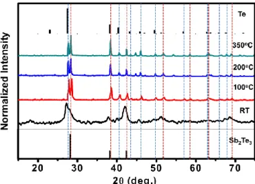
ChaM separates into two phases during heat treatment at 100 oC (red color), 200 oC (blue color) and 350 oC (green color) with the formation of crystalline phases Sb2Te3 and Te. The peaks corresponding to the Sb2Te3 and Te phases in the XRD pattern were more prominent when heated at higher temperatures. Vertical dashed red and blue lines indicate Te and Sb2Te3 samples, respectively.
Dark cyan and navy blue lines indicate heat flux and weight loss, respectively. The result showed that the TGA scan of the dried Sb2Te3 ChaM sample at room temperature shows negligible weight loss up to 450 oC, which is consistent with previously reported Sb2Te3-based chalcogenidometalate8. The endothermic peak in the DSC curve at approximately 420 oC corresponds to the melting point of a Te phase formed from the Sb2Te3 ChaM.
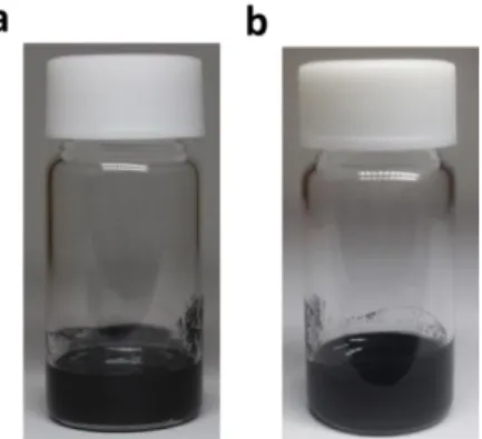
Sb2Te3-ChaM was dispersible in various polar solvents with dielectric constant (ε) ranging from 10 ~ 50, including dimethyl sulfoxide (ε ≈ 47), dimethylformamide (ε ≈ 36), and ethylenediamine (ε ≈ 13) and viscous polar solvents of ethylene glycol ( ε ≈ 37) and glycerol (ε ≈ 43), which made it possible to tailor the properties of TE paints in terms of dielectric constant, solvent viscosity and evaporation temperature. a) Photographs and (b) UV-visible absorption spectra of the Sb2Te3ChaM dispersed in dimethyl sulfoxide (DMSO), dimethylformamide (DMF) and ethylenediamine (En) solvents.
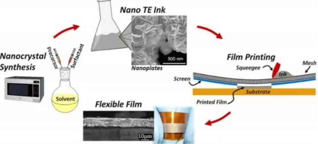
Characterize of thermoelectric ink
- The effect of addition with the Sb 2 Te 3 as a sintering aid
- Thermoelectric properties of n-and p-type sintered sample
The electrical conductivity of the n- and p-type samples gradually decreased as the ambient temperature increased to 125 oC, indicating metallic conductive behavior. Temperature dependence of calculated thermal conductivities in the lattice of n- and p-type painted samples using the modified effective medium theory formulation. The internal resistances of TE devices on convex and concave surfaces were identical values of ∼20 Ω, which was consistent with those of the painted TE devices on planar substrates.
The comparative simulation study was investigated on the power output of the painted TE generator and the conventional module on a curved heat source using COMSOL. The model calculates the temperature distribution and the generated power of the TE generators integrated with a heated hemispherical alumina substrate. The TE generator consists of a pair of n- and p-types of TE layers and conductive paste layers, where the thickness was assumed to be 50 m. Based on the geometry and material properties, the electrical resistance was estimated to be 3.5 per pair of the TE layers.
The output power density of the hemispherical generator is calculated assuming the same dimensions of the TE legs as the others. The fact that the output power density of TE devices painted on flat and curved substrates with the same dimension of TE legs converge on the same line proves the applicability of TE paints on surfaces of any shape. Furthermore, the through-plane TE generator is fabricated using cast discs prepared from TE inks. The significant sintering effects in TE inks work not only for 2D thick films at the μm scale, but also for 3D blocks at the mm scale.
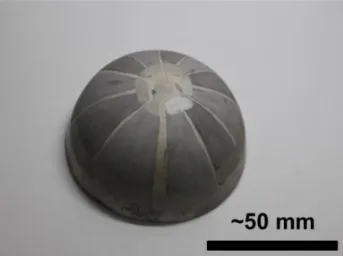
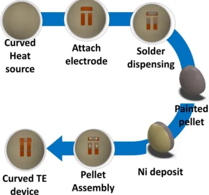
Two pairs of n- and p-type shaped disks with the diameter of 4.0 mm and thickness of 1.0 mm were assembled by soldering with a Bi-Sn solder to Cu foil electrodes on an alumina hemisphere (Figure 2.37). The top sides of TE disks were electrically connected to Cu foil electrodes by soldering, which produced the through-plane TE generator on a hemisphere. The Seebeck coefficient was calculated based on the slope of the voltage versus temperature difference curves. In summary, I report the first successful demonstration of the concept of TE dyeing using molecular Sb2Te3-ChaM-assisted all-inorganic TE dyes.
Fabrication of in-plane type thermoelectric device via Painting process
- The process of thermoelectric painting
- Output characteristics of in-plane thermoelectric devices on flat substrate
- Output characteristics of in-plane thermoelectric devices on curved substrate
Fabrication of hemispherical thermoelectric device via Painting process
- Simulation study on the power output
- Output characteristics of hemispherical thermoelectric devices
Each triangular TE layer has a width of 20 mm and a height of 60 mm so that the substrate has enough surface area for 5.5 pairs of TE layers. The conductive paste was assumed to have a thermal conductivity of 9 W m-1·K-1 and an electrical conductivity of 103 S cm-1. Based on the study of material properties and geometry for commercial TE modules, it was determined that a standard TE module has a substrate area of 40 mm 40 mm and ~100 pairs of Bi-Te materials.
The considered module has a thermal conductivity of 0.65 W K-1, the electrical resistance of 2.3 and the Seebeck coefficient of 52.8 mV/K. For the simple modeling, the FEM for the conventional module includes only one leg of TE material. The temperature distribution of the conventional module is very uneven (Figure 2.31), since the contact area (d) with a hemisphere is narrow, resulting in a significantly low output voltage of 13.3 mV for d = 1 mm and 4.5 mV for d = 0.1 mm.
Thus, conventional module generates an output power of 76.9 W and the output power density of 15 W cm-2 when d = 1 mm. On the other hand, the temperature distribution of a hemispherical module was kept at 45 oC and 25 oC (Figure 2.32), the uniform temperature distribution and the electric potential field of the painted generator result in an order of magnitude higher power density of 205 W cm-2. Slightly lower output voltage than other devices may come from the deviation between the actual temperatures applied to TE pins and temperatures on the hot and cold sides due to heat loss resulting from a small contact area of TE devices to the hot side.
Although this hemispherical TE device showed lower output power density due to large TE layers, these results confirm that TE painting process facilitated shape engineering of TE materials on any-shaped surfaces while maintaining their high TE performance, which is most should be effective heat energy collection from any heat sources.
Fabrication of through-plane type thermoelectric device using molding process
- The process of through-plane type thermoelectric device
- Output voltage and power density of the through-plane thermoelectric device
These results clearly demonstrate the feasibility of the paint technology in terms of TE performance and workability.
Experimental details
- Synthesis of Bi 2 Te 3 -based inorganic thermoelectric paints
- Thermoelectric properties measurement
- Measurement of thermoelectric power generation
To obtain the temperature-dependent Seebeck coefficients, the open-circuit voltage and temperature gradient were measured with two T-type thermocouples using a Keithley 2400 source meter and a Keithley 2000 multimeter. The measuring device rested on a hot plate, and the measurement temperatures were controlled by heating the hot plate. The applied powers of the TE modules in contact with the samples were adjusted to take advantage of the temperature differences.
This arrangement was confirmed by measuring the electrical conductivity and Seebeck coefficient of n-type Bi2Te3 and p-type BiSbTe rod samples, and the accuracy was within ±3%. The thermal diffusivities were measured in a temperature range from 300 oC to 450 oC using laser flash analysis (LFA 457, Netzsch). Carrier concentration and mobility were measured with a Hall measurement system (BIO-PAD, HL5500PC) at room temperature.
The performance of the TE current generator was investigated by measuring the I-V curve and the output power density under temperature differences across the devices using a home-built setup. The temperature differences were measured by two T-type thermocouples in contact with hot and cold sides using Keithley 2000 multimeter. Two Ag electrodes in prepared TE generators were connected to Keithley 2400 source meter and the I-V characteristics were measured using Lab trace 2.0 software (Keithley Instrument, Inc) under desired temperature differences.
The output power density (output power per unit area) was calculated with total cross-sectional areas of TE layers.

Conclusion
A comparative study of spark plasma sintering (SPS), hot isostatic pressing (HIP) and microwave sintering techniques on p-type Bi2Te3 thermoelectric properties.