HIGH SPEED ADDER
Dagrious Anak Jihob
Bachelor of Engineering with Honours (Electronics and Telecommunications Engineering)
2008/2009
UNIVERSITI MALAYSIA SARAWAK
R13a BORANG PENGESAHAN STATUS TESIS
Judul: HIGH SPEED ADDER
SESI PENGAJIAN: 2008/2009
Saya DAGRIOUS ANAK JIHOB
(HURUF BESAR)
mengaku membenarkan tesis * ini disimpan di Pusat Khidmat Maklumat Akademik, Universiti Malaysia Sarawak dengan syarat-syarat kegunaan seperti berikut:
1. Tesis adalah hakmilik Universiti Malaysia Sarawak.
2. Pusat Khidmat Maklumat Akademik, Universiti Malaysia Sarawak dibenarkan membuat salinan untuk tujuan pengajian sahaja.
3. Membuat pendigitan untuk membangunkan Pangkalan Data Kandungan Tempatan.
4. Pusat Khidmat Maklumat Akademik, Universiti Malaysia Sarawak dibenarkan membuat salinan tesis ini sebagai bahan pertukaran antara institusi pengajian tinggi.
5. ** Sila tandakan ( ) di kotak yang berkenaan
SULIT (Mengandungi maklumat yang berdarjah keselamatan atau kepentingan Malaysia seperti yang termaktub di dalam AKTA RAHSIA RASMI 1972).
TERHAD (Mengandungi maklumat TERHAD yang telah ditentukan oleh organisasi/
badan di mana penyelidikan dijalankan).
TIDAK TERHAD
Disahkan oleh
(TANDATANGAN PENULIS) (TANDATANGAN PENYELIA)
Alamat tetap: D3-3B, Demak Laut Commercial Centre, Jln Bako, 93050
Kuching, Sarawak ENCIK NURHUZAIMIN JULAI
Nama Penyelia
Tarikh: 6 APRIL 2009 Tarikh:
CATATAN * Tesis dimaksudkan sebagai tesis bagi Ijazah Doktor Falsafah, Sarjana dan Sarjana Muda.
** Jika tesis ini SULIT atau TERHAD, sila lampirkan surat daripada pihak berkuasa/organisasi berkenaan dengan menyatakan sekali sebab dan tempoh tesis ini perlu dikelaskan sebagai SULIT dan TERHAD.
This Final Year Project attached here:
Title : High Speed Adder Student Name : Dagrious Anak Jihob
Matric No : 13923
has been read and approved by:
__________________________ ______________________
Mr. Nurhuzaimin Julai Date (Supervisor)
HIGH SPEED ADDER
DAGRIOUS ANAK JIHOB
This project is submitted in partial fulfilment of
The requirements for the degree of Bachelor of Engineering with Honours (Electronics and Telecommunications Engineering)
Faculty of Engineering
UNIVERSITI MALAYSIA SARAWAK 2008/2009
Dedicated to my beloved parent, family members and friends who was supported and encouraged me
Thank you for all the support and encouragement
ii
ACKNOWLEDGEMENT
First of all, I would like to thank God, with His guidance and wishes that this final year project can be completed successfully. I also wish to express my sincere gratitude to my project supervisor Encik Nurhuizaimin Julai for his excellent patience, guidance, advice and valuable experience throughout this project.
In particular, I wish to express my appreciation towards the other electronics lecturers, and staff of the Faculty of Engineering, UNIMAS for contributed their commitment, their bright ideas, their valuable time, and their energy towards the development of this project.
Finally, I would like to express my greatest appreciation to my friends, my girlfriend, course mates and my lovely family for their constant cooperation, encouragement, understanding, and supports.
iii
ABSTRAK
Terdapat beberapa jenis kumpulan rekaan penambahan di bawah keluarga rekaan penambahan berkelajuan tinggi. Setiap kumpulaan ada kelebihan dan kebaikan tersendiri. Untuk projek ini, tiga ciri-ciri penambah berkelajuan tinggi akan di bandingkan dan dinilaikan dari segi saiz bit, keluasan rekaaan dan perlengahan masa.
Matlamat projek ini adalah untuk mereka salah satu kumpulan dari keluarga penambahan berkelajuan tinggi menggunakan perisisan komputer yang berkaitan. Jadi, kemampuan untuk cara mencipta Penambahan Berkelajuan Tinggi yang dipersembahkan dalam projek ini akan dibuktikan. Kepekaan dalam perlengahan masa untuk membezakan proses dan pelbagai persekitaran telah disentuh dengan lebih lanjut dalam perlaksanaan keputusan. Oleh itu, daripada keputusan eksperimen menunjukkan bahawa elemen Penambah Berkelajuan Tinggi mampu memberikan jumlah perlengahan masa yang dapat diterima tanpa menggunakan kuasa yang besar. Dengan itu, daripada perbandingan keputusan yang akan ditunjukkan dalam projek ini nanti akan membuktikan bahawa memilih elemen perlengahan masa yang terbaik adalah sangat berguna untuk diaplikasikan di mana keperluan dalam bentuk masa itu sendiri beroperasi ke arah rekaan penambahan berkelajuan tinggi.
iv
ABSTRACT
There are various group of adder design under high speed adder family design.
Each group has its own advantages and disadvantages. For this project, three important criteria of high speed adder will be compared and analyzed: bit size, design’s area, and propagation delay. The aim of this project is to design one group member of high speed adder’s family using related software. Thus, the capability for the methodology by designing the Brent Kung Adder(s) is presented in this project by which to proven. The sensitivity of the delay elements to different process and environmental variations is studied from the simulation results. Therefore, the experimental result represent that the high speed adder elements gave a reasonable amount of delay without large power costs.
So, from the comparison results presented in this project will prove useful for selecting the best delay element to apply which is the essential part for self-timed operation in high speed adder.
i
TABLE OF CONTENTS
Content Page
Dedication i
Acknowledgement ii
Abstrak iii
Abstract iv
Table of Contents i
List of Tables v
List of Figures vi
List of Abbreviations ix
CHAPTER 1: INTRODUCTION
1.0 Background 1
1.1 Objectives of Project 3
1.2 Project Outline 4
1.3 Thesis Outline of Project 5
CHAPTER 2: LITERATURE REVIEW
2.0 Introduction 7
2.1 Half Adder 8
2.2 Full Adder 10
ii
2.3 Ripple Carry Adder 13
2.4 Carry Look-Ahead Adder 15
2.5 Parallel Prefix Adder 17
2.6 Kogge-Stone Adder 21
2.7 Brent-Kung Adder 23
2.8 Brent Kung Adder Ideology Design 25 2.8.1 Propagate-Generate –Block 27 2.8.2 Fundamental Carry Operator 28
Block
2.8.3 Parallel Prefix Carry Block 30 2.8.4 Parallel Prefix Sum Block 31 2.8.5 BKA design for 8-bit and 32
16 bit word length
2.8.6 BKA design for 32-bit length 35 2.8.7 BKA design for 64-bit length 36
2.9 Design Sofware 36
CHAPTER 3: METHODOLOGY
3.0 Project Process Flow 38
3.1 Project Design Flow 40
3.1.1 Design Entry Project 41 3.1.2 Generate VHDL source code 41
3.1.3 Compilation 44
3.1.4 Simulation 44
iii
3.1.5 Analysis and Synthesis 45 3.1.6 Modification and Implementation 45
Process
CHAPTER 4: RESULTS, ANALYSIS & DISCUSSIONS
4.0 Discussion on BKA-8, BKA-16, BKA-32 46 and BKA-64 bit design
4.2 BKA-8 bit simulation functional waveform 47 results
4.3 Discussion on BKA-8 bit simulation functional 48 waveform results
4.4 BKA-16 bit simulation functional waveform 49 results
4.5 Discussion on BKA-16 bit simulation functional 50 waveform results
4.6 BKA-32 bit simulation functional waveform 51 results
4.7 Discussion onBKA-32 bit simulation functional 52 waveform results
4.8 BKA-64 bit simulation functional waveform 53 results
4.9 Discussion on BKA-64 bit simulation functional 54 waveform results
4.10 Results of BKA n-bit timing analysis 58
iv
4.11 Discussion on the BKA n-bit timing analysis 60 results
4.12 Problem Encounter 64
4.13 Problem Solution 64
CHAPTER 5: CONCLUSION AND RECOMMENDATION
5.0 Conclusion 65
5.1 Future Work 68
5.2 Recommendation 69
REFERENCES 70
APPENDIX 74
v
LIST OF TABLES
Table Page
Table 2.1: HA truth table 10
Table 2.2: FA truth table 13
Table 4.1: Comparison between BKA ‘n’-bit versus internal blocks 46 Table 4.2: Representative values of Decimal, Hexadecimal and Binary 54 Table 4.3: Comparison between worst case propagation delays of 61
BKA bit size designed
vi
LIST OF FIGURES
Figure Page
Figure 1.1: Datapath Bit-Sliced Organization in IC designs 2 Figure 1.2: Evaluating High Speed Adder Block Diagram 6
Figure 2.1: HA Structure 8
Figure 2.2: Schematic HA gate logic 9
Figure 2.3: FA structure 11
Figure 2.4: Schematic FA gate logic 12
Figure 2.5: RCA structure 14
Figure 2.6: Calculation with carry operation 15
Figure 2.7: CLA structure 16
Figure 2.8: PPA derivation Block Diagram 17
Figure 2.9: Parallel prefix product with prefix operator (€) 19
Figure 2.10: PPAs network example 21
Figure 2.11: Basic structure of 16 bit radix-2 KSA 22 Figure 2.12: Basic structure of 16 bit radix-2 BKA 24 Figure 2.13: BK Prefix Parallel computation structure 26
Figure 2.14: Schematic view of PG block 28
Figure 2.15: Schematic View of FCO block 29
Figure 2.16: Schematic View of ppC block 31
vii
Figure 2.17: Schematic view of ppS block 32
Figure 2.18: BK-PPA design for 8-bit length 33
Figure 2.19: BK-PPA design for 16-bit length 34
Figure 2.20: BK-PPA design for 32-bit length 35
Figure 2.21: BK-PPA design for 64-bit length 36
Figure 3.1: Project Flow Chart 39
Figure 3.2: The Design Flow of each project stage 40 Figure 4.1: BKA-8 bit simulation functional waveform results 47 Figure 4.2: Sample from BKA-8 bit simulation waveform 48 Figure 4.3: BKA-16 bit simulation functional waveform 49 Figure 4.4: sample from BKA-16 bit simulation waveform 50 Figure 4.5: BKA-32 bit simulation functional waveform results 51 Figure 4.6: sample from BKA-32 bit simulation functional 52 Figure 4.7: BKA-64 bit simulation functional waveform results 53 Figure 4.8: Sample from BKA-64 bit simulation waveform 56 Figure 4.9: Sample from BKA-64 bit simulation waveform 57 Figure 4.10: BKA 8-bit worst-case propagation delay 58 Figure 4.11: BKA 16-bit worst-case propagation delay 58 Figure 4.12: BKA 32-bit worst-case propagation delay 59 Figure 4.13: BKA 64-bit worst-case propagation delay 59 Figure 4.14: BKA bit size versus worst-case propagation delay 62 Figure 4.15: Graph of BKA n-bit stages versus propagation delay 63 Figure 5.1: High Speed Adder design derivation Block Diagram 66
ix
LIST OF ABBREVIATIONS
IC - Integrated Circuits
CPU - Central Processing Unit ALU - Arithmetic Logic Unit HSA - High Speed Adder
FA - Full Adder
HA - Half Adder
RCA - Ripple Carry Adder CLA - Carry Lookahead Adder PPA - Parallel Prefix Adder BKA - Brent Kung Adder KSA - Kogge-Stone Adder
Ci - Carry in
Co - Carry out
S - Sum
PFA - Partial Full Adder
Gi - Generates function
Pi - Propagate function
L - Number of lookahead levels in the design FPGA - Field-Programmable Gate Array
LUTs - Slice Look-Up Tables
x
€ - Carry Operator
PG - Propagate-Generate function FCO - Fundamental Carry Operator ppC - parallel prefix Carry
ppS - parallel prefix Sum
CPLD - Complex Programmable Logic Devices EDA - Electronic Design Automation
LPM - Library of Parameterized Modules IP - Intellectual Property
EDIF - Electronic Design Interchange Format SDC - Synopsys Design Constraint
GUI - Graphical Unit Interface
SRAM - Random Access Memory
tpd - Propagation delay
1
CHAPTER 1
INTRODUCTION
1.0 Background
Computers, mobile phones, gaming devices or consoles, mp3 players, televisions, digital cameras, digital watches and ATM machine are the few types of technology that may came across almost every day. This technology operates with functions of the Central Processing Unit (CPU) or some of it may as simple Integrated Circuits (IC). Generally, the very basic component of either CPUs or ICs is the adder.
The search for hardware algorithms for addition has been started around year 1950. The addition function is the most basic and commonly used arithmetic operation in our life. In terms of digital electronic engineering, adder is a device that will perform the additional operation. Adder is a part of Arithmetic Logic Unit (ALU) in the computer and some ALUs may consist of multiple adder. Adder performs addition operation by using interior combination of primitive logic gate inside adder itself.
2
Although adder can be constructed in many other numerical representation but basically in computation adder is operated on the binary representation.
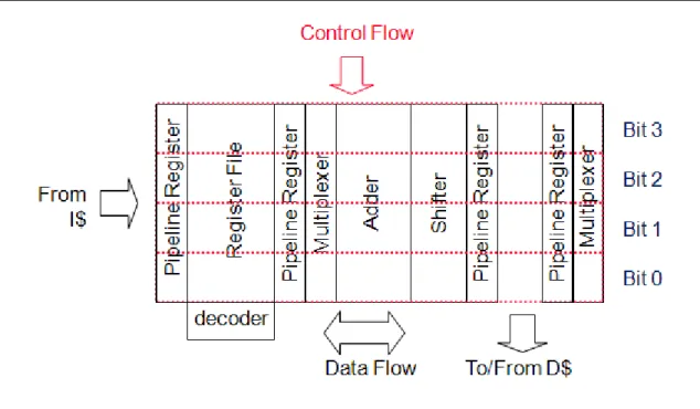
As shown in Figure 1.1, the datapath of IC design, one of the very basic structure implemented in IC design in Adder. Adder is widely used in the generic computer [2]
for the reason that it is very important for adding data in the processor. The processing speeds of one’s computer turn out to be the most considerable requirement acquired by ones technology users.
Figure 1.1: Datapath Bit-Sliced Organization in IC designs
3
In general, the purpose of adder designed is to strive with the Sum operation of the Arithmetic Logic Unit (ALU). This operation is then applied to other arithmetic operation such as: the subtraction, multiplication and the division function. These were very basis operation in order to constructs programs which later are derived into more advance and complex programs which alter into all technology which have been seen nowadays. The performance and the reliability is the main key in order ones technology to be acknowledge these days. As time passed by, the technology operation needs to undergo with smoothly and efficiently. Time is Gold, even a delay of 1 second could cost gargantuan losses, therefore to human always rushing for time, especially for technology devices user, always demanding for the faster speed of technology.
1.1 Objectives of Project
Following are the objective of this project;
1. To design a group of adder which are belongs to High Speed Adder family 2. To design the High Speed Adder group with Quartus II program.
3. To designs and simulates several bit size of High Speed Adder.
4 1.2 Project Outline
The target of this project is to design a High Speed Adder with Quartus II Web Edition Version 8 program. The Quartus II program is chosen because it includes all of the design files, software source files, plus other related files that necessary for the eventual implementation of a design in a programmable logic device.
Figure 1.2: Evaluating High Speed Adder Block Diagram
Since there are various type adder design categorize as High Speed Adder, relevant evidence are acquired via comparing and evaluating each adders design in the following viewpoint; intentional output speed, delay, bit size and area. The involvement of bit size will concern in term of cost nowadays. The speed of the output and the delay
High Speed Adder
Viewpoint
Speed Delay Bit Size Area
5
point of view isthe verification of performance and the value of the design. While, bit size are the requirement aspect in performance view whereas the design area is a factor of reliability revelation.
As well, the circuitry design areas are also anxiety of the all cost design. All these criteria agonize whether it worthwhile to acknowledge as HSA as well in the price market nowadays. Afterward all the characteristics of high speed adders are compared and the ones with greater advantage is agonize as HSA.
1.3 Thesis Outline of Project
This project is divided into 5 chapters in general and is prearranged as follows:
Chapter 1 of this project report are discusses on the introduction of the Adder operation and the overview of the various types of adder design. In addition, this chapter stated clearly the type of adder design to be research on. Plus, it also included a viewpoint of the adder to be designs. Furthermore, the objective of this project will be included to give a clear view and information needed.
Chapter 2 is the literature review of this project. There various type of High Speed adder design as High speed adder is design stage by stage, starting with HA or FA
6
design stage until PPA design stage. Each design stage is review in the chapter. The characteristics of a good performance of the High Speed Adder included.
Chapter 3 discusses the study of one type of High Speed Adder; it includes the algorithm of the High Speed Adder. In addition, this chapter also contains the performance comparison of each adder designed. Furthermore a revision method that used in Chapter 1 and 2 is also included. Plus, the methodology of designing project is also affirmed.
Chapter 4 contains the simulation results and a discussion which is comparison and analysis of the delay element are made. Concern the approach and analysis to achieve the objectives.
Chapter 5 concludes and summarizes the overall process and performance of the project. In addition, further work which can be implemented or improve the project is also being discussed for future improvement.