Questions regarding the use of the book should be directed to the Rights and Permissions Department of INTECHOPEN LIMITED ([email protected]). Peng He is the acting director of the State Key Laboratory of Advanced Welding and Joining, China.
121 Plastic Inorganic Semiconductors for Flexible Electronics
Introduction
One of the most exciting research fields in recent decades in the field of materials engineering is that of hybrid nanomaterials. These materials possess extraordinary physical and chemical properties derived from their size in the nanoscale.
Basic concepts
The development of multifunctional applications has received a lot of attention in the last two decades thanks to the chemical and physical properties of the materials, which give rise to developments with a high added value. In addition, the chemical nature of the components and the interaction between them leads to different possibilities of structure, degree of organization and properties.
Classification
A second class of hybrid materials are those based on the synergy of the phases through strong chemical bonds such as Lewis acid-base, covalent or ionic-covalent bonds. In addition, hybrid materials can be classified as organic-in-inorganic (organic parts used to modify inorganic materials) or inorganic-in-organic (inorganic components used to modify organic materials or matrices), as illustrated in Figure 3 [3].
Applications
Types of hybrid materials based on the addition of inorganic and organic components and vice versa. A wide variety of hybrid materials have been proposed for implementing electrodes for rechargeable batteries using inorganic polymers and materials such as graphene, carbon nanotubes or a combination thereof [8].
Conclusions
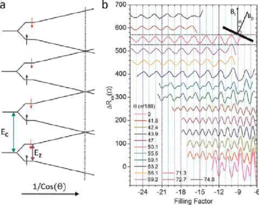
Hierarchy of hybrid materials - The place of inorganic-in-organic substances in it, their composition and applications. Besides the formation of LLs, the energy of the electron is also split by the Zeeman effect EZ¼gμBB, where μB¼ eℏ=2m0 (m0 is free electron mass) is the Bohr magneton and g is the Landé g-factor.
High-quality FET based on BP
- Realization of air-stable devices based on BP
- Ohmic contact and ambipolar transport in BP
- Strong transport anisotropy in BP
- Widely tunable electronic bandgap
As soon as devices can be manufactured with high enough quality, we move to the electronic transport in quantum limit (cryogenic temperature and high magnetic field). For practical applications, the dynamic bandgap tuning can be realized by the dual-gate FET configuration in BP-based devices [37].
SdH oscillation and quantum hall effect in BP
Surprisingly, this selective area etching technique can be effectively applied to other 2D semiconductors such as high performance TMDCs [28]. Based on this screening effect, wide quantum wells have been formed in few-layer BP, which can be switched between double layers of charge carriers and single layers of charge carriers [55].
Conclusions
Avsar A, Vera-Marun IJ, Tan JY, Watanabe K, Taniguchi T, Castro electron transport in few-layer black phosphorus. Transport properties of pristine few-layer black phosphorus by van der waals passivation in an inert.
Preparation techniques of three-dimensional nanocarbon hybrids Up to now, varied approaches have been used for the fabrication of 3D nanocar-
- Mixing process of surface-treated carbon materials
- Hydrothermal method
- Multi-step approaches using combinations of decorated carbon materials and CVD
- Multi-step synthesis by chemical vapor deposition
- One-step synthesis by chemical vapor deposition
To date, a number of techniques and methods have been used for nanocarbon hybrid fabrication, such as the mixing process of surface-treated carbon materials (including solution processing [31, 32], vacuum filtration [33, 34], - by-layer self-assembly method, hydrothermal method [37 ], multi-step approaches with combinations of decorated carbon materials and CVD [10], and multi-step and one-step chemical vapor deposition [38-48].3-dimensional nanocarbon hybridsTo date, several approaches have been used for the fabrication of 3D nanocar-.
Effect of experimental parameters of CVD methods 1 Effect of catalyst nanoparticles
- Effect of growth temperature
- Effect of carrier gas
- Effect of carbon source
Furthermore, the growth temperature is also crucial for the defects and properties of 3D carbon nanomaterials. In the CVD approach, hydrogen (H2), argon (Ar) and nitrogen (N2) are used to grow carbon materials in a high temperature annealing process and.
Development trend and application prospect of three-dimensional nanocarbon hybrids
- Three-dimensional nanocarbon hybrids in transparent and flexible electrodes and field-effect transistors
- Three-dimensional nanocarbon hybrids in fuel cell and batteries In the practical application, the higher active and stable catalysts are crucial
- Three-dimensional nanocarbon hybrids in supercapacitors
Synthesis of three-dimensional nanocarbon hybrids by chemical vapor deposition DOI: http://dx.doi.org/10.5772/intechopen.89671. It is no doubt that 3D nanocarbon hybrids will have a decisive impact on the emerging materials of high-performance supercapacitor applications.
Conclusion and further prospects
A simple approach to the fabrication of graphene-carbon nanotube hybrid films on a copper substrate by chemical vapor deposition. Synthesis of three-dimensional carbon nanotube/graphene hybrid materials by a two-step chemical vapor deposition process.
Ion exchangers
- Inorganic ion exchangers
- Organic ion exchangers
- Hybrid ion exchangers
- Hybrid metal phosphates
This new class of ion exchangers has been prepared in these laboratories by incorporating a polymeric or monomeric organic species into the inorganic ion exchange matrix [26-30]. In the last 10-15 years, some hybrid ion exchange materials have been synthesized in laboratories, such as acrylamide.
Surfactants
- Micelle formation and critical micelle concentration (CMC)
- Surfactant adsorption and surface properties
It is clear from the above discussion that they play an important role in the adsorption behavior of the molecules. Consequently, exceptionally high adsorption of the mentioned metal ions has opened the doors in the field of materials science.
Conclusion
It was considered worthwhile to incorporate the surfactants into the matrix of inorganic ion exchangers to see how they could change the properties of the ion exchangers. They have improved not only the ion exchange capacity of the inorganic metal phosphates when present in their matrix, but also the adsorption of metal ions.
Component of PSA
The demand for thin and flexible displays is increasing as the interest in small and diverse designs grows [8]. The recovery and stress relaxation properties of OCA are important for flexible displays because a high recovery of PSA prevents it from deformation under repeated folding-unfolding conditions [14].
Development in display and OCA
When OCA is directly bonded to ITO film, the acid component must be excluded for the durability of the ITO film. The first step is a synthesis of an acrylic prepolymer by UV irradiation to a mixture of the monomers and photoinitiator.
Stress dispersion and neutral plane
The manufacturing process of the curved display includes the bending process of the OLED panel. So the curved module OCA must have high adhesion properties to withstand this force.
Test methods for foldable OCA
- Shear strain on folded OCA
- Adhesion strength
- Shear modulus
- Shear creep and stress relaxation
One of these limitations is the replacement of the glass cover with a plastic cover for collapsible features [47]. Maintenance of shear modulus ensures bond strength [38], strain recovery, and high temperature machinability.
Researches of OCA for flexible display
In the stress relaxation test, the continued decrease of stress is observed after the highest stress appears in response to the initial rapid deformation (Figure 9). Permanent deformation that cannot be recovered after removing stress in creep and stress relaxation measurement may cause wrinkles or optical defects during the folding test of the display module or final product.
Summary
The effect of the degree of cross-linking is similar to that of acrylic OCA. Effect of stress relaxation property of acrylic pressure sensitive adhesive on light leakage phenomenon of polarizer in liquid crystal display.
Simulation
- Device structure and finite element-based numerical simulation
- Device physical equation
- Density of defect states model
- Trapped carrier density
- Poole-Frenkel mobility model
Also TCAD simulation results and compact modeling results were compared and contrasted with the experimentally measured results of the device. The first three equations are the default equations that ATLAS uses to find the electrical behavior of the device.
Compact modeling, model parameter extraction, and model verification
- Model features
- Model description
- Effective channel mobility
- Intrinsic drain-source current
The power-law dependence of the carrier concentration mobility is determined by the temperature-dependent model parameter GAMMA. Is the ideal intrinsic drain-source saturation current, and the effective channel conductance in the linear region Gchi is obtained in the following way: . where Gch0 is the intrinsic effective conductance of the channel in the linear region and Rdsis is the nonlinear bias dependent series resistance for the channel intrinsic region defined by temperature dependent model parameter RDS and the model parameter VRDS; on the other hand, Weff and Leff are effective channel widths and length, respectively.
Results and discussion
- Material parameters used for DNTT
- Comparison of TCAD-based numerical simulation characteristics and compact model-based simulation characteristics with experimental
- Parameter extraction
- Simulation of logic circuit
Comparisons of transfer characteristics of measured data, TCAD simulated data and modeled data. Comparisons of output characteristics of measured data, TCAD simulated data and modeled data.
![Figure 3 shows the transfer characteristics obtained for the TCAD-based numerical simulation, compact model-based simulation of DNTT-based organic thin film transistor, and the measured characteristic of DNTT-based OTFT [24].](https://thumb-ap.123doks.com/thumbv2/1libvncom/9202276.0/107.765.167.598.83.424/transfer-characteristics-obtained-numerical-simulation-simulation-transistor-characteristic.webp)
Conclusion
The results show that the UOTFT model correctly simulates the behavior of the devices reported in this study and should be used for more complex circuits based on organic thin-film transistors. Different printing techniques based on contact/non-contact approach of printing tools with target substrates have been investigated.
Printed electronic technologies
- Noncontact printing technologies .1 Inkjet material printer
- Contact-based printing technologies
The width-to-depth ratio of the microcells in the gravure cylinder also plays an important role in the manipulation of ink transfer [41]. The surface energy of the stamp and target surfaces play an important role in efficient ink transfer.
Mass production perspective
- Fused deposition modeling
- Stereolithography
- Digital light processing (DLP)
- Selective laser sintering (SLS)
A very thin layer of powder material is then deposited with the aid of a blade normally 0.1 mm thick on the object platform. A very thin layer of powder material is then deposited with the aid of a blade normally 0.1 mm thick on the object platform.
Fundamental concepts: flexibility
Hence, the discovery of the plastic inorganic semiconductor Ag2S [21] at room temperature [21] and the fabrication of all-inorganic Ag2S-based thermoelectric (TE) power generation modules [22] are groundbreaking and open a new path to flexible electronics of the next generation. . We will first clarify the concept of flexibility and then illustrate the intrinsic plasticity for metals and brittleness for inorganic materials.
Prevalent brittleness for inorganic semiconductors
Beyond the characteristics of covalent bonding, the lack of plasticity and flexibility in inorganic materials can be interpreted in terms of dislocations. Various defects exist in inorganic materials (eg, ceramics) such as voids, interstitials, and voids, strongly hindering the movement of dislocations.
Plastic ionic inorganic materials
In addition, grain boundaries can cause dislocation stacking, which can be a type of crack source. For metals, the accumulation of dislocations near grain boundaries will cause hardening of mechanical properties.
Plasticity of ZnS in darkness
Relationship between the GSF energy and the double surface energy of the 2γs plane {001} for different slip systems in NaCl and AgCl. Therefore, the different charge states of the two dislocations in ZnS will lead to a large difference in their mobility, leading to the observed strain twinning.
Room-temperature plastic semiconductor Ag 2 S
The plasticity of Ag2S is extraordinary: engineering strains are ~4.5% in tension, 50% in compression, and above 20%. The distribution of the electron localization indicator (ELI-D) shows a local maximum on the outside of each S atom, and the basin of this maximum is due to lone pair formation or the strong Ag-S interaction shown in the quantum theory of atoms in molecules (QTAIM).
Full inorganic flexible thermoelectric materials
According to the mechanical property test, the ductility and flexibility of Ag2S-based materials will be maintained if the Se content is less than 60% or the Te content is less than 70%. To further verify the robustness of Ag2S-based materials under different usage scenarios, bending cycle test was performed on Ag2S0.5Se0.5 strip with a thickness of about 10 μm.
Summaries and outlook
This chapter reviews emerging plastic inorganic semiconductors (e.g., Ag2S) for next-generation flexible electronics. Plastic Inorganic Semiconductors for Flexible Electronics DOI: http://dx.doi.org/10.5772/intechopen Faber KT, Malloy KJ.
![Figure 3 shows the transfer characteristics obtained for the TCAD-based numerical simulation, compact model-based simulation of DNTT-based organic thin film transistor, and the measured characteristic of DNTT-based OTFT [24].](https://thumb-ap.123doks.com/thumbv2/1libvncom/9202276.0/106.765.116.649.762.987/transfer-characteristics-obtained-numerical-simulation-simulation-transistor-characteristic.webp)
