We will also focus on recent breakthroughs of the MAPLE technique for the fabrication of functional devices, i.e. FTIR spectra of the PIB polymer layer deposited at a laser fluence of 0.1 J/cm2 (for band assignment, see [24]).
Coatings for orthopedic applications
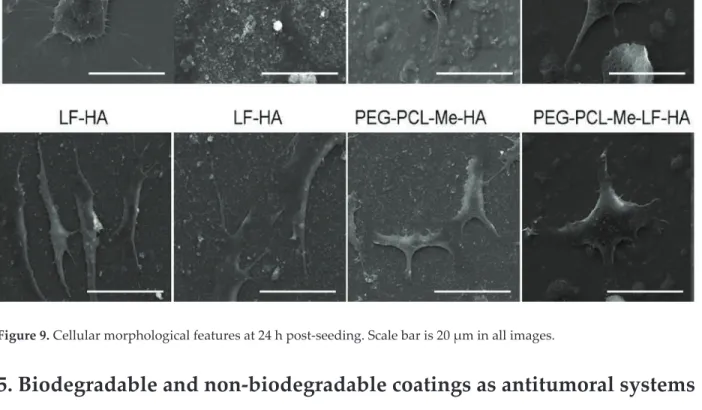
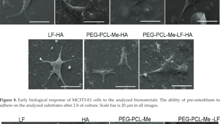
Therefore, by combining various specific features of the compounds of interest with laser parameters to tailor the interface characteristics of the biosurface, the potential of MAPLE for surface modification and engineering is crucial. The great potential of the MAPLE technique in incorporating several bioactive factors into a biodegradable synthetic polymer thin film (PEG-PCL Me) in one step and under vacuum conditions, with minimal influence of solvents or deposition conditions on the functionality of Lf or HA, is the main reason for choosing it as a flexible method for the controlled functionalization of the implant surface in terms of quality, quantity and morphology to promote the survival, proliferation and differentiation of MC3T3-E1 mouse preosteoblasts.
![Figure 7. Experimental setup (a) and target modification (b) from [34].](https://thumb-ap.123doks.com/thumbv2/1libvncom/9201317.0/12.918.136.784.849.1161/figure-experimental-setup-target-modification-b.webp)
Biodegradable and non-biodegradable coatings as antitumoral systems
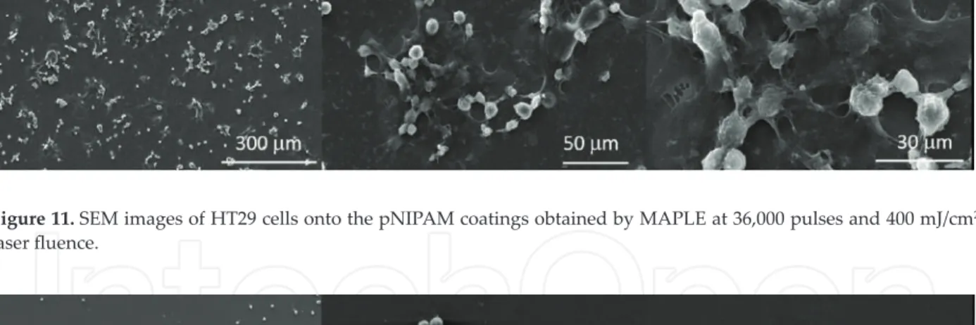
In addition to resistance to the chemotherapeutic effect, drugs such as cisplatin (Cis) can cause a nephrotoxic effect on cells. By combining pNIPAM with the drug dacarbazine, the effect on the tumor cell line HT29 was evaluated.
Conclusions
Acknowledgements
Author details
Acetone and ethanol solid-state gas sensors based on TiO2 nanoparticles thin film deposited by matrix-assisted pulsed laser evaporation. Functionalized polysiloxane thin films deposited by matrix-assisted pulsed laser evaporation for advanced chemical sensing applications. Molecular dynamics simulation study of extrusion and transport of polymer molecules in matrix-assisted pulsed laser evaporation.
The structure of the monomeric pig odor-binding protein sheds light on the domain-swapping mechanism. The protein scaffold of the lipocalin odor binding protein is suitable for the design of new biosensors for the detection of explosive components. Stimuli-responsive interfaces and systems for the control of protein-surface and cell-surface interactions.
Temperature-responsive functional polymeric thin films obtained by matrix pulsed laser evaporation for the study of cell attachment-detachment.
Micro- and Nano-Structuring of Materials via Ultrashort Pulsed Laser Ablation
Introduction
Ultrashort pulsed lasers (USPLs) are a special class of lasers whose pulse duration (tp) is less than a few picoseconds (ps). This classification is based on the fact that for most solids the time to establish thermal equilibrium between electrons and phonons is of the order of picoseconds. In view of the extremely short pulse duration and high intensity, USPLs have been explored and demonstrated great potential for a wide range of applications in physics, chemistry, life sciences, materials and engineering in the last 20 years.
Because of this, a material can be machined very precisely with minimal or even no collateral damage. The advantages of USPL material processing include: (i) high precision [1, 2], (ii) minimal collateral damage, (iii) the ability to process virtually any material, (iv) 3D fabrication [3–5], and (v) a single step to create various surface structures, such as laser-induced periodic surface structures (LIPSS) [6]. In this chapter, three areas of laser material processing are considered: (a) interaction and laser material removal mechanisms, (b) modeling of laser material removal, and (c) applications.
USPL application examples focus on changing material properties below the surface of transparent materials and LIPSS for sensors, precision molds and medical devices.
Mechanisms of laser-material interaction and ablation
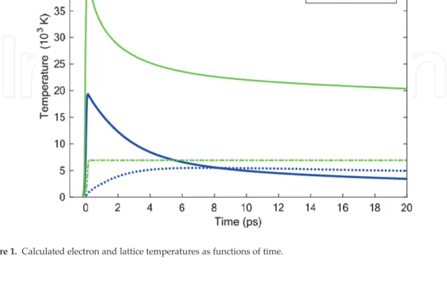
Meanwhile, part of the electron's thermal energy is transferred to the lattice (phonons) by collision between electrons and phonons. Due to the small size of the affected thermal zone, the lattice temperature gradient can be very sharp. For USPL heating at laser impacts slightly exceeding the ablation threshold, only a thin layer of material is ablated by a single pulse due to the effects of the hot electron blast and/or thermal expansion.
For laser fluences well above the ablation threshold, non-thermal ablation occurs only in the early USPL heating time [11]. When a semiconductor or dielectric material is irradiated by a laser, electrons in the valence band absorb photon energy and then enter the conduction band by single- or multi-photon absorption, depending on the photon energy (hv, where Planck's constant and v is the frequency of the laser light) and the band gap energy (Eg) of the material. When the kinetic energy of the excited electron crosses the surface barrier and the momentum component normal to the surface of the material is positive, the excited electrons can escape from the irradiated material into the surrounding air or vacuum.
Fabrication/machining/machining can be performed on the surface or within the bulk of the material by moving the laser focus along the desired paths.
Modeling of laser material ablation
The last term on the right-hand side of Eq. 9) is the hot-electron detonation power. Taking into account the effects of the hot electron ballistic motion [40], the laser heat source is modified to: .. where 1/ is the temperature-dependent optical penetration depth and δb is the ballistic electron penetration depth. Once phase explosion no longer occurs, evaporation can continue until the grid temperature drops significantly. Figure 4 shows the time history of the ablation depth for copper foil irradiated by a single femtosecond laser pulse (duration 120 fs, wavelength 800 nm) of different fluences.
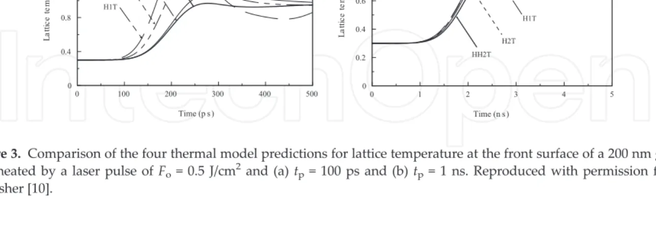
Comparison of four thermal model predictions for the lattice temperature at the front surface of a 200 nm gold film heated by a laser pulse Fo = 0.5 J/cm2 and (a) tp = 100 ps and (b) tp = 1 ns. Based on the relaxation time approximation of the Boltzmann equation, the rate equations are derived for the dynamics of electron-hole carrier density and current, ambipolar energy flux, carrier energy, and lattice energy. For semiconductor materials, the lattice thermal conductivity is comparable to the bulk value.
Modeling of the non-thermal ablation of semiconductor materials via Coulomb explosion can be found in the study by Stoian et al.
Applications
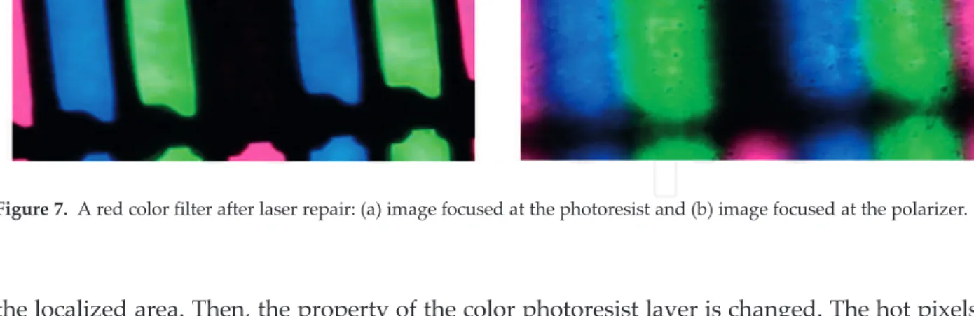
Hot pixels become dead pixels and any defective pixels inside the packaged LCD panel can be directly repaired. Figure 7 shows a red color filter after laser repair. In Figure 7(b) , however, the polarizer corresponding to the red-colored filter (marked with an arrow) is not damaged after laser irradiation. Therefore, the damaged pixel is eliminated by turning the bright one into a dark one.
LIPSS from USPLs allows for a new range of functionalized surface treatments that allow new applications for sensors, medical devices, precision molds, etc. For sensor applications, fabrication of Ag nanostructure-covered surface structures can be used for surface-enhanced Raman scattering (SERS). For precision molding applications, for example, LIPSS of USPLs can be used to fabricate structured molds and rapidly replicate large hierarchical micro/nano structures (lotus leaf-like patterns) on a plastic part by injection molding [54].
Compared to a regular plastic surface, the contact angle of the structured plastic parts increases by 38%, from 97 to 134.
Conclusion
Laser-induced phase explosion: New physical problems when a condensed phase approaches the thermodynamic critical temperature. Morphological and optical characteristics of femtosecond laser-induced large-area micro/nanostructures in GaAs, Si and bronze. Ultrashort-pulse laser ablation of copper, silver, and tungsten: Experimental data and two-temperature model simulations.
Modeling ultrafast phase changes in metal films irradiated with an ultrashort laser pulse using a semiclassical two-temperature model.
Multi-Beam Multi-Target Pulsed Laser Deposition of AZO Films with Polymer Nanoparticles for
Thermoelectric Energy Harvesters
Methods and materials
Two pulsed laser beams simultaneously ablated two targets and ejected the target materials in plumes that propagated toward the surface of a substrate, where they mixed to form a nanocomposite film. Linear actuators tilted the targets and changed the directions of the vanes to ensure uniform mixing of the target materials in the film. The inorganic AZO target was a pellet of Zn0.98Al0.02O, where the aluminum fraction was 2% of the total weight compared to zinc, excluding the oxygen.
The MAPLE target was a solution of PMMA in chlorobenzene at a ratio of 1 g solids per 10 ml liquids filtered with 0.2 μm filter. The solution was poured into a copper cup of the MAPLE target assembly (Figure 3) and frozen in liquid nitrogen (LN). The fluence varied from 0.84 to 2.4 J/cm2 per pulse to maintain a volume fraction of PMMA in the AZO matrix of about 5%.
The thickness of the deposited films was approximately 150 nm as measured with an atomic force microscope.
Results and discussion
Furthermore, the thermal conductivity of the films was measured at 300 K using the time domain thermoreflectance (TDTR) technique [23, 24]. The electrical conductivityσ of AZO + PMMA films is higher than that of the AZO films over the whole measured temperature range and increases with the increase in temperature (Figure 6). Temperature dependence of the electrical conductivity of AZO and AZO + PMMA films deposited on Al2O3.
The PF value for AZO + PMMA films (Figure 8) was found to be higher than that of AZO thin films due to higher electrical conductivity. Temperature dependence of the power factor of AZO and AZO + PMMA thin films on Al2O3 substrates. This is due to the higher electrical conductivity and lower thermal conductivity of the nanocomposite film.
Temperature dependence of the thermoelectric figure of merit Z of AZO and AZO + PMMA thin films on Al2O3 substrates.
Conclusions
Pyrolysis leading to the carbonization of polymers, such as PMMA, poly(vinylidene fluoride)-PVDF, poly(acrylonitrile)-PAN and poly-N-vinylformamide-PNVF, during laser ablation and thermal treatment has been previously reported and used to modify the electrical conductivity of polymeric coatings and fibers [3-3]. In the case of AZO + PMMA films, carbonization can turn the network of polymer nanoclusters and nanofibers into an additional efficient passage for electric current (Figure 12) contributing to the overall increase in electrical conductivity of the nanocomposite films and ultimately to the increase in ZT. Dual-beam pulsed laser deposition of composite films of poly(methacrylate) and rare earth fluorine conversion phosphors.
Polymer-inorganic nanocomposite thin-film upconversion light emitters prepared by double-beam matrix assisted pulsed laser evaporation (DB-MAPLE) method. Ammonia sensor based on polymer-inorganic nanocomposite thin-film upconversion light emitter prepared by double-beam pulsed laser deposition. Polymer nanocomposite films with inorganic up-conversion phosphor and electro-optical additives made by simultaneous triple-beam matrix-assisted and direct pulsed laser deposition.
Tuning the electrical properties of hierarchically assembled Al-doped ZnO nanorods by pulsed laser deposition at room temperature.
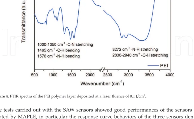
![Figure 3. FTIR spectra of the PIB polymer layer deposited at a laser fluence of 0.1 J/cm 2 (for band assignment, see [24]).](https://thumb-ap.123doks.com/thumbv2/1libvncom/9201317.0/8.918.135.787.242.650/figure-ftir-spectra-polymer-layer-deposited-fluence-assignment.webp)