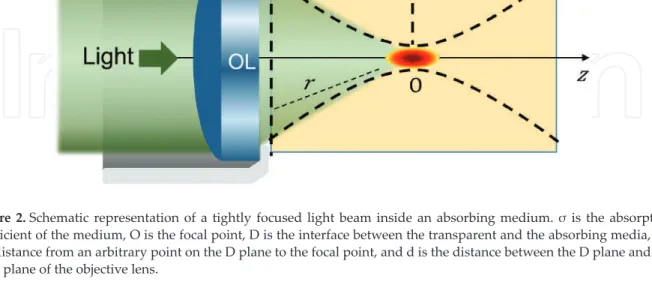
It is impossible to have an analytical solution of the light field at the focal point of a high NA OL. Red curve: normalization of intensity (If/I0) at the focal point as a function of the propagation length.

Verification of LOPA-based fabrication
In the case of LOPA, all these voxel shapes are obtained by simply adjusting the exposure time while keeping the laser power at a low value. Of course, the exposure time required to create sub-micrometer structures varies as a function of laser power.
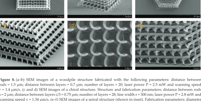
LOPA-based DLW for 3D microstructure fabrication
SEM measurements show that the bar line width on the top layer is about 320 nm, which is 1.5 times the standard voxel size. The physical causes of the distortion can be attributed to two main effects: the dose accumulation effect [22] and shrinkage effects [23].
Optimization of LOPA-based DLW technique
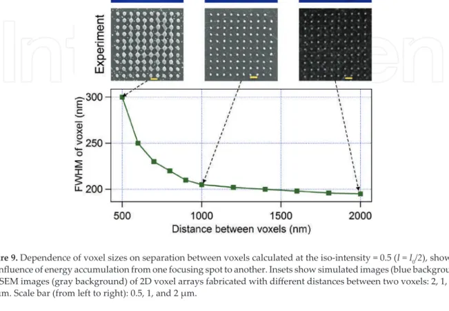
Dose accumulation effect
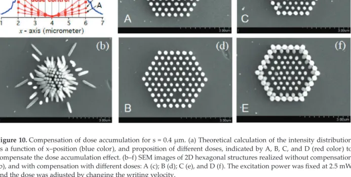
The intensity distribution of a pillar array and the dose compensation strategy are shown in Figure 10(a). The dose compensation technique is presented above and was shown to be able to compensate for the size difference in the structures.
Shrinkage effect
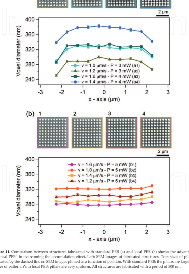
Due to the fact that the structures are not formed at low power (low light intensity), it is assumed that the applied laser power or intensity must be above a threshold to induce enough heat for the crosslinking process, and this threshold must be higher than that of standard LOPA (with PEB) for a complete photopolymerization. In contrast to the structures fabricated with traditional PEB, which show accumulation effect (Figure 11(a) at the top), the structures obtained with local PEB show almost perfect uniformity (Figure 11(b) at the top).
Realization of magneto-photonic microstructures by LOPA-based DLW
In conclusion, the multi-anchor supporting method was successfully applied to reduce the non-uniform deformation of 3D microstructure caused by adhesion to the substrate. The magnetic structures reacted strongly to the external magnetic field, which opened up many promising applications, such as tunable photonic structures based on magneto-optical effect and the development of microrobotic tools for transport in biological systems.
Conclusions and prospects
The whole process from structural development to the movement to a higher gradient of the external magnetic field was observed through an optical microscope, with all micropillars moving rapidly towards the magnetic tip, which confirmed the presence of Fe3O4 MNPs in the structures and their strong response to the applied magnetic field.
Author details
Controlled coupling of a single nanoparticle into a polymeric microstructure by direct laser writing technique with a low absorption of one photon. Single photon absorption based direct laser writing of three-dimensional photonic crystals http://dx.doi.org/10.5772/intechopen.71318 157.
TOP 1%
One-Photon Absorption-Based Direct Laser Writing of Three-Dimensional Photonic Crystals
Introduction
In Section 2, the theory of the LOPA-based DLW method and experimental conditions to realize 3D sub-microstructures are presented. In the last part, some conclusions of the newly developed LOPA-based DLW technique, advantages that this technology brings to the photonic crystal field, as well as some prospects will be discussed.
Theory of LOPA-based DLW technique
- Electromagnetic field distribution of a tight focused beam in an absorbing medium The mathematical representation of the electromagnetic field distribution in the focal region
- Numerical calculation of point spread function
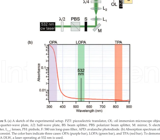
The light intensity distribution, also called the point spread function (PSF), in the focal region of the OL is defined as. The result of the numerical calculation, derived from the quadratic dependence of the EM field, is shown in Figure 3(a3). The size of the focus spot (full width at half maximum, FWHM) is quite large due to the use of a long wavelength.
In summary, to realize LOPA-based microscopy, two important conditions are required: (i) ultra-low absorption of the studied material at the chosen excitation wavelength and (ii) a high NA OL for tight focusing of the excitation light beam. . Dotted curves: zoom intensity profiles of the focus spot along the optical axis, calculated at different d.
Experimental demonstration of LOPA-based 3D microfabrication
- Experimental setup and fabrication procedure
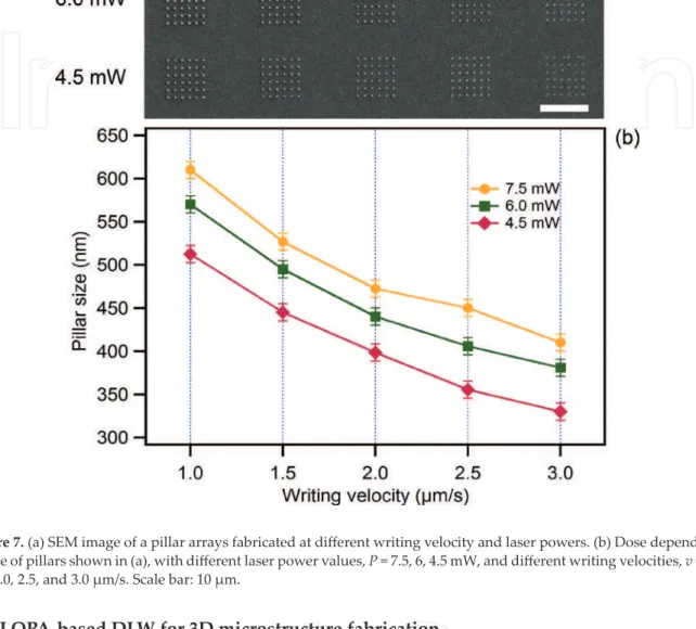
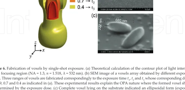
The dose dependence can be explained theoretically by calculating the iso-intensity of the focusing point at different levels. In the manufacturing process, the dose was adjusted by changing the speed of the PZT movement while the input power is fixed. It is noted that SU-8 exhibits a strong shrinkage effect, resulting in distortion of the fabricated structure.
The idea of the compensation technique is based on a balance of exposure doses over the structure. In other words, a certain amount of the exposure dose should be reduced in the region (or a part or a compartment) where the effect of dose accumulation is strongly manifested and should be increased in the region where the dose is absent. Dose accumulation compensation for s = 0.4 μm. a) Theoretical calculation of intensity distribution as a function of position x (blue color) and proposal of different doses, indicated by A, B, C and D (red color) to compensate the effect of dose accumulation.
-Direct laser writing of three-dimensional photonic crystals based on photon absorption (http://dx.doi.org/10.5772/intechopen only 8 mT) generated by a permanent magnet was then used to study the magnetic field response of magnetic micro-swimmers.
1D Photonic Crystals: Principles and Applications in Silicon Photonics
1D Photonic Crystals: Principles and Applications in Silicon Photonics
Fundamentals of 1D photonic crystals
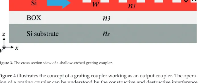
In silicon photonics, the 1D photonic crystals can be formed by periodic strip structures as shown in Figure 1. In this chapter we will focus on longitudinal periodic structures since longitudinal structures can be easily integrated with sub-micrometer. a) Top view and (b) cross section of a 1D photonic crystal. Nowadays, extensive review papers and books are available to fully understand the specific electromagnetic properties of the periodic structures considered here [16].
The equivalent effective index of the structure can be expressed with the zero-order approximation [17]: . where w/Λ is the duty cycle of the structure. So both effective index and effective birefringence can be designed by adjusting the geometry of the structure.
![Figure 2 shows a schematic k–ω diagram of a 1D periodic structure with lengthwise propaga- propaga-tion (along the x-axis) [16]](https://thumb-ap.123doks.com/thumbv2/1libvncom/9200670.0/58.918.138.778.807.1211/figure-schematic-diagram-periodic-structure-lengthwise-propaga-propaga.webp)
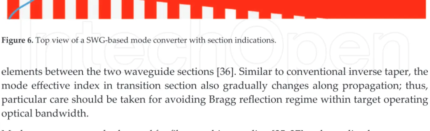
Applications of diffraction regime
The operation of a grating coupling can be understood by the constructive and destructive interference arising from the wavefronts generated by the diffraction of light from the grating stripes [18, 19]. The main reason is that the relatively short light extraction length between a fiber and a grating coupler generally causes a strong disturbance in the waveguide. Diagrams describing the concept of a grid link that acts as an output link. a) Vertical first order diffraction and backward second order diffraction and (b) tilted first order diffraction without second order diffraction.
When considering the grating coupler with SWG structures shown in Figure 5, the effective index of the TE (z-polarized) mode will be much larger than that of the TM (y-polarized) mode in the silicon wafer regions. A grating coupler with a bandwidth of ∼100 nm and a coupling efficiency of −5.6 dB was presented in Ref.
Applications of sub-wavelength regime
- Mode converters
- Waveguide crossings
- MMI couplers
- Polarization-independent directional couplers
In the sub-wavelength regions, from Eq. 1) and (2), the effective index of the TE mode n⊥ was found to be smaller than the TM mode n‖. Due to the high-index contrast of the silicon platform such as SOI, the insertion loss of a conventional waveguide junction is approximately 0.15 dB. The coefficients are determined by input mode profile and the structure of the central section (MMI section).
About reducing supported modes in the central section, reducing the width of the MMI section (same effect as that of using tapered inputs) and increasing lateral cladding index (reducing core cladding refractive index contrast) are feasible methods. 4), the beat length is described only for a certain wavelength. In results, the bandwidth of the MMI coupler in Figure 10b is determined by the pitch.
Applications of Bragg reflection regime
- Hybrid lasers with Bragg gratings
- TM-pass polarizers
By adjusting the duty cycle, if the effective indices of the TE mode n⊥ and TM mode n‖ in SWG structures meet the nkTE and nkTM for the same beat length for TE and TM modes, then the optimum duty cycle becomes reach. The basic rationale of designing a polarizer is to lose or filter unexpected polarization states from the optical propagation paths with a negligible effect on the desired polarization state and to keep the device size as small as possible. On the other hand, for TE polarization condition, the waveguide works as a Bragg reflector, and consequently the incident TE polarized light is reflected with very high efficiency.
Intrinsically, for a well-supported TE mode of a strip waveguide, the effective index of the TM mode is smaller than that of the TE mode, and therefore once Eq. Thus, the flow of the design process can be as follows: (1) use the Bragg reflection regime condition to roughly estimate the parameters of the photonic crystal; (2) simulate the k–ω plots for both TE and TM modes using 3D FDTD; and (3) calculate the transmission responses for both TE and TM modes to further verify the design.
Conclusion
High-efficiency fiber-on-chip network couplers realized using an advanced silicon-on-insulator CMOS compatible platform. Two-mode de/multiplexer based on multimodal interference coupler with a biased coupling as a phase shifter. DWDM Source Based on Laser Monolithic DFB Sidewall Sampling Network, in Conference on Lasers and Electro-Optics, OSA Technical Digest (2016) (Optic Society of America, 2016), paper SW4M.1.
Adhesive bonding of InP∕InGaAsP matrices to processed silicon wafers on an insulator using DVS-bis-benzocyclobutene. An integrated optical polarizer for silicon-on-insulator waveguides using evanescent wave coupling to gap plasmon polaritons.
Liquid Crystals for Responsible Photonic Crystals
Self-organized PCs and PBG tuning based on LCs
- Self-organized LC nanostructures
- PBG tuning of 3D photonic crystals
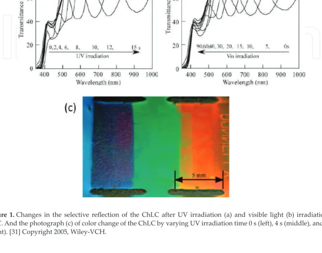
It is based on the photochemical change in helical twist power (HTP) of chiral azobenzene compounds under UV and visible light irradiation. Changes in the selective reflectance of ChLC after UV (a) and visible light (b) irradiation at 25°C. When the SiO2 inverse opal film was infiltrated with 4-cyano-4'-pentylbiphenyl (5CB), the reflectance spectra of the LC-infiltrated inverse opal film changed with increasing temperature as shown in Figure 3 .
It is due to the thermal back reaction of the azobenzene compound and the fluidity of the low molar mass LC. By irradiation with linearly polarized light at 488 nm (Ar + laser), azobenzene groups were aligned in the direction perpendicular to the polarization direction of the laser light.
Conclusion
Preparation of polymeric liquid crystal/cholesteric liquid crystal composites and their photochemical switching and memory properties by photoisomerization of a chiral azobenzene molecule. Tunable two-photon pumped lasing using a holographic polymer-dispersed liquid crystal lattice as a distributed feedback element. Lasering in photonic crystals based on dye-doped holographic polymer-dispersed liquid crystal reflection gratings.
Control of optical properties of liquid crystal infiltrated inverse opal structures using photo radiation and/or an electric field. Control of the optical band structure of liquid crystal infiltrated inverse opal by a photoinduced nematic-isotropic phase transition.
![Figure 9. Reflection spectra of Paz-infiltrated SiO 2 film with parallel and perpendicular LPL irradiation of Ar + laser and plot of the wavelength of reflection peak [59].](https://thumb-ap.123doks.com/thumbv2/1libvncom/9200670.0/89.918.136.785.247.604/figure-reflection-infiltrated-parallel-perpendicular-irradiation-wavelength-reflection.webp)