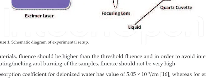
The presence of a dense medium adjacent to the molten layer of the target causes various instabilities. The initial reduction in peak intensity is due to the recrystallization of the irradiated targets during resolidification after melting.
![Figure 1 shows the schematic diagram of the experimental setup. Threshold fluence for Zr was calculated by using following relation [15].](https://thumb-ap.123doks.com/thumbv2/1libvncom/9201724.0/4.918.105.809.976.1166/figure-schematic-diagram-experimental-threshold-calculated-following-relation.webp)
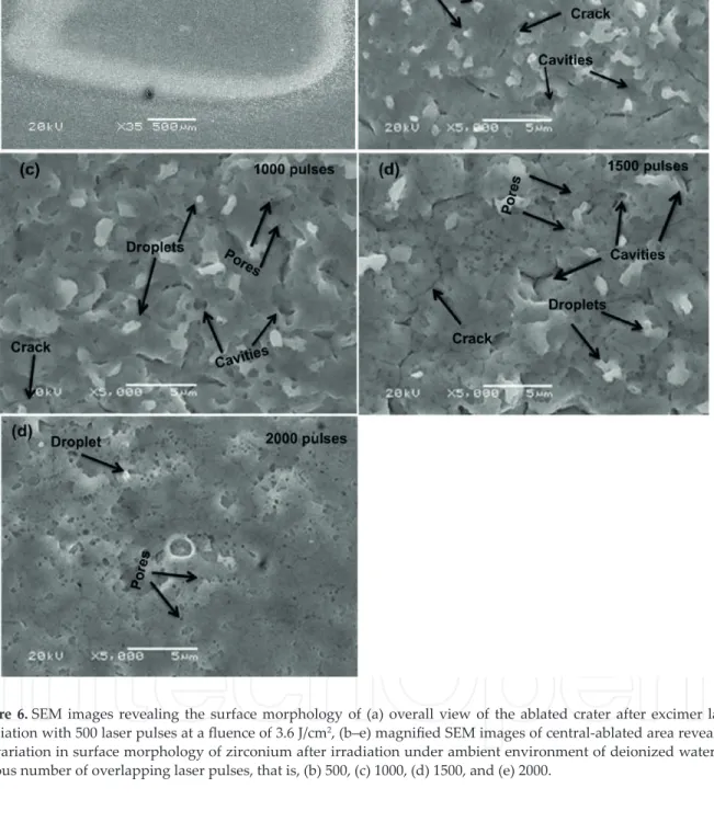
Effect on surface morphology
The plasma-induced pressure will lead to a further temperature increase of the laser-induced plasma. Furthermore, the cooling effect of the liquids causes quenching of the plasma plume and the plume species will be redeposited over the target surface.
Effect on surface mechanical property
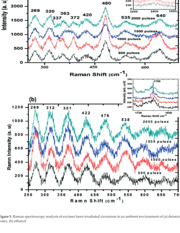
This results in the formation of voids, pores, cracks and droplets over the surface after irradiation. Increase in hardness is due to interstitial diffusion of oxygen in the lattice, resulting in a decrease in crystallite size and tensile residual stresses (Figure 3b) [40].
Conclusion
The smaller crystallite size is efficient in inhibiting dislocation motion and is responsible for high strength and toughness. The decrease in the hardness value of the irradiated targets can be explained on the basis of the increase in the crystallite size and the increase in the residual tensile stresses.
Author details
Effect of flux and surrounding environment on the surface and structural modification of femtosecond laser irradiated Ti. Pressure generation and measurement in rapid evaporation of water on a pulsed laser-heated surface.
Sequentially Timed All-Optical Mapping Photography for Real-Time Monitoring of Laser Ablation
Breakdown and Filamentation in Picosecond and Femtosecond Regimes
- Introduction
- High-speed imaging techniques for monitoring fast process of ultrashort laser ablation
- Conventional techniques for capturing ablation dynamics
- Sequentially timed all-optical mapping photography for sub-nanosecond single-shot imaging
- Real-time observation of early stage plasma evolution during femtosecond laser ablation
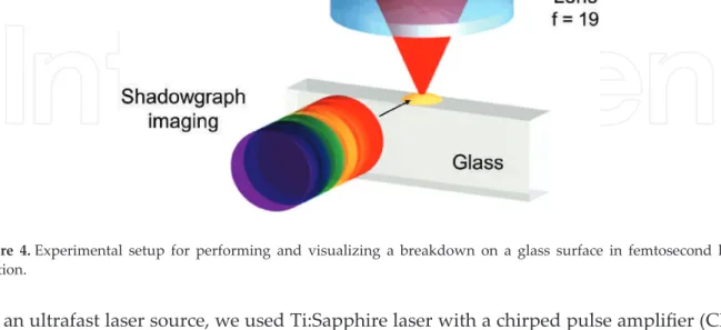
- Experimental setup of ultrashort laser ablation and STAMP with spectral shaper As shown in Figure 4, the surface of a glass plate was ablated by a focused femtosecond laser
- Plasma generation and expansion around glass surface
- Real-time monitoring of plasma filament generated by femtosecond laser inside a glass
- Experimental setup of filamentation and STAMP with spectral filtering
- Femto-to-picosecond dynamics of plasma filaments inside a glass
- Conclusion
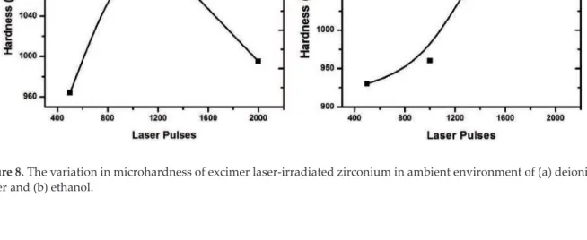
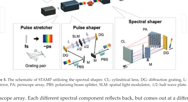
All these direct approaches must face limitations in the response speed of the device or material. The daughter pulses encoded by the image are "passively" and "optically" separated by the spatial mapping device and occur in different areas of the image sensor. The data recorded on the image sensor is digitally processed on the computer to reconstruct the movies with the frame interval and exposure time calibrated by the pulse stretcher and pulse shaper settings in the temporal mapping device.
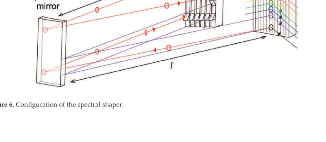
It can be tuned depending on the time scale of the dynamic event of interest [13]. In the spectral former, a periscope array is placed in the Fourier plane in the 4f configuration of the spectral former (Figure 6). These daughter pulses were detected at the different position of the high-sensitivity image sensor pixels).
Figures 12 and 13 are motion pictures of dynamic events in femtosecond laser ablation. As a result, time-varying target profiles were mapped to different positions of the image sensor.
Acknowledgements
In this chapter, we introduced the STAMP movie camera and presented movies of femtosecond laser ablation. The principle of this imaging method is based on the all-optical image of time-varying spatial profiles of the target. We introduced two examples of the STAMP configurations: STAMP uses the spectral shaper and uses the spectral filtering and spectral broadening.
Using STAMP, we obtained sequential images of sub-nanosecond dynamic events under the process of femtosecond laser ablation. Laser breakdown induced by intense femtosecond laser pulse was monitored with a frame interval of 15.3 ps and a total of six frames. As demonstrated in this chapter, STAMP is a useful tool to understand precise processes of complex dynamics in ultrashort laser ablation.
Coulomb explosion and early plasma generation during femtosecond laser ablation of silicon at high laser fluence. Single-frame measurement of the complete spatiotemporal intensity and phase of ultrashort laser pulses using wavelength-multiplexed digital holography.
Optical Properties of Complex Oxide Thin Films Obtained by Pulsed Laser Deposition
Ellipsometry
In 1902, Paul Drude published the chapter "Polarisation" in the book "The Theory of Optics", which still serves as a modern introduction to the study of polarized light and ellipsometry [7]. The complex refractive index is composed of a real part "n" and an imaginary part "k". The imaginary part is called the extinction coefficient and is directly related to absorption of the light in the material. In the case of thin film systems, the purpose of ellipsometry measurement is to determine the optical properties of the materials based on the measured Ψ and Δ parameters.
In the optical model, some parameters are unknown, such as the thickness or the values of optical constants. After obtaining the best fit and the minimum MSE value, the values of the optical constants can be generated. The values of the refractive index, the extinction coefficients and the thickness of the thin film are considered as unknown parameters.
The optical model will also usually include a clear top layer, which is responsible for the roughness of the thin film. Once the unknown parameters of thin film are determined, the value of thickness and dielectric function of the rough top layer will be calculated.
Results and discussion
Usually, the experimental data of ΨenΔ were obtained in the 250–1700 nm range of wavelengths, with a step of 2 nm. From Figure 7, it is easy to observe the difference in the optical behavior for YBCO thin film growth in different conditions. In the case of RF-PLD thin film growth at lower temperature (730C) but in the presence of oxygen RF discharge (without post-annealing treatments), the value of refractive index and extinction coefficients are higher, and the optical behavior varies in the range of 250 –600 p.m.
The difference in the optical behavior can be explained by this difference in an oxidized state of the YBCO layer. In both cases, the dielectric function of the substrates was taken from the literature and the rough top layer was estimated to be 50% air and 50% SBN in the Bruggeman approach. The film thickness and roughness were obtained by fitting the experimental data with a Cauchy dispersion model in the range of 1.2–2 eV (620–1030 nm).
The experimental data of Ψ and Δ were obtained in the wavelength range of 250-1700 nm with a step of 2 nm. As in the case of SBN, the mounting procedure consists of two steps: first, the thicknesses of thin films and the roughness were calculated based on the fitting of the experimental data in the 600–1700 nm range.
Conclusions
The results of XRD indicate polycrystalline randomly oriented thin films of BNT-BT growth by PLD on Pt/Si substrate [40]. For ferroelectric materials, the Tauc-Lorentz [43] or Cody-Lorentz oscillators are more flexible at higher energies in the ultraviolet range of the spectrum. Infrared and Raman spectroscopic studies of optically transparent zirconia (ZrO2) films deposited by plasma-assisted reactive pulsed laser deposition.
31] Stanciu G, Scarisoreanu ND, Ion V, Moldovan A, Andronescu E, Dinescu M. Ba2Cu3O7-δ thin films deposited by pulsed laser deposition and radiofrequency-assisted pulsed laser deposition. Laser Ablation - From Fundamentals to Applications 142. 35] Ion V, Galca AC, Scarisoreanu ND, Filipescu M, Dinescu M. Spectroscopic ellipsometric study of amorphous SrxBa1xNb2O6 thin films obtained by pulsed laser deposition. Structural, optical and electrical properties of BNT-BT0.08 thin films processed by sol-gel technique.
Optical properties of lead-free Na0.5Bi0.5TiO3 epitaxial piezoelectric thin films: ellipsometric and theoretical studies. Structural and electrical characterization of lead-free ferroelectric Na1/2Bi1/2TiO3–BaTiO3 thin films obtained by PLD and RF-PLD.
Nanoparticles, Nanocrystals, and Nanocomposites Produced with Pulsed Laser Ablation and Their
Laser-material interaction and pulsed laser ablation in liquid method
When the laser energy is delivered to the material surface, three main cases - reflection, transmission and absorption - play a significant role in the results of the interaction. In the first two cases, after the laser beam hits the material, some of the incoming laser energy is reflected due to the real part of the refractive index and the rest of the laser energy is transmitted through the material. The reflection of the material also depends on the frequency (or wavelength) of the light source.
In the third case, some of the laser energy is absorbed by the material due to its absorption coefficient (α), and the laser intensity decreases exponentially as it moves inside the material. For example, some of the materials have strong non-linear properties, which affect the refractive index variation for different wavelengths; thus the whole process will be affected and changed such as self-focusing, defocusing and soliton propagation [3]. When the material directly absorbs the laser energy, the removal of the material is observed.
Ablation of materials occurs when the laser energy becomes greater than the fluence threshold. Material properties such as absorption, material defects, and general material properties are also important for ablation.
Outline of book chapter
Nanoparticles, nanocrystals, and nanocomposites from pulsed laser ablation
- Metal nanoparticle generation
- Semi-conductor nanoparticle generation
- Other types of nanoparticles produced by PLAL 1. Generation of nanoparticles from biological samples
In Figure 1b, the resistance response of the Au-NP films when the strain is applied is presented. The high sensitivity of Au-NPs generated by the PLAL method used in strain sensors is related to the non-contaminated NP surfaces, to the size of the NPs. In both studies, Ag-NPs were produced in water using a commercial nanosecond pulsed ND:YLF laser (Empower Q-Switched Laser, Spectra Physics) (wavelength 527 nm, pulse duration 100 ns, average output 16 -W power, 1-kHz pulse repetition rate, and 16-mJ pulse energy).
The distribution and toxicity of the pure Ag-NPs produced by PLAL in the rat hippocampal slices were determined. Result of the XRD analysis of GaN-NPs (product) produced by PLAL with a femtosecond laser in ethanol and the starting material GaN powder (educt). Moreover, the nanoparticle size at the end of PLAL depends on the initial size of the suspended particles [52, 53].
XRD analysis shows that the MoS2 nanosheets have a hexagonal crystal structure. a) Schematic of MoS2 nanocrystals with different shapes in different liquids and (b) optical microscope image of generated MoS2 nanocrystals [54]. At the same time, the chemical method of producing silica nanoparticles was used for the comparison of the final products.
![Figure 1. (a) Au-NP film-deposited strain sensors, (b) resistive response of the Au-NP film [9].](https://thumb-ap.123doks.com/thumbv2/1libvncom/9201724.0/65.918.112.808.245.522/figure-film-deposited-strain-sensors-resistive-response-film.webp)
Applications
- Thin film MoS 2 nanocrystal-based ultraviolet photodetector
- A plasmonic-enhanced photodetector based on silicon nanocrystals obtained through laser ablation
- A near-infrared range photodetector based on indium nitride nanocrystals obtained through laser ablation
- Enhancement in c-Si solar cells using 16-nm InN nanoparticles
- Enhanced memory effect via quantum confinement in 16-nm InN nanoparticles embedded in ZnO charge-trapping layer
- Biological applications
A near-infrared photodetector based on indium nitride nanocrystals obtained by laser ablation. Synthesis of gold nanoparticles by laser ablation of Au foil inside and outside ionic liquids. Post-processing of silicon nanocrystals produced by ultrashort pulse laser ablation in liquid: towards the creation of blue luminescent nanocrystals.
In situ bioconjugation: A one-step approach to tailored nanoparticle bioconjugates by ultrashort pulse laser ablation. Synthesis of blue-shifted luminescent colloidal GaN nanocrystals by femtosecond pulsed laser ablation in organic solution. Generation of InN nanocrystals in organic solution by laser ablation of InN thin film grown by high-pressure chemical vapor deposition.
Generation of ultrasmall InN nanocrystals by pulsed laser ablation of suspension in organic solution. Novel one-step synthesis of silica nanoparticles from sugar beet bagasse by laser ablation and its effects on the growth of freshwater algal culture.
![Figure 9. (a) SEM image of Ag-NCs; inset: size distribution of them, (b) schematic representation of the photodetector, (c) UV–vis absorption of Ag-NCs on quartz, (d) photo-generated current versus wavelength spectrum [71].](https://thumb-ap.123doks.com/thumbv2/1libvncom/9201724.0/75.918.114.810.243.642/distribution-schematic-representation-photodetector-absorption-generated-wavelength-spectrum.webp)
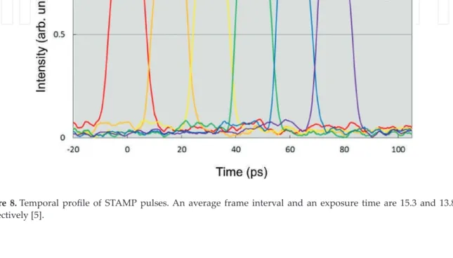
![Figure 8. Temporal profile of STAMP pulses. An average frame interval and an exposure time are 15.3 and 13.8 ps, respectively [5].](https://thumb-ap.123doks.com/thumbv2/1libvncom/9201724.0/31.918.143.775.533.779/figure-temporal-profile-stamp-average-interval-exposure-respectively.webp)
