Research Journal of Applied Sciences, Engineering and Technology 7(13): 2701-2704, 2014 ISSN: 2040-7459; e-ISSN: 2040-7467
© Maxwell Scientific Organization, 2014
Submitted: August 27, 2013 Accepted: September 07, 2013 Published: April 05, 2014
Corresponding Author: M. Idzdihar Idris, Faculty of Electronic and Computer Engineering, Universiti Teknikal Malaysia Melaka, Hang Tuah Jaya, 76100 Durian Tunggal, Melaka, Malaysia
2701
Deposition of Micro Contact Based Probe Cell for IC Testing by Dc Magnetron
Sputtering Technique
1, 2M. Idzdihar Idris, 2Nowshad Amin, 1Faiz Arith and 2S.A.M. Chachuli
1Faculty of Electronic and Computer Engineering, Universiti Teknikal Malaysia Melaka,
Hang Tuah Jaya, 76100 Durian Tunggal, Melaka, Malaysia
2Solar Energy Research Institute, Universiti Kebangsaan Malaysia, UKM, Bangi 43600,
Selangor, Malaysia
Abstract: This study presents the deposition of micro contact probe cell for IC testing deposited by dc sputtering technique on a glass substrate. Micro contact with thickness of 2800-7000 nm were deposited from Copper target at sputtering power of 125 W in argon ambient at a room temperature on a base layer of copper using mask. Then, the micro contacts were investigated by using profilometer. All the obtained results show the potential viability of the novel test fixture and thus solve the limitation of the pogo pin based testing tools by replacing them with the novel IC test fixture as demonstrated in this study.
Keywords: DC sputtering deposition, micro contact, pogo pin, test socket
INTRODUCTION
Integrated circuits are tested in final step of IC packaging to verify that required electrical connections are working properly. Different devices are used in this step such as Automatic Test Equipment (ATE), test handler, load board, test socket and etc. Pogo pin based test socket has been adapted well in performing the final testing of Integrated Circuit (IC) in semiconductor industries (Amit and Sivakumar, 2005). However, the conventional pogo pin has several limitations and brings several kinds of problem to new fine pitch IC packages such as puncture marks which cause to decrease the yield of manufacturing process (Amin and Lam, 2008; Teng et al., 2007). Designing a new method as the replacement of pogo pin is unavoidable. Therefore, it is necessary to determine an appropriate new contact mechanism in order to overcome the problem. A novel electrical contact mechanism has been proposed by utilizing a combination of three different kinds of materials such as polymer, metallic and liquid metal (Lam et al., 2009). In previous study, the new model of test socket with new materials in different shapes were designed by using ANSYS as Finite Element Analysis (FEA) software and the best parameters were obtained (Ehtiatkha et al., 2011). Test socket is formed as an array of holes and is filled with electrical conductive cells where the cells can be inserted according to IC lead counts and size. In this study, according to optimized parameter obtained from previous simulation result, prototype structures of the
micro-contacts are deposited by using DC Sputtering with copper as a material on glass substrate. In addition, the thickness of the micro contact was also investigated in this study.
MATERIALS AND METHODS
Micro contact sputter parameter: Table 1 shows the sputter deposition parameters for micro contact. The built-in thickness-monitoring module (quartz crystal thickness monitor) monitors the thickness of the deposited material. The sputter deposition system will stop depositing when the desired thickness is achieved. The vacuum chamber is being vacuumed to the base pressure in the order of 10-15×10-3 Torr by running the turbo-molecular pump. In this experiment, all the sputter deposition samples were ran under DC power of 150 Watt and the substrates initial and final temperature were recorded. However, the substrate final temperature increased without being heated by the substrate holder. This is mainly due to the heat transfers from the magnetron gun and the plasma to the substrate. Four set Table 1: Parameters for the micro-contact sputtering deposition
Res. J. App. Sci. Eng. Technol., 7(13): 2701-2704, 2014
2702
Fig. 1: Deposition of copper base
Fig. 2: Deposition of the micro-contact columns: deposition mask covered the substrate with copper base
Fig. 3: Deposition of the micro-contact columns: deposition mask is removed carefully after the micro-contact columns were formed
of samples were deposited with different deposition time (A1, A2, A3 and A4).
Deposition of micro contact: The fabrication of the micro-contact metallic layer is divided into two main steps. The first step is to deposit the metallic base. This metallic base is the ground where the micro-contact columns will be grown. After the metallic base is sputter deposited as shown in Fig. 1, the square metallic base is then exposed and ready for the next step.
After that, the mask with circular openings covers the substrate with metallic base and the sputter deposition process was performed again on the substrate as shown in Fig. 2. The copper materials deposited into the openings of the mask forms the pattern of the micro contact columns as shown in Fig. 3 after the deposition mask was carefully removed. Finally, the deposition mask will be cleaned with a liquid consist of 50% of HCI and 50% of deionizer water so that it can be used to fabricate other samples. It is important to note that the surrounding micro contact has a thicker layer of copper compare to the base layer. Therefore, the sample must be cut to see the cross section of the micro contact. In the future of bringing this concept for mass production, mask alignment instruments can be introduced into the fabrication process if more resources are available.
RESULTS AND DISCUSSION
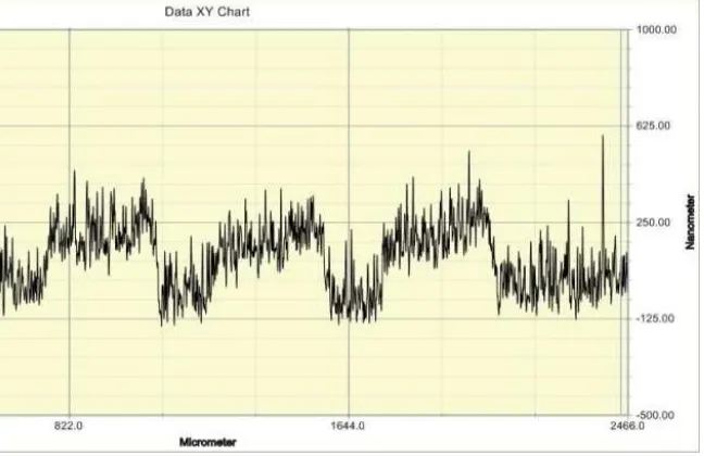
Profilometer: The profilometer is used to determine the thickness of the micro contact column on the base copper layer. During the sputter deposition, the material deposited is being monitored by quartz crystal thickness monitor. However, the thickness of material that deposits on the crystal is not necessarily the same as what has been deposited on the sample.
The results of the Dektak profilometer for sample A1, A2, A3 and A4 are shown in Fig. 4 respectively. The results show that the deposited micro-contact columns form a column shape structure, which is desired and ideal for oxidation layer penetration. The micro contact thickness not increases linearly with deposition time. Sample A3 has the highest micro
Res. J. App. Sci. Eng. Technol., 7(13): 2701-2704, 2014
2703
Sample A2
Sample A3
Sample A4
Res. J. App. Sci. Eng. Technol., 7(13): 2701-2704, 2014
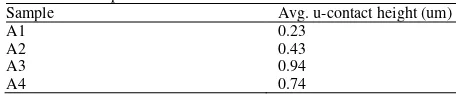
2704 Table 2: The measured thickness of micro contact column from
dektak profilometer
Sample Avg. u-contact height (um)
A1 0.23
A2 0.43
A3 0.94
A4 0.74
Avg.: Average
contact columns rather than sample A4 even the deposition time is shorter. This may happen due to the shadow effect that increasing the diameter of micro contact column instead of micro contact height. The thickness of the micro-contact columns on different samples are indicated in Table 2.
CONCLUSION
Deposition of the micro contact by DC magnetron sputtering technique and its analysis has been presented in this study. Dektak thickness profilometer showed that the micro-contact columns were formed with the desired column shape which is ideal for oxidation layer penetration and the highest micro contact thickness achieved was 0.94 um. Theoretically, the micro contact height or thickness increase linearly with the deposition time. However, there is a factor like shadow effect that has give some influence to the thickness of micro contact thickness. Because of the shadow effect, the micro contact diameter becomes wider instead of thicker. This point should be taken for consideration in order to fabricate the micro contact.
ACKNOWLEDGMENT
The authors would like to thank to Universiti Kebangsaan Malaysia (UKM), University Technical
Malaysia Melaka (UTeM) and Ministry of Higher Education for the support, facilities and financial support throughout the project.
REFERENCES
Amin, N. and Z.Y. Lam, 2008. A practical investigation on the root causes of the mechanical damages of pogo pin type test sockets to IC packages in final test. Proceeding of IEEE International Conference on Semiconductor Electronics (ICSE 2008), pp: 393-397.
Amit, K.G. and A. Sivakumar, 2005. Single machine scheduling with multiple objectives in semiconductor manufacturing. Int. J. Adv. Manuf. Tech., 26: 950-958.
Ehtiatkha, Z., S. Basiri and N. Amin, 2011. Mechanical design and analysis of innovative integrated circuit test socket. Proceeding of IEEE Regional Symposium on Micro and Nan Electronics (RSM), pp: 65-69.
Lam, Z.Y., H.W. Koay and N. Amin, 2009. Semiconductor final test fixture design with microstructure alloy contacts using finite element analysis. Proceeding of 11th Electronics Packaging Technology Conference (EPTC '09), pp: 834-837. Teng, H.C., M.K. Chen, C.H. Yeh, Y.J. Huang and