i
DESIGN POWER AMPLIFIER FOR GPS APPLICATION
SURIANI BINTI MD NAYAN
This Report is Submitted in Partial Fulfillment of Requirements for the Bachelor Degree of Electronic Engineering (Telecommunication Electronics)
Faculty of Electronic and Computer Engineering Universiti Teknikal Malaysia Melaka
ii
UNIVERSTI TEKNIKAL MALAYSIA MELAKA
FAKULTI KEJURUTERAAN ELEKTRONIK DAN KEJURUTERAAN KOMPUTER
BORANG PENGESAHAN STATUS LAPORAN
PROJEK SARJANA MUDA II
Tajuk Projek : DESIGN POWER AMPLIFIER FOR GPS APPLICATION BASE ON S-PARAMETER
Sesi
Pengajian : 1 0 / 1 1
Saya SURIANI BINTI MD NAYAN
mengaku membenarkan Laporan Projek Sarjana Muda ini disimpan di Perpustakaan dengan syarat-syarat kegunaan seperti berikut:
1. Laporan adalah hakmilik Universiti Teknikal Malaysia Melaka.
2. Perpustakaan dibenarkan membuat salinan untuk tujuan pengajian sahaja.
3. Perpustakaan dibenarkan membuat salinan laporan ini sebagai bahan pertukaran antara institusi
pengajian tinggi.
4. Sila tandakan ( √ ) :
SULIT*
*(Mengandungi maklumat yang berdarjah keselamatan atau kepentingan Malaysia seperti yang termaktub di dalam AKTA RAHSIA RASMI 1972)
TERHAD** **(Mengandungi maklumat terhad yang telah ditentukan oleh
organisasi/badan di mana penyelidikan dijalankan)
TIDAK TERHAD
Disahkan oleh:
__________________________ ___________________________________
(TANDATANGAN PENULIS) (COP DAN TANDATANGAN PENYELIA)
iii
“I hereby declare that this report is the result of my own work except for quotes as cited in the references “
Signature :………
Author : SURIANI BINTI MD NAYAN
iv
“I hereby declare that I have read this report and in my opinion this report is sufficient in terms of the scope and quality for the award of Bachelor of Electronic
Engineering ( Telecommunication Electronics) with Honours.”
Signature :………
Supervisor Name :
Date : 21APRIL 2011
v
ACKNOWLEDGEMENT
I wish to express sincere, heartfelt appreciation to those involved in the completion of this project.
First and foremost, I wish to express special thanks, appreciation and deep gratitude t my project supervisor, Encik Azahari bin Salleh, who has been there to provide continuous guidance, advice, encouragement, support and generous amount of time in helping me to complete this project. His remarkable unique ways and professionalism of handling my weaknesses has turned my simplistic mind to see think in more rational and critical view. It has been a great pleasure and privilege tp learn from someone who is professional like him.
Sincere appreciation of course goes to my friends who give me unselfish support and special thanks to my parents, Md Nayan bin Md Isa and my mother Zauyah binti Mat Isa because always support me.
vi
ABSTRACT
vii
ABSTRAK
viii
CONTENTS
CHAPTER TOPIC PAGES
I INTRODUCTION
1.1 Project Background 1
1.2 Objective 2
1.3 Problem Statement 2
1.4 Project Scope 3
1.5 Thesis Outline 3
II GLOBAL POSITIONING SYSTEM
2.1 Global Positioning System (GPS) 5
2.2 GPS Orbits 6
2.3 GPS Signals 6
2.4 L1 Carrier Frequency 7
2.5 Demodulation and Decoding 8
2.6 Application of GPS 10
2.6.1 Roads and highway 10
2.6.2 Space 12
2.6.3 Rails 13
2.6.4 Aviation 14
2.6.5 Marine 15
ix
III AMPLIFIER DESIGN
3.1 Power Amplifier 17
3.1.1 Efficiency 18
3.1.2 Power Gain/ Voltage Gain 18
3.1.3 Linearity 19
3.1.4 1-dB compression 19
3.1.5 Power Consumption 20
3.1.6 Noise Figure 20
3.2 Class of Amplifier 20
3.2.1 Class A operations 21
3.3 Single Stage Amplifier 22
3.4 Scattering Parameters 23
3.5 Two-port Scattering Parameters 24 3.6 Relationship with voltage and current 25
3.7 Meanings of s-parameters 25
3.8 Gain Definitions in Power Amplifier 26 3.9 Transducer Power Gain of Two-Port Circuit 27
3.10 Stability of Amplifier 29
3.10.1 Conditions for Stability 29
3.11 DC Biasing 31
IV PROJECT METHODOLOGY
4.1 Project Expectation Work Flow 33
4.2 Stability 35
4.3 Matching 36
4 .3.1 Lumped Element 38
4.3.2 Single Stub Element 40
x
V RESULT AND DISCUSSION
5.1 Selection of transistor 47
5.2 Calculation 49
5.3 Stability Consideration 54
5.4 IV Curve 55
5.5 DC Biasing Simulation Result 56
5.6 Matching Simulation Result 57
5.7 Type of input and output matching 57 5.7.1 Single Stub Matching Network 57 5.7.2 Quarter Wave Matching Network 58 5.7.3 Lumped Element Matching Network 58
5.8 S-Parameter Results 59
5.8.1 S21 Output Graft 59
5.8.2 Input Return Loss 60
5.8.3 Output Return Loss 62
5.8.4 Insertion Loss 63
5.8.5 Available Gain 64
5.8.6 Maximum Available Gain 65
5.8.7 Maximum Stable Gain 66
5.8.8 Power Gain 66
5.8.9 Transducer Gain 67
5.8.10 Current Gain 68
5.8.11 Noise Figure 71
5.9 Discussion 72
VI CONCLUSION AND RECOMMENDATION
6.1 Conclusion 73
xi
LIST OF FIGURES
FIGURE TITLE PAGES
Figure 1.1 Power Amplifier on GPS System 2
Figure 2.1 NAVSTAR GPS System Segments 6
Figure 2.2 GPS Signal Code and Carrier Frequency 7
Figure 2.3 GPS Satellite Transmission 8
Figure 2.4 Satellite Signals 9
Figure 2.5 Road and Highway 11
Figure 2.6 Space Application 12
Figure 2.7 Rail Application 13
Figure 2.8 Aviation Application 14
Figure 2.9 Marine Application 15
Figure 2.10 Agriculture Application 15
Figure 2.11 1-dB Compression Characteristics 18 Figure 2.13 General Transistor Amplifier Circuit 22
Figure 3.1 Project Expectation Work Flow 24
Figure 3.2 General Flow Chart of Designing GPS PA 26
Figure 3.3 Termination Matching Network 28
Figure 3.4 Waveguide Matching Network 28
Figure 3.5 Lumped Element Matching Network 30
Figure 3.6 Single Stub Matching Network 30
Figure 3.7 Quarter Wave Element 31
Figure 4.1 Scattering Parameter 34
Figure 4.2 Two-Port Scattering Parameters 35
xii
Figure 4.4 Transducer Power Gain using Z-parameters 37 Figure 4.5 Transducer Power Gain using S-parameters 38
Figure 4.6 Conditions for Stability 39
Figure 4.7 Unconditional Stability 40
Figure 4.8 Conditional Stability 40
Figure 5.1 Parameter define using AWR Software 43 Figure 5.2 S-Paramater define at frequency 1.575 MHz 43
Figure 5.3 Graft of Stability 44
Figure 5.4 Biasing Setup 45
Figure 5.5 IV Curve 45
Figure 5.6 DC Biasing 46
Figure 5.7 Single Stub Matching Network 47
Figure 5.8 Quarter Wave Matching Network 47
Figure 5.9 Lumped Element Matching Network 48
Figure 5.10 S21 Output Graft 49
Figure 5.11 S21 Output Optimization 49
Figure 5.12 Return Loss Input 50
Figure 5.13 Comparison Return Loss Input 51
Figure 5.14 Return Loss Output 51
Figure 5.15 Comparison Return Loss Output 52
Figure 5.16 Insertion Loss 53
Figure 5.17 Comparison Insertion Loss 53
Figure 5.18 Available Gain 54
Figure 5.19 Available Gain after Optimization 54
Figure 5.20 Maximum Available Gain 55
Figure 5.21 Maximum Available Gain after Optimization 55
Figure 5.22 Maximum Stable Gain 56
Figure 5.23 Operating Power Gain 56
Figure 5.24 Operating Power Gain after Optimization 57
Figure 5.25 Transducer Gain 57
xiii
Figure 5.27 Current Gain at S21 58
Figure 5.28 Current Gain 59
Figure 5.29 Current Gain 59
Figure 5.30 Comparison Voltage Gain VTG 60
Figure 5.31 Voltage Gain VTG 60
Figure 5.32 Comparison Noise Figure 61
xiv
LIST OF TABLE
TABLE TITLE PAGES
Table 1.1 Parameters Requirement 4
xv
LIST OF APPENDIXS
APPENDIX PAGES
APPENDIX A 77
APPENDIX B 80
APPENDIX C 81
APPENDIX D 82
CHAPTER I
INTRODUCTION
This chapter will discuss the overview process that involved for this project;
the aims and specific objectives of the project, problem statements, work scope,
methodology and result. The end of this chapter the thesis outline will be listed.
1.1 Project Background
This project implements the Power Amplifier (PA) for Global Positioning
System (GPS) system. It’s a software project but lastly must fabricate the result of
simulation. Power amplifier is building in satellite transponder on GPS transmission
system. Input signal is generally small and needs to be amplified sufficiently to
operate an output device. Power Amplifier is design to amplify that signal (RF
signal) and provides a large version of the signal that may direct to and antenna. It’s
also required to amplify the wanted signal without distortions and without other
impairments which would decrease the usefulness of the signal. Power Amplifier is
design operating in Class A linear mode over range of 1575.42 MHz. In this project,
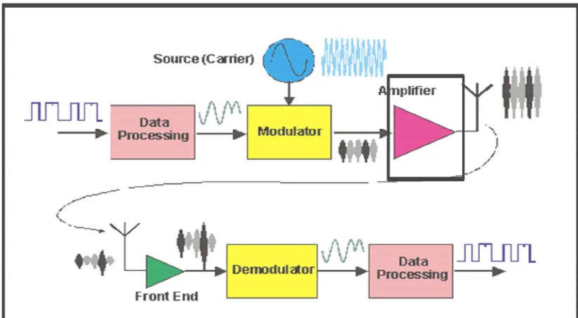
the transistor was use is the power transistor. Figure 1.1 shows the Power Amplifier
2
Figure 1.1: Power Amplifier on GPS system
1.2 Objective
Objective of this project is to design,, simulate and analysis the Power
Amplifier for GPS application. Design and analyze matching network base on
s-parameters for Power Amplifier at L1 Frequency (1575.42 MHz). The power
amplifier designed at L1 frequency (1575.42 MHz) for civilian.
1.3 Problem Statement
The amplifier is used to increase the signal that drives the signal to the
antenna. Without the amplifier, low-power radio-frequency cannot be converting into
a large signal of significant power. It’s also can’t optimized to have a high efficiency,
high output power compression, good return loss on the input and output, good gain
and optimum heat dissipation for driving a signal to the antenna. Signal also has a
3
1.4 Project Scope
Scope for this project is analyzing the power amplifier for GPS system at L1
frequency. The frequency is 1575.42MHz. The software that will be use is AWR to
simulate the power amplifier. Analyze the power amplifier base on stability, gain,
input and output return loss at frequency 1.575 GHz using AWR software. Analyze
and comparison on type of matching network base on this element:-
(a) Stub element
(b) Quarter wave element
(c) Lumped element
Table 1.1 shows the parameters that been used in this project:-
Table 1. 1 Parameters requirement
Parameter Requirement
Operating frequency 1.575 GHz
Gain >10dB
Bias Point VVE=2.7V
IC=10mA
Transistor AT-41533
1.5 Thesis Outline
Chapter 1 is about an introduction of project which includes an explanation of
project background, a brief introduction of Global Positioning System (GPS) and
Power Amplifier (PA), method used in Power Amplifier design, objectives of project,
and project scopes.
Chapter 2 of background study defines in detail about GPS and PA , and also
4
Chapter 3 contains a research methodology which includes the steps to design
power amplifier and a brief explanation of methodology flow chart.
Chapter 4 contains a details explanation of an amplifier design technique
which consist a single stage amplifier design, DC biasing design and input output
matching design.
Chapter 5 discusses about the selection of transistor and the result from this
project, S-parameter analysis, comparison matching network and all gain analysis.
Also include the calculation for design.
Chapter 6 reveals the conclusion of this project and future works suggestion
5
CHAPTER II
GLOBAL POSITIONING SYSTEM
2.1 Global Positioning System (GPS)
The GPS system consists of three pieces. There are the satellites that transmit
the position information, there are the ground stations that are used to control the
satellites and update the information, and finally there is the receiver that we
purchased. It is the receiver that collects data from the satellites and computes its
location anywhere in the world based on information it gets from the satellites GPS
is part of a satellite-based navigation system developed by the U.S. Department of
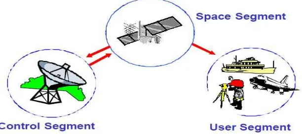
Defense under its NAVSTAR satellite program. Figure 2.1 shows the NAVSTAR
GPS System Segments.
6
2.2 GPS Orbits
The fully operational GPS includes 24 or more active satellites approximately
uniformly dispersed around six circular orbits with four or more satellite each. The
orbits are inclined at an angle of 55o relative to the equator and are separated from
each other by multiples of 60o right ascension. The orbits are no geostationary and
approximately circular, with radii of 26,560km and orbital periods of one half
sidereal days. Theoretically, there are more GPS satellite will always be visible from
most points on the earth’s surface and four or more GPS satellite can be used to
determine an observer’s position anywhere on the earth’s surface 24 hour per day.
2.3 GPS signals
Each GPS satellite carries a cesium and/or rubidium atomic clock to provide
timing information for the signals transmitted by the satellites. Internal clock
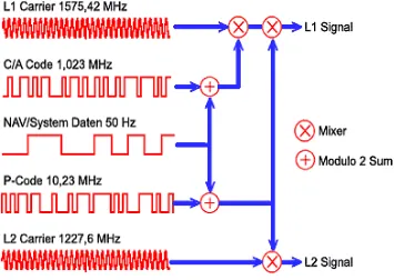
correction is provided for each satellite clock. Each GPS satellite transmits two
spread spectrum, L-band carrier signal. L1 signal with carrier frequency and an L2
signal with carrier frequency. These two frequencies are integral multiples and of a
base frequency . The L1 signal from each satellite uses binary phase-shift keying
(BPSK), modulated by two pseudorandom noise (PRN) codes in phase quadrature,
designated as the C/A-code and P-code. The L2 signal from each satellite is BPSK
modulated by only the P-code. Figure 2.2 shows the GPS signals code and carrier
7
Figure 2. 2: GPS signal code and carrier frequencies
2.4 L1 carrier frequency
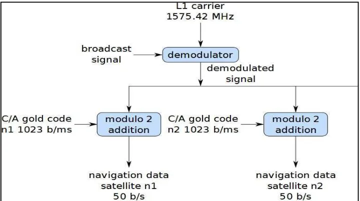
L1 is a civilian-use signal, to be broadcast on the same L1 frequency
(1575.42 MHz) that currently contains the C/A signal used by all current GPS users.
Figure 2.5 shows the demodulating and decoding signals in GPS system
Implementation will provide C/A code to ensure backward compatibility assured of
1.5 dB increases in minimum C/A code power to mitigate any noise floor increase.
Non-data signal component contains a pilot carrier to improve tracking enables
greater civil interoperability with Galileo L1. Figure 2.4 shows the signal that
8
2.5 Demodulation and decoding
Figure 2.3 shows demodulating and decoding signal in GPS System.
Figure 2. 3: GPS satellite transmissions
Figure 2.4 shows the transmission signal from satellite
9
GPS satellites use the microwave L-band to broadcast three separate
radio-navigation signals on two separate RF channels usually called L1 (around 1.6 GHz)
and L2 (around 1.2 GHz). These frequencies were chosen as a compromise between
the required satellite transmitter power and ionospheric errors. The influence of the
ionosphere decreases with the square of the carrier frequency and is very small above
1 GHz. However, in a precision navigation system it still induces a position error of
about 50m at the L1 frequency during daylight and medium solar activity. On the
other hand, GPS were designed to work with omnidirectional,
hemispherical-coverage receiving antennas. The capture area of an antenna with a defined radiation
pattern decreases with the square of the operating frequency, so the power of the
on-board transmitter has to be increased by the same amount.
GPS broadcast two different signals: a Coarse/Acquisition (C/A) signal and
Precision (P) signal. The C/A-signal is only transmitted on the higher frequency (L1)
while the P-signal is transmitted on two widely-separated RF channels (L1 and L2).
Since the frequency dependence of ionospheric errors is known, the absolute error on
each carrier frequency can be computed from the measured difference between the
two P-transmissions on L1 and L2 carries.
The L1 C/A- and P-carriers are in quadrature to enable a single power
amplifier to be used for both signals. The L1 and L2 transmitter outputs are
combined in a passive network and feed an array of helix antennas. These produce a
shaped beam covering the whole visible hemisphere from the GPS orbit with the
same signal strength.
All three GPS transmissions are continuous, straightforward BPSK modulated
carriers. Pulse modulation is not used. The timing information is transmitted in the
modulation: the user's receiver measures the time of arrival of a defined bit pattern,
which is a known code. If desired, the modulation code phase can be related to the
carrier phase in the receiver to produce even more accurate measurements, since both
the carrier frequency and the code rate are derived coherently from the same