UNIVERSITI TEKNIKAL MALAYSIA MELAKA
IDENTIFICATION OF INTERMETALLIC COMPOUND AT
CU WIRE
–
AL BOND PAD INTERFACE BY USING X-RAY
DIFFRACTION
This report submitted in accordance with requirement of the Universiti Teknikal Malaysia Melaka (UTeM) for the Bachelor Degree of Manufacturing Engineering
(Engineering Materials) (Hons.)
by
NOR RAFIKA BINTI NOR HAMID B050910115
900115-05-5110
ABSTRAK
ABSTRACT
DEDICATION
ACKNOWLEDGEMENT
I would like to express my deepest gratitude to my main supervisor Dr. Mohd Warikh bin Abd. Rashid, and also to my co-supervisor Dr. T.Joseph Sahaya Anand lecturer in Faculty of Manufacturing Engineering (Engineering Materials), University Teknikal Malaysia Melaka (UTeM), for their guidance, assistance and concern throughout my research project.
I would also like to extend my sincere thanks to the Mr. Chua Kok Yau who provided me with the extensive discussion and information around my works and interesting exploration in operations.
Special thanks to my friends for giving me supports and helps especially in periods of uncertainties and difficulties. My special thanks are also due to my classmates, Nor Diyanna bt Norazemi and Clement Khoo for their critical suggestions and motivating me throughout in this research.
I am also particularly grateful to the Infineon Company in Melaka for providing me the place to do the research and also to the Engineering Materials Department Laboratory for the facilities.
TABLE OF CONTENTS
List Abbreviations, Symbols and Nomenclatures xi
CHAPTER 1: INTRODUCTION
2.2 Wire Bonding Techniques 8
2.2.1 Thermosonic Bonding Technique 8
2.4.1 Nucleation of IMC 17
2.4.2 IMC Behavior between Cu Bond and Au Bond 20
2.4.3 Mechanism of Nucleation of Intermetallics 22
2.5 Failure Mode of Wire Bonding 22
2.5.1 Cratering on Wire Bonding 22
2.5.2 Kirkendall Effect 24
2.6 Analysis Technique by XRD Analysis 25
2.7 Summary of the Literature Review 29
CHAPTER 3: METHODOLOGY
3.1 Chapter Overview 30
3.2 Materials 32
3.3 Sample Preparation Method 32
CHAPTER 5: CONCLUSION & RECOMMENDATIONS
5.1 Conclusion 53
5.2 Recommendations 54
REFERENCES 55
APPENDICES
A Gantt Chart for PSM I 59
B Gantt Chart for PSM II 60
LIST OF TABLES
LIST OF FIGURES
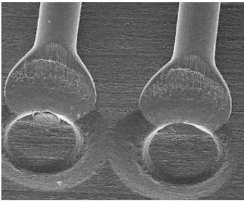
2.1 Ball bonding formation 9
2.2 Wedge bonding formation 9
2.3 A ball wedge interconnection between two bond pads 10
2.4 Schematic procedures of ball-wedge bonding 10
2.5 Capillary tool for ball-wedge bonding 11
2.6a Au wire for ultrasonic bonding; High frequency bond 12 2.6b Au wire for ultrasonic bonding; Low frequency bond 12
2.7 Wedge tool for ultrasonic technique 13
2.8 Schematic procedures for wedge-wedge bonding 14
2.9 IMC coverage and growth of the intermetallics on high temperature storage
18
2.10 Relationship between bonded IMC coverage and probability of ball lift 18 2.11 Cu-Al intermetallics have lower resistivity than Au-Al intermetallics 20 2.12 A cross section of a Cu wire bonded to Al pad shows cratering occurs
under the bond. The wire is slightly lifted and cratering could be seen after chemical etching
22
2.13 Diffractogram of sample in powder form that consists of Cu wires and Si chip
25
2.14 Diffractogram of selected 2θ ranges with slow scan time 26 2.17a Diffractogram of etched powder sample with faster scan 27 2.17b Comparison of diffractogram of unetched and etched powder samples 27
3.1 General overview of the process flow for the study 31 3.2 The process flow for the mechanical removal process for the powder
sample of the Cu-Al IMC
33
3.4 The process flow for the etched sample of Cu-Al IMC 35 3.5 The process flow for the etching optimization process 35
3.6 XRD machine 36
3.7 SEM machine 37
4.1 The collected of the powder samples for Cu-Al IMC 39
4.2 Close view of the Cu-Al IMC parts 40
4.3 Diffractogram for the powder samples of Cu-Al IMC 40 4.4 IMC formation at the ball bond area with a different stress area which (1)
low stress area, (2) and (3) high stress area
41
4.5 Stress distribution under a ball bond during Thermosonic process 42
4.6a EDX analysis for; point 1(low stress area) 43
4.6b EDX analysis for; point 2 (high stress area) 43
4.6c EDX analysis for; point 3 (high stress area) 43
4.7a Condition of the sample; before the etching process 44 4.7b Condition of the sample; after the etching process 44 4.8 The condition of the sample at different etching duration 46
4.9 Percentage of the lifted ball vs time 47
4.10 Diffractogram of the etched samples for Sample 2 (1400s) and Sample 6 (2200s)
48
4.11a Ball bond area for; Sample 2 (1400s) 49
4.11b Ball bond area for; Sample 6 (2200s) 49
LIST OF ABBREVIATIONS, SYMBOLS AND
HTS - High Temperature Storage
IC - Integrated Circuit
SEM - Scanning Electron Microscope
Si - Silicon
SiO2 - Silicon Oxide
TAB - Tape-Automated Bonding
TEM - Transmission Electron Microscope
% - Percentage
° - Degree
1
CHAPTER 1
INTRODUCTION
1.1 Background
There are three main interconnection electrical interconnection methods in intergrated circuit (IC) packages such as flip-chip, tape-automated bonding (TAB), and wire bonding for microelectronic packaging (Murali et al., 2003). Wire bonding technique is the technique that is widely used in industry for making the electrical connection between the chips and the lead frames compared to the other two techniques (Xu et al., 2011). Basically, in wire bonding technique, there are several techniques that have been used in order to make a bonding. The techniques are thermocompression, ultrasonic and thermosonic bonding technique.
pad metallization thus formed a first bond or known as ball bond formation. After that, the wire will make a looping then formed the second bond (wedge bond).
For bonding wire material, Au wire is the most preferred bonding wire material because of its properties which do not oxidize during the process and easily to deform which capable to form a good ball bond. Normally, Au wire is connected to Al bond pad metallization then produced a new phase which is known as intermetallic compound (IMC). However, this bonding system can cause the bond degradation and failure because of the excessive formation of Au-Al IMC and voids (Xu et al., 2011). In order to prevent the failure, thus a Copper (Cu) wire has become a selected wire bond material instead of Au wire since it has many advantages over Au wire. For example, it has high electrical, mechanical and thermal properties and low in terms of cost over Au wire. Other than that, the formation of IMC and void growth is much lower which can prevent from the failure (Xu et al., 2011). For bond pad metallization material, the Al bond pad metallization is the most preferred and suitable in wire bonding industry for decades due to the inexpensive and easily wire bondable.
3
from that, the bonding strength will be increased when the IMCs are formed in the right and proper amount during the wire bonding process, but it will be degraded when the excessive growth of the IMCs are detected (Xu et al., 2009). The IMC formation and growth are basically based on the parameters such as bond force, heat and ultrasonic energy (Chen et al., 2010).
The presence of the IMC formation can be checked by using Optical Microscopy (OM) and Scanning Electron Microscope (SEM). The IMC thickness which is affected by thermal annealing temperatures and times also can be measured by using these two techniques (Kim et al., 2003). The study of the effect of thermal annealing or baking of the Cu-Al IMC has been widely investigated. Basically, these studies relied upon OM and SEM with Energy Dispersive X-ray spectrometry (EDX). However, all the techniques as mention above cannot directly examine the nanostructure and crystallography of the IMC formation (Xu et al., 2011). The detail information is not provided by using those techniques since they are not able to do so, hence the IMC phases of Cu-Al bonds are not clearly identified. In order to get the details of the Cu-Al IMC phase, the Transmission Electron Microscopy (TEM) is used since it is able to analyze the Cu-Al bond interface on the nanoscale and lead to identification of the its crystallographic structure (Xu et al., 2009).
1.2 Problem Statement
much cheaper compared to the Au wire. Other than that, Cu wire will provide better electrical, mechanical and thermal properties (Xu et al., 2011). The growing speed of the Cu-Al IMC is much lower than Au-Al IMC, thus formation of Cu-Al IMC and void growth is much lower over the Au wire. Other than that, the low growing speed of Cu-Al IMC can also lead to a lower electrical resistance and less heat generation hence produced a better reliability and better device performance as well (Zhong, 2011).
The IMC phase at the bonding interface which is in nanometer (nm) scale is affecting the performance or reliability of the microchip, thus detail research is necessary. The IMC growth in a Thermosonic Cu-Al bonding interface is observed to be thin (a few tenth to hundredth nanometers). In this context, one technique has been commonly used which is TEM with EDX and electron diffraction functionality (Xu et al., 2011). TEM technique has been commonly used to obtain the detail information about the IMC morphology and the crystallographic. However, this technique is highly localized and not able to represent the global structure of a bonding interface.
X-ray Diffraction (XRD) technique is a relatively cost effective technique and a promising tool to identify the phase of a specimen. Besides, this technique has been widely used for characterizing thin film and bulk specimen. Other than that, detail information of crystallography and phase identification can be achieved. Nevertheless, there are some challenges while using this technique in order to analyse IMC phase at bonding interface of semiconductor sample. However, a direct measurement of IMC formed at the bonding interface is restricted due to the position of IMC which sandwiches between Cu ball bond and Silicon (Si) substrate. This leads to low intensity of IMC in the diffractogram. Hence, this study is to evaluate two sample preparation methods for the XRD measurement in order to reveal the minor peaks for the Cu-Al IMC phases.
5
1.3 Objectives
The objectives for this study that need to be achieved are:
I. To prepare the sample preparation method for XRD analyis by powder method and etching process for Cu-Al IMC samples.
II. To identify the capability to reveal the minor peak between these two sample preparation methods by using XRD analysis for detecting IMC growth at the bonding interface.
1.4 Scopes of Study
1. Study for the sample preparation method for the powder method. 2. Study on sample preparation for the etching process.
3. Study about the IMC phase at the bonding interface for Cu-Al IMC phases. 4. Study about the XRD analysis for identifying the Cu-Al IMC formation at
1.5 Report Organization
This report will be divided into five major chapters: I. Chapter 1: Introduction
This chapter will explain about the background, problem statement, objectives, and scopes of the study.
II. Chapter 2: Literature review
This chapter will explain with more details which related to the study by referring journals, books or website as sources of the information.
III. Chapter 3: Methodology
This chapter describes the steps on how this study is conducted by making a flow chart of the study. It also explains the procedures of the study that is useful and be as a guideline in order to make the project run smoothly and properly.
IV. Chapter 4: Results and Discussion
This chapter shows the results of the study and discussing the results with more details.
V. Chapter 5: Conclusion
This chapter is the summary of the study. Other than that, some recommendations or suggestions are needed in order to make the future reference.
7
CHAPTER 2
LITERATURE REVIEW
2.1 Wire Bonding
In microelectronic products, current is supplied by the microelectronic packaging towards the IC chips and also distributing the signals between the microelectronic devices. (Zhong et al., 2006). Generally, there are three main electrical interconnection techniques in IC packages that involved in microelectronic packaging such as flip-chip, Tape Automated Bonding (TAB), and wire bonding (Murali et al., 2003). Among these three techniques, wire bonding is said to be the prime technique and widely used in the industry which make a connection between the chips and the lead frames (Hang et al., 2007). Basically, wire bonding is the technique which provides an electrical interconnection between IC chips and lead frames in microelectronics (Xu et al., 2009). Usually Au and Cu wire are used for wire bonding process. The usage of the Au wire is widely used because it does not oxidize during the wire bonding process and make a better contact to the Al bond pad metallization (Zhong et al., 2006). Nevertheless, the cost of Au wire is expensive compared to the Cu wire. Thus, the Cu wire is being selected as the replacement for the Au wire because of its superior properties and low in terms of the cost.
introduced by Bell Laboratories in 1957. This technique was used until the Ultrasonic and Thermosonic bonding techniques were introduced in 1970. In 1963, the first commercial bonding machine was introduced by Kulicke and Soffa Industries for semiconductor industry. Thermosonic Au wire bonding process towards the Al bond pad metallization is the technique that has been widely used in the industry. The energy that is needed in order to make a bonding for this technique is thermal and also ultrasonic energy (Shah et al., 2008). However, many studies of Au-Al IMC phase reported that the bonding strength will be degraded due to the excessive growth of IMC and void formation. Hence, in order to produce a better interconnection reliability, many researchers are focusing on Cu wire for making a replacement for the Au wire (Hang et al., 2007).
Recently the bonding machines used in the industry are operated automatically come with the equipment is also advanced software installed to control the operation of the machine. Most of the wired bonds, 90% are bonded with the Thermosonic bonding technique (ball-wedge bonding) and the rest of the 10% is done with the Ultrasonic bonding technique (wedge-wedge bonding) (Hasnida et al, 2008).
2.2 Wire Bonding Techniques
2.2.1 Thermosonic Bonding Technique
9
Figure 2.1: Ball bonding formation (Murali et al., 2003).
Figure 2.2: Wedge bonding formation (Breach and Wulff, 2009).