Simulation of Wideband Power Amplifier Design for Software Defined
Radio (SDR) Using Feedback and Balanced Topology
A. Salleh
a, M.Z.A Abd Aziz
b, N. R. Mohamad
c, N. M. Z. Hashim
d,
A. S. Ja’afar
eCenter for Telecommunication Research and Innovation (CeTRI), Faculty of Electronic & Computer Engineering, Universiti Teknikal Malaysia Melaka (UTeM), Malaysia
a[email protected], bmohamadzoinol, c[email protected], d[email protected], e
Keywords: Power amplifier, Software Defined Radio, Feedback Topology, ADS, Gain
Abstract. This paper presents the design of power amplifier based on balanced and feedback topology for Software Defined Radio (SDR) using Agilent Advanced Design System (ADS) software. There is a growing interest in SDR in recent years upon the development of new technologies which that capable to support a coverage of Global System for Mobile (GSM), Third Generation (3G) and Wireless Local Area Network (WLAN) at the same location provided by one base station compare to before which is needed a separate base station for different channel bandwidth. The main objective of this research is to design a wideband power amplifier for SDR system that can support wide range frequency from 1.7 GHz to 2.7 GHz using GaAs Enhancement-mode pHEMT transistor from Avago Technologies. The relevant amplifier theory with detailed descriptions of design and simulation processes was discussed in this paper. There are three techniques which are single stage, balanced, and the feedback was used for wideband power amplifier design. In 1 dB compression point for the simulated amplifier, more than 30 dBm of output power, efficiency (PAE) of 50% and gain of 10 dB are achieved. The design based on feedback topology give the highest gain and output power compared to balanced topology.
1. Introduction
Basically, the function of wideband Power Amplifier is to increase the power level which to take a weak signal and make it strong enough to drive a signal especially in transceiver system. However, this wide bandwidth coverage makes the circuit design of key radio frequency (RF) blocks of the front-end transceiver systembecomes more complicated. Therefore, the implementation of wideband RF power amplifier (PA) need to consider the following parameter, such as linearity, efficiency, gain, insertion loss and return loss [1]-[3].
The SDR technology is capable to support a coverage of GSM, 3G and WiMaX at the same location provided by one base station compare to before which is needed a separate base station for different channel bandwidth. It’sadvantages such as inexpensive technique for multimedia, multiband, multifunctional wireless device that can be improved using the software. The main requirement of wideband power amplifier design for SDR is to minimize the costing and small size system [4]-[6]. Currently, the technology was applied in wideband frequency applications including military, commercial and civilian radio [7]-[8]. Communication system face problems using narrowband bandwidth nowadays because this system has multiple power amplifier which is included supporting bias, matching, switch and filter circuitry, so all of these components further increase the cost of production. The wideband technology takes place in a short range communication system instead of narrow-band due to narrowband inability to deal with some
20 13 In tern ation al Con feren ce on Advan ced in Com m un ication Techn ology
Adv ances in Com m unication Technology , Vol.5
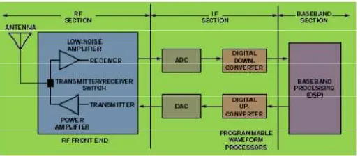
important topics in nowadays technology such as security, high data rate, signal loss, and range resolution [9]. Fig. 1 shows the SDR architecture.
Narrow band technology such as Bluetooth confront with the problem of multipath fading which is described as signal loss due to the destructive interference of continuous wave signals. Moreover, the problem in narrowband is that the signals transmit are insecure because narrowband signals are easily detected and jammed narrowband signals also facing a problem of poor range resolution for tracking applications and limited data rate because narrow RF bandwidth means narrow data bandwidth. The wideband power amplifier is better compare to narrowband power amplifier due to provide the minimum components and overall size[10].
Fig. 1 SDR Architecture
2. Literature Review
The optimal performance of the SDR architecture system is depending on power amplifier design which can be effect to the signal quality, data rate and power efficiency. In the wireless system,the critical issue in the downlink transmission is the efficiency and linearity of power amplifier Thepower amplifier required to operate in back-off area for good linearity which based on error vector magnitude (EVM) parameter. The DC power will increase and introduced the additional thermal dissipated due to low efficiency of power amplifiers. The level of efficiency can be controlled using various linearization methods [11]-16]. Table 1 shows the previous works related to this research.
Table 1 Previous Work of Power Amplifier Design Author Frequency
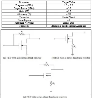
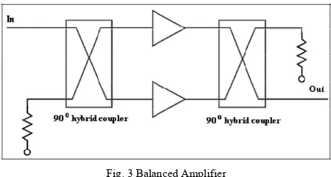
maximum efficiency. There are various techniques that can be used to achieve a wider bandwidth. In this section, the three most common bandwidth enhancement techniques were used which is reactive matching, lossy matching, balanced amplifier and feedback amplifier [3]-[4]. Feedback topology offers can increase stability in the amplification, reduces distortion, easier to achieve desired input and output impedances and achieve wide bandwidth. In addition, it can improve the input and output match, and stability by reducing the gain at low frequencies. However, the feedback resistor consumes power, and so it should be able to dissipate the heat. For power output designs, such as in this research, the feedback approach is most suitable. Consider the transistor with series-shunt feedback resistors and Fig. 2 shows some kinds of feedback networks. However, the input and output matching will improve with constant gain response by using a balanced amplifier technique as shown in Fig. 3. The input and output reflections from two identical amplifier can be reduced using two 90º couplers.
Table 2 Specification of Power Amplifier
Parameter Target/Value
Frequency (GHz) 1.7 – 2.7
Output Power (dBm) > 30
Gain (dB) > 10
Efficiency (%) > 50
Transistor GaAs Phemt
Noise Figure < 1
Matching Network Single Stub
Topology Balanced and Feedback Amplifier
Fig. 3 Balanced Amplifier
Unconditional stability of the circuit is another important parameter in designing of power amplifier, this characteristic means that the device does not oscillate over a range of frequencies with any combination of source and load impedance. The stability is depending on Rollet’s stability factor, K and ∆ which shown in Eq. 1 and Eq. 2.
Next, the purpose of biasing is so that the amplifier design can operate at the selected biasing point which is gate voltage, VGSand current, I. The biasing network must be able to hold the operating point constant over variations in temperature and device parameters. The biasing process obtained the transistor static IV curves for the desired amplifier classes such as Class A, AB, B, or C which the Class A is chosen to get the optimum load line on the IV curve. The purpose of adding the matching network to the system is to provide the maximum delivery to the load of the RF power available from the source. Matching network is typically placed between the transmission line and load which ideally lossless and able to avoid unnecessary loss of power. There are several types of matching technique such as matching with lumped elements, single stub matching and quarter wave transformer [2]. The input and output impedances must be matched to the source and the load impedances to prohibit reflections and to maximize power transference. The matching will also have a lot to stay for the bandwidth. The power transference will reach the maximum when the input impedance of the amplifier is the complex conjugated to the source impedance, and the output impedance is complex conjugated to the load impedance.
The simulation involved was done by using Advanced Design System (ADS) software which including the simulation of two portnetworks based on S – Parameters, noise figure, gain in the power amplifier design such as power gain, transducer gain, available gain and maximum gain, and the stability test to make sure the design is stable. After all the needed specifications achieved, all the circuits like DC biasing circuit, equivalent input and output matching circuit, complete power amplifier design circuit and its optimization will also simulate in the ADS software. This will also involve the process of optimization which to improve the performance of power amplifier.
4. Result and Analysis
of IV characteristic of the transistor which the optimal condition of the bias point can be determined and to avoid from self damage due to thermal heating. The optimal performance of the transistor can be simulated in the ADS software by using the ZAP file provided by the Avago Technology.
Fig. 4 IV Characteristic
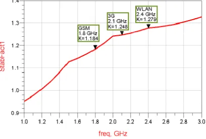
The stability can be determined from the value of K and Δ. Below is the calculation for the frequency of 2.0 GHz. Thus the K > 1 and Δ < 1, indicate that the stability criteria of the transistor areunconditionally stable which satisfied the amplifier stability for all passive sources and load impedance. Fig. 5 shows the simulation results of the stability factor K.
Fig. 5 Simulation of Stability Factor, K
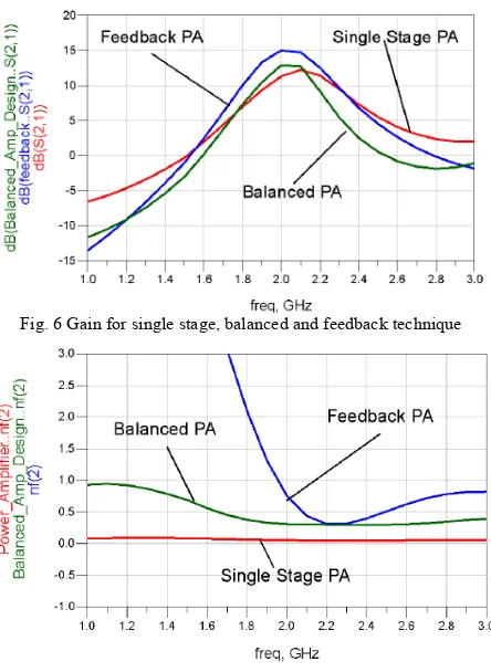
Fig. 6 shows the gain for single stage design, balanced and feedback technique. The gain, S21 for the channel GSM, 3G and WLAN of feedback power amplifier is 7.332 dB, 12.412 dB and 5.662 dB respectively. Gain, S21 for the balanced amplifier is 9.122 dB, 11.382 dB and 0.570 dB
Fig. 6 Gain for single stage, balanced and feedback technique
Fig. 7 Noise Figure for single stage, balanced and feedback technique
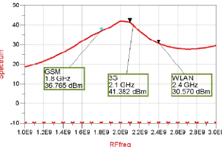
Fig. 9 Output power of the feedback technique
5. Conclusion
The wideband power amplifier was successfully designed using balanced and feedback topology for the SDR system which that can support wide range frequency from 1.7 GHz to 2.7 GHz. The RF power amplifier design is one of the critical part in overall system of SDR. The design of wideband amplifier introduces new difficulties which require a lot of considerations such as linearity, efficiency, gain, output power, insertion loss and return loss. The implementation of wideband power amplifier for SDR technology provides minimum costing with small size and less components which need to maintain the efficiency and linearity of the amplifier. The feedback amplifier has the best gain and output power comparing to balance amplifier. Feedback technique is being used to achieve wide bandwidth, improve the input and output match, and stability by reducing the gain at low frequencies. A layout design and a prototype should be made to evaluate the accuracy of the simulations. In the future, design technique that gives the best performance will be fabricated in the board so that the analysis between the simulation and the real result of the measurement of the product can be made.
6. Acknowledgement
The author would like to thank Universiti Teknikal Malaysia Melaka (UTeM) for thefund to complete this research.
References
[1] M.H. Misran, M.A. Meor Said, A.Salleh, M.A. Othman, M.M. Ismail, H.A. Sulaiman, R.A.
Ramlee, Design of Low Noise Amplifier for Wimax Application, IOSR Journal of Electrical and Electronics Engineering (IOSR-JEEE) e-ISSN: 2278-1676,p-ISSN: 2320-3331, Volume 6, Issue 1 (May. - Jun. 2013), PP 87-96.
[2] A. Salleh, N. R. Mohamad, M. Z. A Abd Aziz, N.M. Z Hashim, M. H. Misran, M. A. Othman, Design the High Gain and Low Power Amplifier for Radio over Fiber Technology at 2.4 GHz, American Journal of Engineering Research (AJER), Volume-02, Issue-09 (2013), pp.163-170.
[4] A. Salleh, K. S. Yong, M. Z. A. Abd Aziz, M. H. Misran, N. R. Mohamad, Design of Low Power Wideband Low Noise Amplifier for Software Defined Radio at 100 MHz to 1 GHz, Procedia Engineering 53 ( 2013 ) pp. 368 – 375.
[5] A. Salleh, M. Z. A. Abd Aziz, M. H. Misran, M. A. Othman, N. R. Mohamad, Design of
Wideband Low Noise Amplifier using Negative Feedback Topology for Motorola Application, Journal of Telecommunication Electronic and Computer Engineering (JTEC), Vol. 5 No. 1 (January-June 2013).
[6] A. Salleh, M. Z. A Abd Aziz, N. R. Mohamad, M. A. Othman, Z. Zakaria, M. H. Misran, Design of Low Noise Amplifier for Radio over Fiber at 5.2 GHz, IOSR Journal of Electronics and Communication Engineering (IOSR-JECE), Volume 5, Issue 3 (Mar. - Apr. 2013), pp. 65-69.
[7] Walter Tuttlebee, Software Defined Radio: Enabling Technologies, Walter H.W Tuttlebee
(2002), pp.1-2.
[8] Jeffrey H.Reed, Software Radio: A Modern Approach to Radio Engineering, Prentice Hall
(2002), pp.36-56.
[9] Rameswor Shrestha, RF Power Amplifier Techniques For Spectral Efficiency And Software-Defined Radio, University of Twente, (2010) pp.1-133.
[10]Asad A. Abidi, The Path To The Software-Defined Radio Receiver, IEEE Journal of Solid-State Circuits, Vol. 42, No. 5 (2007),pp.994-966.
[11]M. Dillinger, K. Madani, and N. Alonistioti, Eds., Software Defined Radio: Architectures, Systems and Functions. Hoboken, NJ: Wiley, 2003.
[12]F. K. Jondral, Software-defi ned radio: Basics and evolution to cognitive radio, EURASIP J. Wireless Commun. Networking, vol. 2005, no. 3, pp. 275–283.
[13]F. H.Raab, P.Asbeck, S.Cripps, P.B.Kenington, Z.B.Popovic, N.Pothecary, et al., Power amplifiers and transmitters for RF and microwave, IEEE Trans. Microwave Theory Tech., vol.50, no.3 (2002), pp. 814–826.
[14]D.Rudolph, “Kahn EER technique with single-carrier digital modulations,”IEEE Trans. Microwave Theory Tech.,vol.51 (2003), no.2, pp. 548–552.
[15]D.C.Cox, et al., “Component signal separation and recombination for linear amplification with non linear components,” IEEE Trans. Communication., pp.1281–1293, Nov.1975.
[16]J.R.Gajadharsing, O.Bosma, and P.Van Westen, Analysis and design of a 200W LDMOS based Doherty amplifier for 3G base stations, Proc. of IEEE MTT-S Int. Microwave Symp. Dig., vol. 2 (2004), pp. 529–532.
[17]Muhammed Hakan Yilmaz, Design of a wideband 10W GaN power amplifier, Norwegian
University of Science and Technology, July 2011.
[18]Choi Hing Cheung, RF Power Amplifier – Class F Power Amplifier, The Chinese University of Hong Kong, May 2007.
[19]Yi-Jan Emery Chen, “An Integrated Wideband Power Amplifier for Cognitive Radio”,