GENERATION HVDC AND TEST ON INSULATOR (PLYWOOD)
MOHD RAZIF BIN ISMAIL B010410143
“I hereby declare that I have read through this report and found that it has comply the partial fulfillment for awarding the degree of Bachelor of Electrical Engineering
(Industrial Power)”
Signature : ………
Supervisor‟s Name : ………
GENERATION HVDC AND TEST ON INSULATOR (PLYWOOD)
MOHD RAZIF BIN ISMAIL
This Report Is submitted In Partial Fulfillment Of Requirement For The Degree of Bachelor In Electrical Engineering (Industrial Power)
Fakulti Kejuruteraan Elektrik Universiti Teknikal Malaysia Melaka
“I hereby declare that this report is a result of my own work except for the experts that have been cited clearly in the reference.”
Signature : ………
Name : ………
ACKNOWLEDGEMENTS
First of all, I would like to thank Allah, who has give me a chance and strength to complete my Projek Sarjana Muda 2, „Generation HVDC and Test on Insulator (plywood)‟ and my report. I would like to thank Universiti Teknikal Malaysia Melaka (UTeM) especially Faculty of Electrical Engineering(FKE) for give an opportunity to do my Projek Sarjana Muda 2 (PSM 2) in fulfillment for Bachelor of Engineering.
Then, I would to thank my supervisor, Pn Jurifa binti Mat Lazi for supervising me when doing this project and giving me full support and teach me whatever I did not know. I also would like to thanks to En. Alias and En Hidayat because always give idea about this project.
ABSTRACT
ABSTRAK
CHAPTER CONTENT PAGE
5 SAFETY AND STANDARD MANUAL PROCEDURE
LIST OF TABLE
NO CONTENT PAGE
3.1 Simulation Result for First Stage 11
3.2 Simulation Result for Two Stage 13
3.3 Simulation Result for Three Stage 15 4.1 Type and Description of the Main Component 18 4.2 Generation Result for DC 1 Stage 21 4.3 Generation Result for DC 2 Stages 21 4.4 Generation Result for DC 3 Stages 21 4.5 Result for First Stage at Point A 23 4.6 Result for First Stage at Point B 23 4.7 Result for First Stage at Point C 24
4.8 Result for 2 Stage at Point A 25
4.9 Result for 2 Stage at Point B 26
LIST OF FIGURE
NO CONTENT PAGE
2.1 Half Wave Rectifier 6
2.2 Basic Circuit of Half Wave Rectifier 6 2.3 Basic Waveform for Half Wave Rectify 6
2.4 Two Stages Voltage Multiplier 7
3.1 Project Circuit Simulation for First Stage 10 3.2 Project Circuit Simulation for Two Stage 12 3.3 Project Circuit Simulation for Three Stage 14 4.1 Equipment Setup for Multi Stages 19
4.2 DC 1 stage Configuration 19
4.3 DC 2 stage Configuration 20
4.4 DC 3 stage Configuration 20
4.5 Test Bed 22
4.6 Breakdown Voltage Plywood on First Stage 25 4.7 Breakdown Voltage Plywood on Two Stage 27
6.1 Project Flowchart 45
6.2 Simulation Flowchart 46
LIST OF ABBREVIATION
DMI - Digital Measuring Instrument
ANSI - American National Standard Institute OT - Operating Terminal
IEEE - Institute of Electrical and Electronics Engineers IEC - International Electrotechnical Commission
LIST OF APPENDIX
TOPIC PAGE
IEEE Standard 51
Equipment 69
CHAPTER I
INTRODUCTION
1.1 Introduction of High Voltages
The International Electrotechnical Commission (IEC) and its national counterparts (IET, IEEE, VDE, etc.) define high voltage circuits as those with more than 1000V for alternating current and at least 1500V for direct current, and distinguish it from low voltage (50–1000V AC or 120–1500V DC) and extra low voltage (<50V AC or <120V DC) circuits. This is in the context of the safety of electrical apparatus.
In the United States 2005 National Electrical Code (NEC), high voltage is any voltage over 600V. British Standard BS 7671:2008 defines high voltage as any voltage difference between conductors that is higher than 1000V AC or 1500 V ripple-free DC, or any voltage difference between a conductor and Earth that is higher than 600 V AC or 900 V ripple-free DC.
The general public may consider household mains circuits (100–250V AC), which carry the highest voltages they normally encounter, to be high voltage. For example, an installer of heating, ventilation and air conditioning (HVAC) equipment may be licensed to install 24V control circuits, but may not be permitted to connect the 240V power circuits of the equipment.
1.2 Problem Statement
Haefley High Voltage Test Set is the new equipment that available in the High Voltage Lab at Faculty Of Electrical Engineering. Since the equipments are not tested yet, it is necessary to analysis the characteristic and specification in order to apply in the laboratory for learning process. The testing procedures and safety precaution should be prepared because it involved the high voltage up to 100kV for first stage, up to 280kV for second stage and up to 400kV for third stage. This project will use both simulations using LTspice which has been done in the PSM 1 and the real test involving test objects in the PSM 2.
For time being there have been various problem especially related with the equipment. The major problem that has to be highlighted is the oscilloscope. The provided oscilloscope does not meet the requirement to be used with the Haefely high voltage set. However for PSM 2 there is a new oscilloscope from Tektronik which is much advance and the waveform can be captured much easier. But there‟s still a problem as did not have enough time to maximize the usage of it for much advance task. For time being we only able to use it for basic waveform capturing tasks.
The main purpose of test object is to get breakdown voltage for the object. Breakdown voltage is important in electrical field especially to make insulator. Plywood has been chosen for this test because this objects easy to find and have potential as an insulator.
Limited knowledge of the equipment also makes it hard to do the lab test and other testing especially when it involves testing it to other object like cables. The standard used for the High Voltage Test is also unspecific and has a lot of unknowns especially for the students. There is also no specific reference regarding to the project title and the only available references is based on the cables and other high voltage equipments.
Simulations are hard to be done as there‟s not much simulations software for high voltage analysis related to this equipment. Besides there‟s also unknown quantity at of high voltage diode breakdown voltage.
1.3 Objective
The objectives of this project are:
1. To develop the high voltage testing procedures and safety precaution for high voltage lab purpose.
2. To simulate Hafl Wave rectifier and Greinacher Doubler circuit using LT Pspice.
3. To study and analyze the characteristics of high voltage DC configuration. 4. To test object (plywood) while do experiment.
5. To compare the result data between experimental
1.4 Scope
This project scope is to learn the theory of produce DC high voltage from „Greinacher Doubler-Circuit‟ and to make the experiment base on HEAFELY kit. Besides that, this project also needs to make simulation for compare the data between experiment and simulation.
1.5 Thesis Outline
Chapter 1 is basically the introduction part of the project chosen. In this chapter, the project background and problems statements will be discussed clearly. Besides, the project objectives and project scope will be explained details so that a better view of the project can be obtained.
circuit. As for this project, the high d.c. voltage can be generated using the half wave rectifier circuit. In this chapter also will discussed IEEE standard technique to test insulator using high voltage.
In chapter 3, simulation using LT Pspice will be showed. In this chapter, Half Wave rectifier circuit will be used for simulation first stage. For second and third stages, Greainacher Doubler circuit will be used for simulation.
In chapter 4, this chapter will discuss about experimental setup using HEAFELY KIT. All components will be listed and all block diagrams for three stages will show. This chapter also has explanation about test object (plywood). The result for generation and test object will be analysis.
CHAPTER II
LITERATURE REVIEW
2.1 High Direct Current Voltage
Generation of high DC voltages is mainly requited in research work in the areas of pure and applied physics. Sometimes, high direct voltages are needed in insulation tests on cable and capacitor. Usually, for generate DC voltage up to 100kV, electronic valve rectifiers are used and the outputs current are about 100mA. There have several ways to produce high DC voltage:
1. Half wave rectifier 2. Full wave rectifier
3. Voltage doubler rectifier type
These entire type rectifier convert AC voltage to high DC voltage using power diode. For this project, Half Wave rectifier will be used at single stage and Greinacher Doubler-Circuit will be used for second and third stages.
2.1.1 Half Wave Rectifier
A half wave rectifier is a special case of a clipper. In half wave rectification, either the positive or negative half of the AC wave is passed easily, while the other half is blocked, depending on the polarity of the rectifier. Because only one half of the input waveform reaches the output, it is very inefficient if used for power transfer. Half-wave rectification can be achieved with a single diode in a one phase supply.
Figure 2.1: Half Wave rectifier
Figure 2.2: Basic circuit of Half Wave rectifier
2.1.2 Greinacher Doubler-Circuit
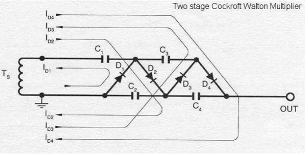
One of the cheapest and popular ways of generating high voltages at relatively low currents is the classic multistage diode/capacitor voltage multipler, known as Greinacher Doubler-Circuit or Cockcroft Walton multiplier. This circuit was invented by Heinrich Greinacher, a Swiss physicist at 1919.
The Cockcroft Walton or Greinacher design is based on the Half-Wave Series Multiplier, or voltage doubler. In fact, all multiplier circuits can be derived from its operating principles. It mainly consists of a high voltage transformer Ts, a column of smoothing capacitors (C2,C4), a column of coupling capacitors (C1,C3), and a series connection of rectifiers(D1,D2,D3,D4). The following description for the 2 stage CW multiplier assumes no losses and represents sequential reversals of polarity of the source transformer Ts in the figure 2.4. The number of stages is equal to the number of smoothing capacitors between ground and OUT, which in this case are capacitors C2 and C4.
Figure 2.4: Two Stages Voltage Multiplier
Figure 2.4 show the circuit flow start from transformer Ts, negative peak, C1
charges through D1 to Epk at current ID1. While Ts at positive peak, Epk of Ts adds
arithmetically to existing potential C1, thus C2 charges to 2Epk through D2 at current
ID2. This cycle continue with negative peak, C3 is charged to Epk through D3 at
current ID3. While Ts positive peak, C4 is charged to 2Epk through D4 at current ID4.
2.2 IEEE Standard Technique For High-Voltage Testing
The test on insulators can be divided into three groups. These are the type test, and sample test
Test type
These tests are done to determine whether the particular design is suitable for the purpose.
a) Withstand test
The insulators should be mounted so as to simulate practical condition. A 1/50 µs wave of the specified voltage (corrected for humidity, air density) is applied. Flashover or puncture should not occur ( if puncture occur, the insulator is permanently damage). The test is repeated five times for each polarity.
b) Flash-over test
1/50 µs wave is applied. The voltage is gradually increased to the 50% impulse flashover voltage. There should be no puncture of insulation during these tests.
c) Dry one-minute test
The insulator clean and dry should be mounted as specified and prescribed voltage (corrected for ambient condition) should be gradually brought up (at power frequency) and maintained for one minute. Thee shall not be puncture or flash over during the test.
d) One-minute Rain test
The insulator is sprayed throughout the test with artificial rain drawn from a source of supply at a temperature within 10oc of the ambient temperature of the
neighborhood of the insulator. The rain is sprayed at an angle of 45o on the insulator
e) Visible discharge test
This states that after the room has been darkened and the specified test voltage applied, after five minutes, there should be no visible signs of corona.
Sample tests
The sample is tested fully, up to and including the point of breakdown. This is done only on a few samples of the insulator.
a) Temperature cycle test
The complete test shall consist of five transfers, each transfer not exceeding 30 s.
b) Mechanical loading test
The insulator should be mechanically loaded up to the point of failure. When failure occurs, the load should not be less than 2000 lbf.
c) Electro-mechanical test
The insulator is simultaneously subjected to electrical and mechanical stress. It will be subjected to a power frequency voltage and a tensile force simultaneously. The voltage shall be 75% of dry flashover voltage of the unit. There should be no damage caused.
d) Over voltage test
The insulator should be completely immersed in an insulating medium (oil), to prevent external flashover occurring. The specified overvoltage must be reached without puncture. The voltage is then gradually increased until puncture occurs.
e) Porosity test
CHAPTER III
SIMULATION
3.1 Introduction
Switchercad III LTspice by Linear Technology is a freeware and much easier to be understand. This software is downloaded from the Linear Technology website at www.linear.com/company/software.jsp. This software has the same ability as the PSpice software but with an advantage over easiness of use and simpler interface.
3.2 Stage 1 simulation
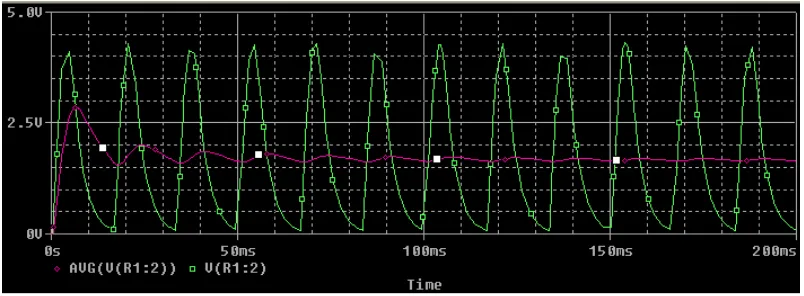
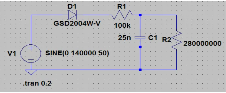
The project circuit was simulated using the LT Spice software. As mention before, the project circuit is a half wave rectifier circuit. The input voltage, V1 is set to140 kVAC p-p that equal to 100 kVAC rms. The GSD2004W-V is a HV rectifier that will change the alternating current (AC) to direct current (DC) and this process is normally known as rectification.
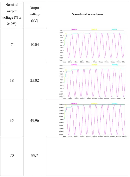
Table 3.1: Simulation result for first stage
Nominal output voltage (% x
240V)
Output voltage
(kV)
Simulated waveform
7 10.04
18 25.02
35 49.96