i THE IMPACT OF SILICON BODY THICKNESS ON DEVICE
PERFORMANNCE OF 18nm LOW POWER SILICON ON INSULATOR
NUREZZATY BINTI JAMALUDDIN
This Report Is Submitted In Partial Fulfilment Of Requirement For The Bachelor Degree Of Electronic Engineering (Computer Engineering) With Honours
FAKULTI KEJURUTERAAN ELEKTRONIK DAN KEJURUTERAAN KOMPUTER
UNIVERSITI TEKNIKAL MALAYSIA
v
ACKNOWLEDGEMENT
Prima facie, I am grateful to almighty Allah for the good health and His blessing that allow me to complete my final year project in order to graduate in Bachelor of Electronic Engineering (Computer Engineering) with honour. Without His pleasure and kindness, as His servant, I am incapable of doing anything
My biggest gratitude to my supervisor Dr. Anis Suhaila Binti Mohd Zain, whose accept me the way I am to be one of her student. Thank you for her
understanding and patience in order to teach and help me in completing this project. For all her courage and motivations that being given will be used wisely in facing the future. Big thanks because willing to share your life experience in life that makes me to realise that to be successful person, there must be a bitter challenges. Last but not least for my respected supervisor, I am happily to hear your life story about your children and may Allah bless your family into jannah.
Sincerely thanks to my academic supervisor Dr. Fauziyah Binti Sallehuddin that help me in 3 years’ time while I am study here. Thanks for all your support in my study that sometimes becomes up and down but you still remind me to keep being positive and strive for the success. All your help is much appreciated and all I can say is I hope Allah ease you in everything and grant you jannah.
I would also thanks to Faculty of Electronic and Computer Engineering for providing the facilities for all this years I being study here. Hopefully all the facilities will be upgraded time to time in order to provide a conducive learning environment for student in future. Hopefully by that, this faculty could produce more greater and successful engineers.
vi
ABSTRACT
vii
ABSTRAK
viii
TABLE OF CONTENT
CHAPTER TITLE PAGE
PROJECT TITLE i
DECLARATION STATUS OF REPORT FORM
ii
DECLARATION iii
SUPERVISOR DECLARATION iv
ACKNOWLEDGEMENT v
ABSTRACT vi
ABSTRAK vii
TABLE OF CONTENT viii
LIST OF FIGURES xi
LIST OF APPENDIX xiii
TABLE OF CONTENT xvi
I INTRODUCTION
1.1 Project Introduction 1
1.2 Problem Statement 2
1.3 Objective 2
ix
II LITERATURE REVIEW
2.1Silicon on Insulator (SOI) 4
2.2Miniaturization 5
2.3Moore’s Law 6
2.4Silicon Body Thickness 7
2.5SOI Scaling Effect 8
2.5.1Threshold voltage 8
2.5.2Leakage Current 9
2.5.3Internal Resistance 10
2.5.4Self-Heating 10
2.5.5Sub-Threshold Slope 11
2.6Comparison between SOI MOSFET and Bulk MOSFET
11
2.6.1Advantages of SOI MOSFET 12
III METHODOLOGY
3.1Overview Project Development Flowchart 14 3.2 Flowchart for SOI MOSFET Designing Process 15 3.3 Flowchart for Extracting and Displaying
Tonyplot Graph
17
I V RESULT AND DISCUSSION
4.1 Introduction 18
4.2 Structure and extracting parameters of SOI MOSFET using 7.6nm body thickness
24
4.3Structure and extracting parameters of SOI MOSFET using 7.4nm body thickness
29
x MOSFET using 7.2nm body thickness
4.5 Structure and extracting parameters of SOI MOSFET using 6.4nm body thickness
39
4.6 Description of overall design parameter 44 4.7 Comparison and analysis of result. 45
V CONCLUSION AND RECOMMENDATION
5.1 CONCLUSION 48
xi
LIST OF TABLE
NO TITLE PAGE
4.1 High Voltage Parameter Design for 7.8nm Silicon Body Thickness 20
4.2 Extracted Result for High Drain Voltage for 7.8nm Silicon Body Thickness 21
4.3 Low Voltage Parameter Design for 7.8nm Silicon Body Thickness 22
4.4 Extracted Result for Low Drain Voltage for 7.8nm Silicon Body Thickness 23
4.5 High Voltage Parameter Design for 7.6nm Silicon Body Thickness 25
4.6 Extracted Result for High Drain Voltage for 7.6nm Silicon Body Thickness 26
4.7 Low Voltage Parameter Design for 7.6nm Silicon Body Thickness 27
4.8 Extracted Result for Low Drain Voltage for 7.6nm Silicon Body Thickness 28
4.9 High Voltage Parameter Design for 7.4nm Silicon Body Thickness 30
4.1 Extracted Result for High Drain Voltage for 7.4nm Silicon Body Thickness 31
4.11 Low Voltage Parameter Design for 7.4nm Silicon Body Thickness 32
4.12 Extracted Result for Low Drain Voltage for 7.4nm Silicon Body Thickness 33
xii
4.14 Extracted Result for High Drain Voltage for 7.2nm Silicon Body Thickness 36
4.15 Low Voltage Parameter Design for 7.2nm Silicon Body Thickness 37
4.16 Extracted Result for Low Drain Voltage for 7.2nm Silicon Body Thickness 38
4.17 High Voltage Parameter Design for 6.4nm Silicon Body Thickness 40
4.19 Low Voltage Parameter Design for 6.4nm Silicon Body Thickness 42
4.2 Extracted Result for Low Drain Voltage for 6.4nm Silicon Body Thickness 43
xiii
LIST OF FIGURES
NO TITLE PAGE
2.1 Bulk MOSFET 4
1.2 SOI MOSFET 5
2.3 Challenge in Chips Development 6
2.4 Silicon body thickness as manipulated parameter in this project
7
2.5 Self-heating effect in SOI 10
2.6 Improvement in execution time by using SOI 12
3.1 Project Methodology Flowchart 14
3.2 Structure Design Flowchart 16
3.3 Extracting Parameters Flowchart 17
4.1 SOI design with 7.8nm body thickness 19
4.2 Contour structure of 7.8nm body thickness 19
4.3 Linear Drain current (Id) Vs. Gate Voltage (Vg) for 7.8nm silicon body thickness(High Voltage)
20
4.4 Log Drain current (ID) vs. Gate Voltage (Vg) for 7.8nm silicon body thickness (High Voltage)
21
4.5 Linear Drain current (ID) Vs. Gate Voltage (Vg) for 7.8nm silicon body thickness (Low Voltage)
22
4.6 Log Drain current (ID) Vs. Gate Voltage (Vg) for 7.8nm silicon body thickness (Low Voltage)
24
4.7 SOI design with 7.6nm body thickness 24
4.8 Contour structure of 7.6nm body thickness 24
xiv silicon body thickness (High Voltage)
4.10 Log Drain current (ID) vs. Gate Voltage (Vg) for 7.6nm silicon body thickness (High Voltage)
26
4.12 Linear Drain current (ID) vs. Gate Voltage (Vg) for 7.6nm silicon body thickness (Low Voltage)
27
4.12 Log Drain current (ID) vs. Gate Voltage (Vg) for 7.6nm silicon body thickness (Low Voltage)
28
4.13 SOI design with 7.4nm body thickness 29
4.14 Contour structure of 7.4nm body thickness 29
4.15 Linear Drain current (ID) vs. Gate Voltage (Vg) for 7.4nm silicon body thickness (High Voltage)
30
4.16 Log Drain current (ID) vs. Gate Voltage (Vg) for 7.4nm silicon body thickness (High Voltage)
31
4.17 Linear Drain current (ID) vs. Gate Voltage (Vg) for 7.4nm silicon body thickness (Low Voltage)
32
4.18 Log Drain current (ID) vs. Gate Voltage (Vg) for 7.4nm silicon body thickness (Low Voltage)
33
4.19 SOI design with 7.2nm body thickness 34
4.20 Contour structure of 7.2nm body thickness 34 4.21 Linear Drain current (ID) vs. Gate Voltage (Vg) for 7.2nm
silicon body thickness (High Voltage)
35
4.22 Log Drain current (ID) vs. Gate Voltage (Vg) for 7.2nm silicon body thickness (High Voltage)
36
4.23 Linear Drain current (ID) vs. Gate Voltage (Vg) for 7.2nm silicon body thickness (Low Voltage)
37
4.24 SOI design with 6.4nm body thickness 39
4.25 Contour structure of 6.4nm body thickness 39 4.26 Linear Drain current (ID) vs. Gate Voltage (Vg) for 6.4 nm
silicon body thickness (High Voltage)
40
4.27 Log Drain current (ID) vs. Gate Voltage (Vg) for 6.4nm silicon body thickness (High Voltage)
41
xv silicon body thickness (Low Voltage)
4.29 Log Drain current (ID) Vs. Gate Voltage (Vg) for 6.4nm silicon body thickness (Low Voltage)
43
4.24 SOI design with 6.4nm body thickness 39
4.25 Contour structure of 6.4nm body thickness 39 4.26 Linear Drain current (ID) vs. Gate Voltage (Vg) for 6.4 nm
silicon body thickness (High Voltage)
40
4.27 Log Drain current (ID) vs. Gate Voltage (Vg) for 6.4nm silicon body thickness (High Voltage)
41
4.28 Linear Drain current (ID) vs. Gate Voltage (Vg) for 6.4 nm silicon body thickness (Low Voltage)
42
4.29 Log Drain current (ID) Vs. Gate Voltage (Vg) for 6.4nm silicon body thickness (Low Voltage)
43
4.25 Contour structure of 6.4nm body thickness 39 4.26 Linear Drain current (ID) vs. Gate Voltage (Vg) for 6.4 nm
silicon body thickness (High Voltage)
xvi
LIST OF APPENDIX
NO TITLE PAGE
A Coding For Design Structure 54
1
CHAPTER I
INTRODUCTION
1.1. Project Introduction
MOSFET is used as a switching device in electronic world. Year by year, the size as be continuously scaled down to make the transistor smaller to pack more and more devices in a given chip area. Smaller physical size can make transistor switching process faster compare to larges size. The main part that been normally scaled are channel length, channel width, and oxide thickness. However, the more the size had been reducing, many problems occur during designing the MOSFET.
SOI has been introduced in 1980s in order to improve the SIMOX technology. The silicon layer thickness can be in range in micron which is very small in size. With SOI technology it can increase chip functionality without big changes of the design. Silicon on insulator consists of three main layer silicon body, buried oxide (BOX) and bulk. The difference between SOI MOSFET and bulk MOSFET is the existing of the BOX layer between the silicon body and the bulk. SOI is a planar process technology that relies on primary innovation which is ultra-thin layer of insulator called the buried oxide that positioned on top of the base silicon.
2
latch up. The leakage current more smaller in SOI structure in order to apply for low standby power device such as a mobile phone. [1]
This project will focus on impact of silicon body thickness on device performance of 18nm gate length for low power application. Refer to 2011 overall roadmap technology characteristic (ORTC) by ITRS the parameter changes in every year. The main focus in this project is reducing the body thickness because it is has potential for ultimate scaling of MOSFET. Besides that, it can improve the power consumption, threshold voltage and current. But, reduction of body thickness will lead to transistor gate leakage current and change the slope of threshold voltage as it affected by deducting of SOI body thickness.
1.2. Problem Statement
Semiconductor industry never fails to undergo improvement of device in every year consistent with advancement in nowadays technology. Scaling down size of device is major topics in semiconductor industry due to many problems occur such as large current leakage, increases of threshold voltage and increase of internal resistance. In this project, all the problems will be given more attention in order to gain a better device.
1.3. Objective
1. To design and simulate the SOI with reduction of silicon body thickness by using ATHENA and ATLAS from SILVACO.
2. To analyse the impact of silicon body thickness on device performance using 18nm gate length.
3
1.4. Scope
4
CHAPTER II
LITERATURE REVIEW
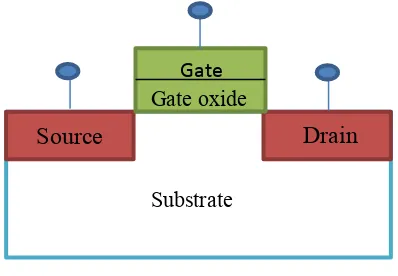
2.1Silicon on Insulator (SOI)
Research on SOI has been done about two decades in order to have better device performance for electronic industry [3]. Structure of SOI is not much different compared to normal bulk MOSFET. The major difference is the insertion of insulation layer beneath on device [2]. SOI MOSFET is the evolution of bulk MOSFET in order to overcome the problem that occurs in bulk MOSFET. SOI is becoming mainstream technology for future high performance and low power application. SOI contains three main layer which are body silicon, buried oxide (BOX) and bulk. BOX is a new layer that makes the major difference between SOI and bulk MOSFET as shown in figure 2.1.
Figure 2.1: Bulk MOSFET Gate Gate oxide
Source Drain
5
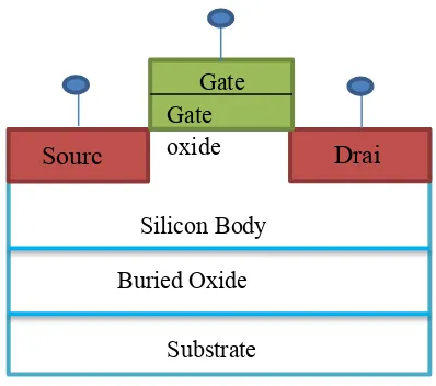
Figure 1.2: SOI MOSFET
2.2Miniaturization
SOI is one of manufacturing strategies to miniaturize of microelectronic device. A long before SOI technology been introduced, bulk MOSFET has been continuously scaled down in size for the purpose to make the transistor smaller so that more chips can be placed on the wafer. The benefit of the miniaturization size can lead to slowing down the price per chip at the same time still has the same function as before. In fact the number of transistor per chip has been double every 2 to 3 years [4].
It already proved that smaller transistor will switch faster. So that, the reduction of size will scale down overall MOSFET parameters involving it channel length, channel width and the thickness of overall body. Year by year the size of MOSFET is getting smaller and many difficulties arises such as higher sub-threshold voltage is needed but the shrinking of size will reduce the voltage in order to maintain the reliability. As for that, sub-threshold voltage also been reduce but the problem occurs because the transistor cannot be switched from turn off to turn on. The MOSFETs also face with increases of junction leakage, lower output resistance and interconnect capacitance [2]. Research have found that SOI MOSFET could overcome the problem occurs in bulk MOSFET.
Gate Gate oxide
Sourc Drai
Substrate Buried Oxide (BOX)
6
After SOI MOSFET is been introduced SOI technology also begins to shrink down to fulfil the market demands. Shrinking down the size will lead to several problems as many layer and part of the transistors already changed. It is no doubt that SOI have a lot of advantage as it has faster speed and low power consumption [5]. But the shrinking down the size will cause the high series resistance [7], higher source/drain patristic resistance and thermal instability [6].
Figure 2.3: Challenge in Chips Development [17]
2.3Moore’s Law
Dynamic of silicon revolution has followed the guide of Moore’s Law that predict the economic and technical trends of integrated circuit. It already describe that long term trend in history that the number of transistor can be placed on integrated circuit are doubling increased year by year [18]. Moore’s law already serves as the emblem for the whole of technologies change [9].
7
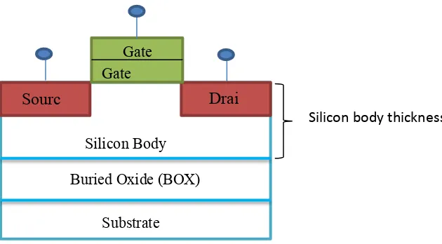
2.4Silicon Body Thickness
Figure 2.4: Silicon body thickness as manipulated parameter in this project
From the figure 2.4.1, it shows that the source and drain are part of silicon body thickness. If any changes regarding silicon body will affect the source and drain region. As mentioned bulk MOSFET already scaled down the thickness but control of short channel effect is become more difficult and it also leading to increase of sub-threshold leakage current. This happen because source and drain influence over the channel potential become significant relative to the gate control [8].
By using ultra-thin body SOI the scalability of MOS device has been improved well. These due to points in the silicon channel are close enough to have a good control thus eliminating the sub-surface leakage currents. Even though, the SOI MOSFET is allowed the scalability of the thickness, the problem still arises when the thickness is far shrink [8]. Besides that, the impact of scaling down the thickness may lead to negative threshold voltage which is not described for device [10].
Gate Gate oxide
Sourc Drai
Substrate Buried Oxide (BOX)
Silicon Body
8
2.5SOI Scaling Effect
As the devices are scaled down, it is more difficult to achieve a scaled transistor with high performance [19]. Even though they can reduce a short channel effect (SCE), leakage current and maintain good scaling capability. SOI transistor still has its own deficiency as it is being shrinking down to nano scale device [20].
2.5.1 Threshold voltage
Referring the PIDS table of ITRS, it shows that SOI device is attracted considerable attention as potential alternative substrate for low power device application. Since the reduction of size, the power supply is also being reduced accompanied by the threshold voltage reduction. However, the lower limit of the threshold voltage is set by the amount of the off-state leakage current that can be tolerated [12]. As for the future invention, controlling the threshold voltage has become more important.
Several factors are uses to control the threshold voltage one is the channel doping. The channel doping will affect the Fermi potential directly with the channel doping increases. With the channel doping increase different threshold voltage can be achieve by adjusting the channel doping [12]. Gate oxide thickness is one of the factors as in increase the gate oxide capacitance is decrease which means the gate has less control to the channel and threshold voltage increase [12].
![Figure 2.3: Challenge in Chips Development [17]](https://thumb-ap.123doks.com/thumbv2/123dok/499600.56008/22.595.193.495.215.373/figure-challenge-in-chips-development.webp)