ICSE2004Proc.2004, Kuala Lumpur,Malaysia
Optical Waveguide Coupler Fabrication Based On Time
Variation Ion-Exchange
Technique
KokSwee
Leong'
andSahbudinShaari2Member, IEEE,Member, SPIEiFaculty of Electronics and Computer Engineering, Kolej Universiti Teknikal KebangsaanMalaysia,
75450 AyerKeroh, Melaka,
MALAYSIA
2Photonics
TechnologyLaboratory,Instituteof Micro-Engineeringand Nanoelectronics UniversitiKebangsaanMalaysia,
43600UKMBangi,Selangor,MALAYSIA Abstract - Optical power transfer in a planar
waveguide directional coupler is dependent on the geometry and refractive indices of the two
waveguides. A method for fabricating optical
directional couplers using ion-exchange Ag+/K+/Ca+ processes is presented, where the timeofion-exchange process is used to control the ratio of output power at the two output portsat afixedtemperatureof
3000C.
As far as the device geometry is still in single-mode regime, this method eliminates the need forhigh-resolution lithography for producing
exactgeometry ofthedevice.
1.INTRODUCTION
Directional couplers are usedto divide the guided light at almost any desired ratio. The main draw back of this device which is based on the field coupling between closed waveguides is their high sensitivity to the fabrication process and device geometry, especially the spacing of the waveguides in the coupling region[1]. Due tothis fact access to high resolution lithography is inevitable for successful fabrication of these devices basedonconventional designs.
Optical planar and channel waveguides fabrication using ion-exchange process is very
common due to low cost and simple technique. The process involves theexchange of sodium ions originally in the glass with other alkali ions of largerpolarizability.
In
this
study,
5samples
of buried
waveguides
werefabricated
using
thermal ion
exchange
process, immersed in molten
mixture of
AgNO3,
KNO3
andNaNO3,
atfixed
temperature of
3000C.
Asthe ion
exchange
timeincreases,
theembedded
graded index waveguide formed by the
diffusion of silver ions is getting deeper and
wider. When
the two waveguides in the
coupling region become closer, the coupling
becomes
moreeasy and
faster, and this allows
the power ratio at output ports to vary. As the
time is
kept longer, larger size of the channel
waveguides
areobtained and effectively
reducing
the spacing.This
effectively changes
the
coupling coefficients between the
twowaveguides
and
eventually their splitting
ratio.
Thereforethis method offers a simple way of getting directional couplers with different output
or coupling ratio by using only a single set of lithography photomask.
II.DIRECTIONAL COUPLER DESIGN
A directional coupler is usually formed by
two identical parallel dielectric waveguides separated fromeach otherby a gap on the order of
awavelength. Consider whentwo waveguides are far enough from each other, two normal modes propagate independently on each waveguide with propagation constants
Pa
andPb
, and the fielddistributionsare
ya
and Ybrespectively. When the separation of the waveguides is reduced, the two waveguide fields interact with each other and this allows the exchange of energy. Coupled mode theory can be used as a method to analyze this behavior [2]. When the separation decreases the coupling between the two waveguides become easier and the energy periodically exchanges along the coupling region. At a certain length L, the maximum transfer of power from one waveguidetoanother will takeplace.For asimpleICSE2004 Proc. 2004, Kuala Lumpur, Malaysia
structure of two identical coupled waveguides, L isgiven by:
where,
L=
g/2fi#
/A
=VK
+A2
;Af=
a
A;
and2
K =
CJY*VYbA6dxCdy
Theschematic of thedesigned couplersare shown in Fig.1 Each ofthem consists of two identical waveguides with width 5 ,um. The design differenceis on its
separation
parameter; onewith 3 pmand the other is 5jim.
III.ION-EXCHANGE
Under certain conditions, it is possible to replacesome of the network modifier ions of glass by others with the same valence and chemical properties. In the so called exchanged region, thus it modifies the glass property. The new ions have different
polarizabilities,
sizes, and mobilities and thus increasingtherefractive index inselectedareasofglass substrate.By exposing the glass surface to the melt nitrates solution, the
Ag3+
ion is diffused into the glass andexchanges with Na+ ions. This is called thermal ion exchange process, where the introduction of the ions is diffusion driven. In ourworkamixtureofNaNO3, KNO3, and
AgNO3
at aratio of 50:50:1 mole % are used. The
melting
point is at
2200C
and the exchange process is at2500C,
the maximum obtainable refractive index contrast is 0.078 (at thesurface)[3,4,5].
V. EXPERIMENTALAND SIMULATIONRESULTS
The ion exchange process was done on
Corning glass with refractive index of
1.515,
and the surface index difference of 0.078 wasobtained. Figure 2 shows the
waveguide
depth
increases with time. It should be noted that while the ion diffuses
perpendicular
to the mask opening, italso diffuseslaterally.
Five samples are fabricated based onthe two different designs.
Sample
1 and 2 have the waveguideseparation
of 3 jim.Exchange
timesfor these samples are I minute and 5
minutes
respectively. Whereas samples3,
4, and 5 have the separationof 5gm,
with the exchange timeof 1 minute, 5 minutes, and 8 minutes respectively. The width allwaveguides isfixed at 5 ,um, andthe
interaction orcouplinglength is 2000
gm.
25mm
Fig. 1 Schematic diagram of two directional couplers design.
4
SW 3
,2-1 ~~3 5 7
ExchangeTime(Minutes) Fig.2Waveguide depthincreasesasionexchange
timeincreases.
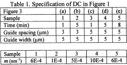
Table I summaries the
specification
of the [image:2.600.328.535.357.502.2]twodirectional
couplers.
Theoutput
ratio ofboth channelsforsample
1, 2,
3, 4,
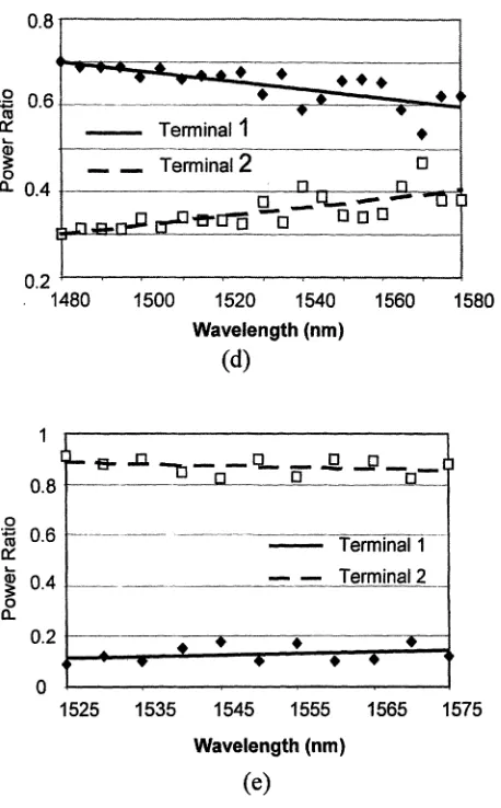
and 5 areshown inFig.
3a,3b, 3c, 3d,
and 3erespectively.
Table 1.
Specifica
tionof DC inFiguLre
IFigure
3(a(c(d(eSample 1 2 3 4 5
Time
(min)
_1
5 1 5 8Guidespacing (pm) 3 3 5 5 5 Guide width
(pLm)
5 ___5 5 5Sample
1 2 3 4 5m(nm-1) 6E-4 1E-4 5E-4 1OE-4 6E-4
The power transfer between
the two armschanges
with thewavelength
and ismeasured
[image:2.600.331.546.599.709.2]ICSE2004 Proc. 2004, Kuala Lumpur,Malaysia
by
the slope m of
thegraph
foreachsample.
Itis
difficult
to discuss and
draw
the
relationship of the slope
obtained relatedwith
the
device design data.
As theion
exchange
time is made longer, the spacing in the
coupling region becomes smaller and at the
same
time the depth of the embedded guide is
deeper. The variation of the width and the
depth of the waveguides will changes the
coupling behavior
between the twoguides.
Figures 3(a)
to3(e)
show
howthe power
ratios between the
twooutput
ports change
with
the
wavelength
for all five
samples
respectively.
VI. CONCLUSIONS
Time for ion exchange process plays very important role where we have shown experimentally that the coupling behavior in directional couplers changes dramatically. By fabricating many more samples with various parametersamore cleartrendcanbeobservedand may beasome conclusions canbesuggested. This may help to determine the exact manufacturing steps process if ion-exchange is adopted as the fabrication method. However from this work we
discover that a number of planar waveguide directional couplers with different coupling ratios
can be made from a single design only, ie. by allowing different time duration during the fabrication.
[5] Stewart. Laybourn, "Optical Waveguide from Dilute Silver Nitrate Melts,"IEEE J.QuantumElec.,Vol.
QE-14, 1978.
0.7
0 (U
0~
0.3 -1480
0 (U
co
I-U).:
0
1500 1520 1540 1560 1580
Wavelength(nm)
(a)
0.7
-0.6 . I mT
Oa
-IJ TerminalTerminal 2
AA5
Terminal 10-4 I_
_ V.,w
0.3
0.2
1480 1500 1520 1540 1560 1580 Wavelength (nm)
(b)
ACKNOWLEDGMENT 1
This work issupported by MalaysianGovernment research grant IRPA 020202T001 for atop down project on the development of WDM-FTTH
system.
REFERENCES
0.8
_ 0.6
2)
0.40
=0.6
0.2 [1] Hamid Reza Azarinia, "Optical Coupler Fabrication
BasedOnBurried Field-Assited Ion-Exchange Method", IEEE, ISIE'99, Bled, Slovenia,1999.
[2] H.Nishihara, M.Haruna,T. Subara, Optical Integrated Circuits, Newyork: McGraww-Hill, 1993"
[31 S.I. Najafi, "Optical Behavior of K+ Exchange Glass
Waveguides. Appl. Opt., Vol. 27, 1988.
[4] Janet L., Jacket, "Glass Waveguide Made Using Low
Melting Point Nitrate Mixtures". Appl. Opt., Vol. 27
No. 3, 1988.
0
1480 1500 1520 1540 1560 Wavelength (nm)
(c)
0-7803-8658-2/04/$20.00(c)2004 IEEE
--qp- V4
aA^ A A* I
lwlw w
Terminal I
- Terminal.
158C
n
,~~~~~~~~~~~~~~~~~~~~~
na
rm
rro-"'
um
tro-a
&V EI-0tru-MICSE2004 Proc. 2004, Kuala Lumpur, Malaysia
0.82
°X0.6 0
06-
TmTerrninal
1aC 04 - _ nTerminal2 °
0
a- 0.4 n
0.2 0.2V . --- T ---, --.
1480 1500 1520 1540 1560 1580 Wavelength (nm)
(d)
0.8 13 a aa
to Terminal 1
xlO0n.4 (-)
Sample3,5x0nm,(d)Sample4,1Terminal
20.2 X
1525 1535 1545 1555 1565 1575 Wavelength (nm)
(e)
Fig. 3 Outputpower ratiodependenceonwavelengthatboth channelof the five fabricatedsamplescorresponding
towavelengthof 1480 nlmto1580nm.Thegradientforthegraphin(a)Sample 1,6.0
x104X
nm-',
(b)Sample2, 1x
10-4nm-1,
(c)Sample3,5x104nm-',
(d)Sample4, 1x10⁻³nm-1,
(e) Sample5,6xI10-4nm-1.
[image:4.600.121.350.113.482.2]