i
TWO STAGE AMPLIFIER DESIGN FOR UHF APPLICATION (460MHZ-530MHZ)
NURUL AFIQAH BINTI AZIZ
This Report is Submitted in Partial Fulfillment of Requirement for the Bachelor Degree of Electronic Engineering (Telecommunication Electronic) with
honours
Faculty of Electronic and Computer Engineering Universiti Teknikal Malaysia Melaka
v
vi
ACKNOWLEDGEMENT
First and foremost, I would like to express my sincere gratitude to my supervisor Ms. Fatimah for the continuous support in order to finish this project. Without her assistance and dedicated involvement in every step throughout the process, this project would have never been accomplished. I would like to thank you very much for your support and understanding over these past two semesters.
I would also like to show gratitude to my co supervisor, Mr. Harris who is always helpful and patient when guiding me. He has given me a lot of ideas and suggestions in order to design two stage power amplifier which having such an excellent performance. I feel lucky and grateful upon his guidance and kindness in helping me into this project.
Next, I would like to thank to my classmate for taught me a lot on the basic of using ADS software. I really appreciate all the hard work of my classmate to make me understand steps of using and designing power amplifier in ADS.
Most importantly, none of this could have happened without my family. My mother, who offered her encouragement through phone calls once every week. She motivated me from time to time to ensure that I am on the right track in finishing this project.
vii
ABSTRACT
viii
ABSTRAK
ix
TABLE OF CONTENTS
ACKNOWLEDGEMENT ... VI ABSTRACT ... VII ABSTRAK ... VIII TABLE OF CONTENTS ... IX LIST OF TABLES ... XII LIST OF FIGURES ... XIII LIST OF ABBREVIATIONS ... XV LIST OF APPENDICES ... XVI CHAPTER I
INTRODUCTION
1.1 Project background ... 1
1.2 Problem statement... 2
1.3 Objective ... 2
1.4 Scope of work ... 2
1.5 Thesis outline ... 3
CHAPTER II LITERATURE REVIEW 2.1 Introduction ... 4
2.2 Design consideration... 4
2.3 Two stage amplifier topologies... 5
2.3.1 Feedback amplifier ... 5
x
2.4 Scattering parameter ... 8
2.5 RF transistor characteristic ... 10
2.6 Two port power gain ... 12
2.6.1 Power gain ... 12
2.6.2 Available power gain ... 12
2.6.3 Transducer power gain ... 12
2.7 Noise figure... 13
2.8 Stability ... 13
2.9 DC biasing ... 14
2.10 Matching network ... 17
2.10.1 Input matching ... 18
2.10.2 Output matching ... 18
CHAPTER III DESIGN METHODOLOGY 3.1 Introduction ... 19
3.2 Methodology ... 19
3.3 Design specification ... 23
3.4 Stability checking ... 24
3.5 DC biasing ... 25
3.6 Matching network ... 25
3.7 Two port power gain ... 27
xi
CHAPTER IV
RESULT AND ANALYSIS
4.1 Introduction ... 29
4.2 Stability analysis ... 29
4.3 DC biasing ... 33
4.4 Two port power gain ... 35
4.5 Noise figure... 39
4.6 Maximum gain (conjugate matching) ... 39
4.7 Matching network ... 42
4.7.1 Input matching ... 42
4.7.2 Output matching ... 43
4.8 Microstrip line implementation ... 44
4.9 Simulation result of two stage conventional amplifier ... 48
4.9.1 Before optimization ... 48
4.9.2 After optimization ... 49
4.10 Balanced amplifier ... 51
4.11 Feedback amplifier ... 53
4.12 Analysis summary ... 55
CHAPTER V CONCLUSION AND FUTURE WORK 5.1 Conclusion ... 56
5.2 Future work ... 57
REFERENCES ... 58
xii
LIST OF TABLES
Table 2.1 Performance characteristics of RF transistor ... 11
Table 2.2 BJT bias configuration ... 15
Table 3.1 Design specification of two stage amplifiers ... 23
Table 4.1 S-parameter data in ADS model ... 29
Table 4.2 Comparison the stability factor over frequency range ... 33
Table 4.3 Comparison between the calculation and simulation result at frequency 500MHz ... 39
xiii
LIST OF FIGURES
Figure 2.1 Block diagram model of feedback amplifier ... 6
Figure 2.2 Two stage circuit of feedback amplifier ... 6
Figure 2.3 Principle of the balanced amplifier ... 7
Figure 2.4 Two port S-parameters ... 8
Figure 2.5 Matching for a transistor amplifier ... 17
Figure 3.1 Design flow of the two stage amplifiers ... 23
Figure 3.2 DC bias setup for the transistor ... 25
Figure 3.3 Different region of L and C matching network. ... 26
Figure 3.4 Art of designing matching network ... 27
Figure 4.1 Stability analysis in ADS ... 32
Figure 4.2 Stability result of BFR380F ... 32
Figure 4.3 DC bias setup for the transistor ... 33
Figure 4.4 BJT curve for the transistor ... 33
Figure 4.5 Biasing circuit ... 34
Figure 4.6 Biasing circuit of BFR380-F ... 34
Figure 4.7 ADS simulation of the s2p model ... 36
Figure 4.8 Result of the source reflection coefficient, for the minimum noise figure ... 36
Figure 4.9 Gain from ideal biasing circuit of BFR380F ... 38
Figure 4.10 Noise figure from the biasing circuit of BFR380F ... 39
Figure 4.11 Input matching with series capacitor ... 42
Figure 4.12 Input matching with shunt inductor ... 42
Figure 4.13 Schematic of input matching ... 43
xiv
Figure 4.15 Output matching with series capacitor ... 43
Figure 4.16 Schematic of output matching ... 44
Figure 4.17 Schematic for the input and output matching ... 47
Figure 4.18 Schematic for DC biasing ... 47
Figure 4.19 Schematic of two stage amplifier before optimization ... 48
Figure 4.20 Stability factor before optimization ... 48
Figure 4.21 S-parameter before optimization ... 49
Figure 4.22 Noise figure before optimization ... 49
Figure 4.23 Schematic of two stage amplifier after optimization ... 49
Figure 4.24 Stability factor after optimization ... 50
Figure 4.25 S-parameter after optimization ... 50
Figure 4.26 Noise figure after optimization ... 50
Figure 4.27 Schematic of two stage balanced amplifier ... 51
Figure 4.28 Stability factor of balanced amplifier ... 52
Figure 4.29 S-parameter of balanced amplifier... 52
Figure 4.30 Noise figure of balanced amplifier ... 53
Figure 4.31 Schematic of two stage feedback amplifier ... 53
Figure 4.32 Stability factor of feedback amplifier ... 54
Figure 4.33 S-parameter of feedback amplifier ... 54
xv
LIST OF ABBREVIATIONS
ADS – Advance Design System BJT – Bipolar Junction Transistor FET – Field-Effect Transistor MAG – Maximum Available Gain NF – Noise Figure
RF – Radio frequency
xvi
LIST OF APPENDICES
APPENDIX TITLE PAGE
A Smith chart of input matching 60
B Smith chart of output matching 61
1
CHAPTER I
INTRODUCTION
1.
1.1 Project background
2
1.2 Problem statement
RF power amplifiers play an important role in modern telecommunications, where opposite design goals make the performance optimization of amplifier very difficult. Two stage amplifiers design is challenging as it required simultaneously to achieve the high gain, low noise figure and also good matching. However it is very hard for the conventional amplifier to meet these specifications. So it has many solutions to solve that problem and one of the solutions is by using multistage design.
1.3 Objective
In this project, different topologies of the two stage amplifiers design are proposed to solve the problem faced by the conventional amplifier and also to further improve on the performance of the amplifier. Balanced, and feedback of the two stage amplifiers are designed and compared. This design also can be operate over frequency range of 460MHz-530MHz
1.4 Scope of work
The scope for this project can be divided into two parts which are: a) Literature review
The study of the RF fundamental and characteristics of the two stage amplifiers especially on the high gain, noise figure, stability which must be taken into consideration in two stage amplifiers
b) Design and simulation
3
1.5 Thesis outline
The thesis is divided into five chapters which covers the complete design process of the two stage amplifiers design. Chapter 1 includes the brief introduction of the project where the problem statement, objective and scope of works are mentioned clearly in this chapter.
Chapter 2 is the literature review which discusses the topic on the RF fundamental such as scattering parameter, stability, high gain, noise figure and others that related on to the two stage amplifiers. There also discuss about the information on the different two stage amplifiers topologies namely balanced and feedback amplifier.
Chapter 3 is about on the design methodology which describe the design process of the two stage amplifiers which is include the selection transistor, checking the stability, design the input and output matching and others steps.
Chapter 4 is mainly on the result and analysis. This chapter will includes the manual calculation and also simulation result by different types of topologies of the two stage amplifiers. The simulation results are compared and analyzed by each topologies.
4
CHAPTER II
LITERATURE REVIEW
2.
2.1 Introduction
Two stage amplifiers is one type of the multistage amplifier. In multistage amplifiers, the low noise stage should be first and the highest intercept stage should be last. If the overall gain control is required, the gain of the first stage is usually controlled to avoid overload under strong signal conditions [2]. It frequently used in transmitter driver circuit. In many applications, the control of the stage gain by changing its bias current is unacceptable, because to obtain lower gain so a lower bias current is required. The action by lower the intercept point is undesirable because of the lower gain is required exactly when the input signal levels are high. With the high input signal levels, it could to operate at a higher bias condition to avoid distortion. The total amount of the gain that is achievable with the multistage is ultimately limited by the isolation between the output and input. When the overall gain is greater than the isolation, the oscillation may result.
2.2 Design consideration
5
be firstly considered in order to determine the biasing point of the and that will produce optimal performance.
Another important parameter that needs to be considered in designing power amplifier is stability checking. Unconditional stability of the circuit has to be achieved at the operating frequency so that the amplifier will not oscillate and become unstable. The scattering coefficients of the transistor were determined. The input circuit should match to the source while the output circuit should match to the load in order to deliver maximum power to the load. The input and output matching is the last step in designing two stage amplifiers.
2.3 Two stage amplifier topologies
The importance goal in designing two stage amplifiers is to achieve a high gain of the amplifier, minimize the noise figure and also producing a stability of 50Ω input impedance.
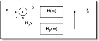
2.3.1 Feedback amplifier
6
Figure 2.1 Block diagram model of feedback amplifier
Feedback amplifier gives the better performance including increase the stability, reduces distortion in the amplifier, increase the bandwidth of the amplifier and it is easier to achieve the desired input and output impedances.
Figure 2.2 Two stage circuit of feedback amplifier
7
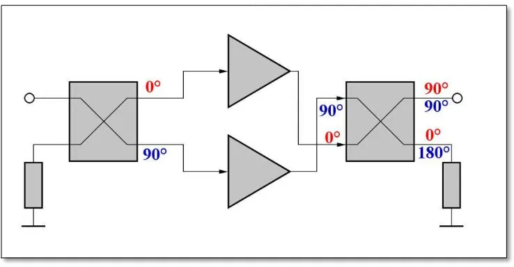
2.3.2 Balanced amplifier
Balanced amplifier is very important in many high frequency system because it is exhibits high bandwidth, have flat gain, and also good standing wave ratio at the input and at the output. A balanced amplifier provides a 3dB higher linearity as compared to a single power amplifier by employing 3dB Quadrature Hybrid coupler. Most of the power amplifier designs are based on non-linear large signal models.
Balanced amplifier has two amplifying devices that are run in quadrature. That is, they are operating 90 degrees apart in transmission phase. A quadrature coupler or splitter on the input phase-shifts the two signals 90 degrees at the amplifier inputs, then a second quadrature coupler on the output "un-phase-shifts" the signals at the amplifier outputs so they combine in phase.
Figure 2.3 Principle of the balanced amplifier
8
input. For near-identical devices they subtract from each other when they combine, so they combine to zero volts, and ultimately a great input match. A similar thing happens at the output. The bottom line is this: you can combine stuff with poor reflection coefficients and the amplifier end up matched closely to fifty ohms, so long as the devices are nearly matched in reflection coefficients.
Usually balanced amplifier has excellent input and output return loss. If they are presented with a bad match on the output, the bad match is seen by both amplifiers, but at phase angles differencing by 180 degrees. The load that terminates the isolated port on the output can see sizable heat dissipation if the phases of the two amplifiers (or their amplitudes) are not exactly the same. The use of balanced amplifiers at millimeter wave is quite common.
2.4 Scattering parameter
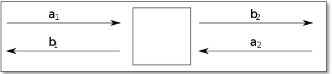
Scattering parameter or S-parameters describe as the electrical behavior of linear network when undergoing various steady state stimuli by electrical signal. It is very useful for electrical engineering, electronics engineering and especially for microwave engineering.
S-parameters are important in microwave design as they are relatively easy to obtain at high frequencies. It can be measured directly using vector network analysis. It is usually related to familiar measurements like gain, return loss, reflection coefficient and so on [1]. In addition, S-parameter file also easily can be import by using electronic simulation tools like ADS. In two stage amplifier design, S parameters will provide necessary values to do analysis on the stability and gain