IEEE PEDS 2005
High-Frequency Transformer-Link
Inverter
with
Regenerative Snubber
L. S.
Toh, Student Member, IEEE, Z. Salam, Member, IEEE and M.Z. Ramli
Power Electronicsand Drives Group, Department of EnergyConversion, Facultyof ElectricalEngineering, Universiti Teknologi Malaysia,
81310 UTMSkudai, Johor,Malaysia.
leong_soon_toh(ieee.org,
zainals(fke.utm.my,
gogainet(time.net.my
Abstract-This work proposes a bidirectional high-frequency link High-frequency link inverters are now commonly used in
inverter using center-tapped high-frequency transformer. The uninterruptible power supply and renewable energy source
topology also incorporates a regenerative snubber to clamp the systems. In these applications, the types of loads connected to
high voltage spikes due to the leakage inductance of the the inverter are rather uncertain. Nonlinear loads such as transformer. The closed-loop control method used is Deadbeat rectifier in computer systems could cause intense distortion in control, which provides fast response and low harmonic the output current and voltage waveform. It is desirable that the distortion, even under nonlinear loads. A lkVA prototype inverter be able to maintain a sinusoidal output voltage
inverter is built and the workability of the system is
waveform
over allloading
conditions. This canonly
beexperimentally
verified.achieved
by employing closed-loop control. Commonly, theKeywords-Bidirectional; Deadbeat control; HF transformer; Proportional-Integral-Derivative (PID) control method [4], [5] Inverter;Pulse width
modulation.
is used for closed-loop regulation of inverters. Although digital controllers using microprocessors and Digital Signal Processors (DSPs) have become more prevalent over analog I. INTRODUCTION based controllers, the discrete PID control is still adopted. High-frequency link inverter is frequently used in dc/ac Despite its simple structure, the PID controller is known to power conversion in which compactness and light-weight are have a slow response.of importantconsiderations. For this type of inverter, the high- In this paper,we propose an
improvement
to ourprevious frequency transformer is used, resulting in a significantwork.
Weintroduce
aregenerative
snubber network for the reduction in size and weight compared to the conventionalactive
rectifier thateffectivel
reduces
thespike
to
aye low 50Hz transformer inverter. However, it is well known thatyalue
Oigtothe
essct
atureduce
the ide case)ow
hig-frquncylin ivererhasthe problem of voltage spike at value. Owing to the lossless nature (in the ideal case) of thehigh-frequency
linkinverteris
the pr
espike
atsnubber,
the
energy
contained
inthe
voltage
spike
is
pumped
the transformersecondary.
This is due to the presence ofback to the
main power circuit. Besides,
we also
propose
a
fast
leakage
inductance at thetransformer
secondary.
When theDeadbeat controller for
the
inverter.
As
such,
the
system can
cur-rent
through
the switch is tumed off veryquickly,
the di/dt handle critical loads suchasrectifier load and triac load. isveryhigh,
resultinginhigh voltage spike to appear across theswitch. If notproperly controlled, thespikes may result in the This paper is organized as follows: Section II describesthe
switchdestruction. circuit configuration of the proposed inverter andregenerative
In our previous paper
[1],
we have described ahigh-
snubbernetwork,
and thestructure
of theDeadbeat controller.frequency link inverter using the center-tapped transformer. Section III shows the hardware construction of the system. We have shown that this circuit utilizes fewer switches
Section
IV depicts theexperimental
results and discussions.compared
tothetopologies proposed by [2]
and[3].
HoweverSection
V concludes theentire
work. usingthe center-tapped transformer has one major drawback:the voltage across the switch at the transformer secondary is
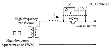
double relative to the noncenter-tapped type. As the voltage R, RCD snubber
stress acrossthe switch isalready high,additional voltage spike D,
',
canmake thepower switch vulnerable. The normal method to ---
----dampen the spike is to use aRCD snubber network, as shown High-frequency
in Fig. 1. However, for adequate spike suppression, the fr5nsfonT1r T
Power
switchrequiredsnubber capacitor, Cs can be quite large. Consequently
high
discharge
energy will bedissipated
inthesnubberresistor,
Rswhen the switchtumsbackon.This mandates for the use of High-frequency highpower
R5,
whichcan lead tofiurther
loss ofthe inverter's square wave orPVWMAefficiency.
[image:1.588.308.541.565.672.2]II. SYSTEM DESCRIPTION
A. Power Circuit
VHF
iLOLL]+HIrLUflUB]%I
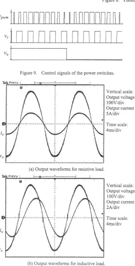
Theproposed bidirectional high-frequencylink inverter is shown in Fig. 2. The timing diagram for the key waveforms of the power stage is illustrated in Fig. 3. At the first stage, the
high-frequency
PWMbridge
converts the dcvoltage
toa50Hz
Vpwm2rec1
modulated Sinusoidal Pulse Width Modulation
(SPWM)
high-
_frequency ac voltage. Then,
this
voltageis
isolated and stepped-up using a center-tapped high-frequency r-ansformer.In the next stage, the high-frequency SPWM waveform is Vrect rectified
using
acenter-tapped
active rectifier. The activeI
rectifier, which consists of power switches and anti-parallel diodes, enables bidirectionalpowerflow.Fortransfer ofpower from the source, the diodes are utilised. For reverse power
flow, the power switches S3 and S3 are turned on. The vo
rectifiedPWMwaveformis thenlow-passfilteredtoobtain the rectified fundamental component. Finally, using a polarity-reversing bridge, the second half of the rectified sinusoidal voltage waveform is unfolded at zero-crossing, and the
sinusoidal output voltage waveform is obtained. By using Figure3. Keywavefomsatdifferentstagesofthedc/acconversion.
center-tapped rectifier circuit, the number of bidirectional When the gate
signal
isapplied
to any of the rectifier's switches is reduced. Furthermore thepolarity-reversingbridgeswitch,
voltage
spike
will
appear on
theadjacent
(off)
switch.
utilizesonly
line-frequency (50Hz)
switches. This can beattributed
to the energy stored in the leakage inductance of the transformer that appears as voltage spike with B. Regenerative Snubber Network a sudden currentturn-off. Assume the snubber diode(D3)
andDue tothe leakageinductance and high di/dt, appreciable snubber switch (S3) are ideal, the voltage across snubber amplitudeofvoltagespike will be developed across the active capacitor
(CQ)
without spike is v1. When spike occurs,vp,m_,HF
rectifier switches during switching transitions. The normal increases, thus causingD,
to be forward biased and chargesCi.
practice to suppress this voltage spike is to place a RCD The capacitor
C,
dampens the voltage spike by reducing its snubber across the switches. For effective damping, a di/dt. The charging process that takes place from t1 to t2causes relatively large snubber capacitor and a high power resistor is the capacitor voltagev,s
to rise. Whenv,s
equals v2, i.e. when required. As aresult, efficiencyof the inverter will be reduced. the capacitor voltage equals to Vpwm HHF, the charging process Inthis work, we propose a regenerative snubber network as stops. Snubber diodeD,
is reverse biased and C5 starts to denotedby the dashed box in Fig. 2. The aimof the snubber discharge its energy into the power circuit viaS,.
The circuit is to reduce the voltage spike across the active discharging process continues until end of the PWM pulse. rectifier's switches(S3and S3) to a safe level. It comprises of When the PWM pulse has ended, S3 is turnedoff,
and thea snubber
capacitor,
snubber diode and a transistor. Fig. 4 discharging process stops. Voltage vc, is maintain at its details the snubber network and its associatedtiming diagram. equilibriumlevel(v,)until the next charging process occurs.R egeneraive
H
bglfreiguencsy
Active srbber circtitPolaity-reversing
High-Frequency
rectifier
Vwm creL
bridge
*
~~~~~~~~~4
S5T~~3 ::Ds
Ss
Ml
-H
V dc~ ~ ~ ~ *
1
se
-
i
Cs
S4
SC
[image:2.588.323.533.38.238.2]Vpwm l
+VL
£S3
Vpwm2:t
V2
-,.-..
Figure
4.
C.rcuit
ofDregenerative
snubber
networ andtheassocatmChirgdgagrre
aC.Vpwm DF C F 6 s t r
d
netwCs
Vc,
is ut
provides fast dynamicresponse[6],[7].In Deadbeatcontrol, discretizatio,theclosed-lpatransefunturrent
Ls vc,
Vl
+VI,
Y
3_
Vwretv3-::C::Figure4. Circuitofregenerativesnubbernetwork and theassociatedtirning
diagra..
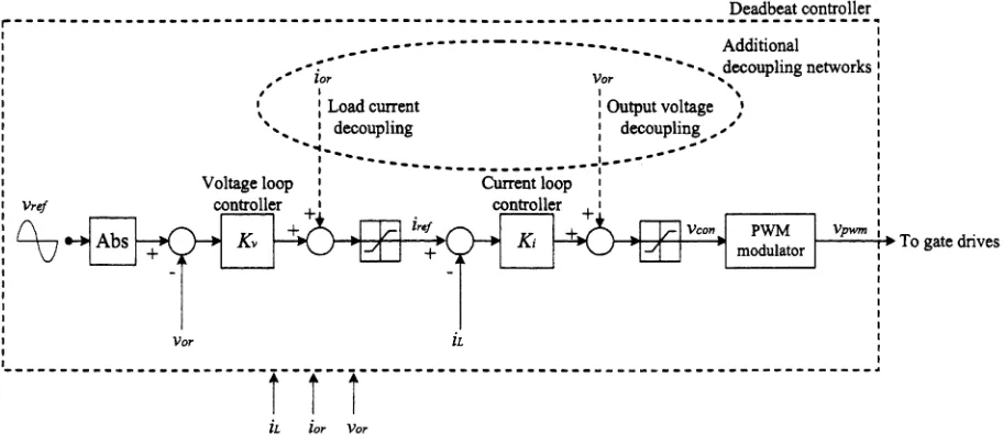
C. Deadbeat Controller
decoupling
Fig.
6 shows thenetworkcurrentis usedloop
tocontroller. The outputvoltage
compensate the disturbances Deadbeat control is a discrete-time controltechnique
that causedby
the outputvoltage.
With f(rtlersimplification
andprovides
fastdynamic
response[6], [7].
In Deadbeatcontrol,
discretization,
theclosed-loop
transfer function of the currentany nonzre rror vectorwill be driven to zero in at most n
loop
isobtainedasampling periods,
where n is the order of theclosed-loop
system
[8].
Inthiswork,amultirateDeadbeatcontroller is usedfor
closed-loop
regulation
ofthehigh-frequency
link inverter. Ki
Ti
Az-i
Referring
toFig.
2, it is assumed that the Vdb is constant. iL L)
The
switching frequency
is considered to behigh enough
C z 3compared
to themodulating
frequency.
Thehigh-frequency
rf K, i lz- +1transforrner is assumed to be
operating
in the linear area. LTherefore,
the PWMbridge
and the transformner can bemodeled as constant
gains.
Thepolarity-reversing
bridge
is To achieve Deadbeat response, whereiL
=zli,,f
,the
current only operated at 50Hz, thus can beignored.
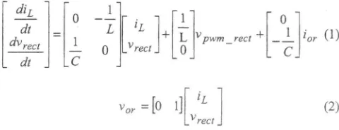
With theseassumptions, the dynamicsof thesystemcanbesimplifiedtoa loopgain, K, isdesignedas: LClow-pass filter connected to the load.
Choosing
Vpwmrect asthe input voltage of the system, filter inductor current iL and
filter
capacitor voltage
VreC,
as the statevariables,
the state- Ki=(4)
space modelof thesystem isderived:
Ti
Fig.
7 shows thevoltage
loop
controller. The load currentdiL
0--I
1 F 0decoupling
network is used tocompensate
the disturbancesdt
T
ViL
4.Vpwm
L rect+
.
Ir
(1)
induced by the load current.This
improves the robustness
ofdvrect
- lvrect
L L the system towards load variations, allowing different types ofdt -C loads to be connected. The design procedure of the voltage
loop
controller is similar to the currentloop
controller. TheV
iL
- closed-looptransfer function of the voltage loop is:Vor =
[0
1](2)
_vreci
I
wherevoristherectified sinusoidal outputvoltage.
Co
=vor
v_(T
C_
)The controller isdesigned basedonthe state-spacemodel,as C ( =-=f
r-
(5)shown in Fig. 5. It consists ofcurrent and
voltage
loop
with Cdecoupling
networks. Thedecoupling
networks are used to [image:3.588.349.501.346.408.2] [image:3.588.45.285.506.598.2]Deadbeatcontroller
r---__ --- Deadbeat
controller.____
______-- - ~ ~~~~~~~~~---_____ Additional
'bor Vor ' decoupling
networks
I
8 I ~ ~ ~~~~~~~~~~~~~~~~~~~~~I %
Loadcurrent Output voltage ;
decoupling decoupling ,,'
Voltage loop Currentloop
Vref controller + controller +
Abs K~~~~~~ + K
~~iefVcoi,
+ PWM Vpwm1V
v X++ , modulator Togatedrives
Vor iL
iL ior Vor
Figure5. Deadbeatcontroller for the high-frequency link inverter.
Outputvoltage
Plant
ETD59ferrite
core. The active rectifier's switch is built usingdecouplMng --- - --- -
----the IRG4PH40K IGBT and STTA1212D ultrafast high voltage Unknown-load diode. These power switches can withstand 1200V, thus suitable to be used at the center-tapped active rectifier. The polarity-reversing bridge is constructed using the 1 11+ I Vol, IRG4PC40FD IGBT. Since almostall the surge
voltages
have+ Xi sL
:sCi
been dampened before entering the polarity-reversing bridge,--- the chosenpower switches are only rated at600V. Using low
voltage
IGBT,
the forward conduction losses can be minimized. The snubber capacitor is chosen tobe2.2pF,
and Figure6. Current loop controller. the snubber switch is an IRF730 MOSFET. Each power transistor is driven by a Hewlett Packard gatedriver
chip,Loadcurrent Unknown load HCPL3120.
decoupling [ ~ 7 I DS1104 DSP board from dSPACE
(64-bit
floating-point
processorwith TMS320F240
SlaveDSP) isused to implement TV7; ++ti7of Inner iL + tt the Deadbeat controller. It is also used to generate the control+ K current
E
_
signals
for the activerectifier, v,
and thepolarity-reversing
loop
bridge,v,.
The controlsignals are shown inFig.9. Hall effect IDO
current sensors, HY1O-P andvoltage sensor, LV25-P are used forfeedback signals sensing. The signal conditioning such as noise filtering and signal amplification are performed in Figure7. Voltage loop controller. software usingtheDS1104DSP.To ensure Deadbeat response of
vor
=z-lVref
the voltage IV. EXPERIMENTAL RESULTSANDDISCUSSIONSloop gain,
K,
isdesignedas:Laboratory experiments
have beencarried
out toverify
theviability
of theproposed
inverter. Thespecifications
of theK = - (6) inverterare asfollows:
* Inputvoltage rangedfrom 130Vto 15OV. * Sinusoidal outputvoltage220to
250Vrm,,
50Hz.III. HARDWARE CONSTRUCTION * Nominaloutput powerof1kW.
[image:4.588.81.537.37.239.2] [image:4.588.44.284.273.503.2]--_DC linkcapacitors
Powerswitches - Regenerativesnubber
and gatedrivers Low-passfilter
Logicgates .._j., Sensors
_| lj_|_ = ; _ High-frequency
transformer
(a)Top view-gate drive andsignalconditioningcircuits (b) Bottom view-power circuit
[image:5.588.67.542.45.149.2]Figure8. Photograph ofthe prototypeinverter.
Fig. 12 shows the active rectifier's switch (S3)
collector-VPWM
acnncnng 1 ucnncn
emitter
voltage (VcE)
before and after insertion of
theregenerative snubber. It can be seen that before the
regenerative
snubberisinserted,
thevoltage
overshootis about VS I { I | X } X {, 40% of the amplitude. After the insertion of the regenerativesnubber, thespikehas beenreducedtoanegligiblevalue.
v_ _ _
_.
Fig.
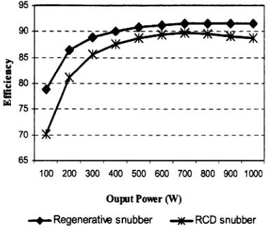
13 compares the inverterefficiency
between theregenerative snubber and the conventional RCD snubber. For
thelatter, the values of Cs and
R,
are chosen to be 2.2nF and Figure 9. Control signalsof thepower switches. 22Q, respectively. The chosen values for the RCD snubberTeKPreVu F n ' 1
components
are ratherconservative; typical
values are muchhigher
than these. From thefigure,
it can be seen that theOutput
voltage
regenerative snubber is able to increase theefficiency
of thelOOV/div inverter by about 5%. A higher value for RCDcomponentswill Outputcurrent make the differenceeven
larger.
1\T
T\
S~~~~~~A/div
Time scale:4ms/div Ha = Verticalscale:
CHla: IOV/div
CH2a: 300V/div
* CH43a: IA/div
\2 \
CH2a
;
L
CH4a:5OV/div
VO o * a . . n 0 . CHlb:300V/div
.. . |,.. . ... .
*CH2b: 600 V/div
(a)Outputwaveformsforresistiveload. 1'. . . CH3b: 600V/div
TekPreXu,l
F n ' I CH3aTimescale:
Vertical scale: IOIls
Outputvoltage CH4a
100OV/div
_____________________Outputcurrent X ___,_______t''Z''':'''''''_'''_'''
2A/div
c-.-~-t.if--
A: +-.- Timescale: CHCHla:vpwm4ms/div CH2a:vpwm_HF
io
J \ u
\
f
~~~~~~~~~~~~~~~~~~~~~~~~CH3a:
iCs
CH2b
,
X
'
CH4a: VC\-i \ : : . CHlb:vpwm rect
V0
* *CH2b: VCEatS3
CH3b L _
CH3b:
VCEat S3(b)Outputwaveforms for inductiveload.
Figure 10. Outputwaveformsforresistive and inductive loads..
Fig. 1 shows the keywaveformsthat depicts the operation Figure11. Keywaveformsofthesnubberoperation. of the regenerative snubber. It can be seen that the snubber
[image:5.588.53.272.163.593.2] [image:5.588.305.547.357.623.2]ff l , X - -, - - 1 : . - - ! - . To TInPreVu
To PreVu [. ... ..._| Vertical scale:
Outputvoltage
IOOV/div
Outputcurrent
5A/div
-~ J.~ I.~-
-J:- I:-- iTime
scale:4ms/div
Vertical scale:200V/div Verticalscale: 200V/div Time scale:5ps/div Time scale:5As/div
[image:6.588.43.280.37.163.2](a) VcEofS3without snubber (b) VcEofS3with snubber vo
Figure 12. VCEatS3beforeandaftertheinsertionof regenerative snubber. ...I..i.._I..I_... _.
95 Figure15.Outputwaveforms forfull-bridgerectifierload.
90
V. CONCLUSION
85 This paper has
described
thehigh-frequency
link inverterwith aregenerative snubber anddigital closed-loop controller.
80
/ To prove the
concept,
a 1kVAprototype
inverter is75
-_
--constructed.
From the experimental results, it was found thatthe snubber network functions aspredicted.Thevoltage spike
70- -acrossthe active rectifier's switch is reducedsignificantly.This
increases the overall efficiency of the inverter. Besides, the 65
0 200 300
400, ,00
600 700.00
900 IWO Deadbeat controller exhibits excellent dynamic response with100 200 300 400 500 600 700 800 900 1000 lowharmonic distortion, even under highly nonlinear loads. It
Ouput
Power (W)is
thus concluded that the proposed inverter issuitable
for widearea of applications, both in stand-alone and grid-connected
[image:6.588.310.535.38.174.2]-+ Regenerative snubber )K RCD snubber configurations.
Figure 13. Efficiency vs output power. REFERENCES
Fig. 14 shows the output voltage and current waveforms [1] M. Z. Ramli, Z. Salam, L. S. Toh and C. L. Nge, "A bidirectional high-understep loadchangefor resistive load. A triac load is used as
frequency
link inverter usingcenter-tapped
transformer,"
IEEE
Proc. of the load. Itcanbe seen thatthe voltage drop can be recoveredPESC'04,
pp.3883-3888,June 2004.quickl,
evenunderlargecurrenttransient.[2]
M. Matsui, M. Nagai, M. Mochizuki and A.Nabae,
"High-frequencyquickly
evenunaer large current translent. linkdc/acconverterwithsuppressed voltage clampcircuitsNaturally
Totest a worse-case loading, the system is connected to a commutatedphase anglecontrol with selfturn-off devices," IEEETrans.
full-bridge
rectifierload,
withacapacitor filter, Cd
andresistive on1996.Industry Applications,vol. IA-32,no.2,pp. 293-300, March/April load, Rd of 470iF and 500Q2 respectively. The steady-state [3] E. Koutroulis, J. Chatzakis, K. Kalaitzakis and N. C. Voulgaris, "Aresult is shown in Fig. 15. It can be seen that the sinusoidal bidirectional, sinusoidal, high-frequencyinverterdesign,"IEE Proc. on
outputvoltageis maintainedalthough the load current is highly Electric Power Applications, vol. 148,no.4,pp.315-321, July 2001.
distorted. [4] N. M. Abdel-Rahim and J. E. Quaicoe, "Analysis and design ofa
multiplefeedback loop control strategy forsingle-phasevoltage-source UPSinverters,"IEEETrans. onPowerElectronics,vol. 11,no. 4, pp.
Ts_==stopI 532-541,July 1996.
. Verticalscale: [5] S. Choudhury, "Implementing triple conversion single-phase on-line
rOutput
voltage UPS using TMS320C240," Application Report SPRAS89A, TexasInstruments,September1999.
Outputcurrent [6] K. P.Gokhale,A. Kawamura and R. G.Hoft,"Deadbeatmicroprocessor X5\-t {SA/div control of PWM inverter for sinusoidaloutput waveformsynthesis,"
IEEETrans. onIndustryApplications, vol.IA-23, no. 5, pp. 901-910,
D4+-i-,*-iS-r1_¢i-iwi-ri_ti-j Time scale: 1987.
Vl \ " / 4ms/divl. [7] S. L. Jung, M. Y. Chang, J. Y. Jyang,L. C. Yeh and Y. Y. Tzou,
"Design and implementation of an FPGA-based control IC for ac-voltage regulation,"IEEETrans. onPowerElectronics,vol. 14, no. 3, pp.522-532, 1999.
vo V \ / \ [8] K.Ogata, Discrete-time control systems, 2nded.,New Jersey:
Prentice-Hall,Inc., 1995.
[image:6.588.66.262.185.353.2] [image:6.588.54.275.510.648.2]