THE DEVELOPMENT OF PEAK CURRENT MODE CONTROL OF BUCK CONVERTER
Farah Atika Binti Ahmad Azam
v
ABSTRACT
vi
ABSTRAK
vii TABLE OF CONTENT
CHAPTER TITLE PAGES
SUPERVISOR APPROVAL i
STUDENT DECLARATION ii
STUDENT DEDICATION iii
ACKNOWLEDGEMENTS iv
ABSTRACT v
ABSTRAK vi
TABLE OF CONTENT vii
LIST OF TABLES x
LIST OF FIGURES xi
LIST OF APPENDICES xiv
CHAPTER 1 INTRODUCTION
1.1 Project Background 1
1.2 Problem Statement 2
1.3 Objectives 3
1.4 Scope 3
1.5 Report Outlines 3
CHAPTER 2 LITERATURE REVIEW
2.1 Theory and Basic Principle 5
viii
2.1.1.1 DC-DC Converter- Buck Converter 7
2.1.1.2 Operation of Buck Converter 8
2.1.1.3 Design of Buck Converter 12
2.1.2 Voltage-Mode Control 14
2.1.3 Current-Mode Control 15
2.1.4 Compensator 19
2.1.4.1 Type II Compensator 19
2.1.4.2 Type III Compensator 23
2.1.4.3 The K-Factor Concept 25
2.2 Previous Problem 26
2.3 Summary of Review 29
CHAPTER 3 DESIGN METHODOLOGY
3.1 Project Activity 30
3.1.1 Flowchart 33
3.2 Simulation 34
3.2.1 Mathematical Modeling 34
3.2.1.1 Buck Converter State Equation 36
3.2.2 Power Stage Design 43
3.3 Simulation Design of Buck Converter Power Stage 46
3.4 Type II Compensator Design Procedure 47
3.5 Simulation Design Peak Current-Mode Control Of 52
Buck Converter
3.6 Simulation Design Voltage-Mode Control Of 54
Buck Converter
CHAPTER 4 RESULT AND DISCUSSION
4.1 Power Stage Buck Converter Result 56
ix
4.3 Closed-Loop Buck Converter: 66
Peak Current-Mode Control Result
4.4 Closed-Loop Buck Converter: 70
Voltage-Mode Control Result
4.5 Discussion Of Buck Converter Simulation Result 74
CHAPTER 5 CONCLUSION AND RECOMMENDATION 76
5.1 Conclusion 76
5.2 Recommendation 78
REFERENCES 79
xi LIST OF FIGURES
CHAPTER TITLE PAGES
CHAPTER 2 LITERATURE REVIEW
Figure 2.1 DC-DC Converter Block Diagram 6
Figure 2.2 Buck Converter Stage Schematic 7
Figure 2.3 Basic Circuit Of Buck Converter 8
Figure 2.4a ON State Of Buck Converter in 9
Continuous Mode Operation
Figure 2.4b OFF State Of Buck Converter in 9
Continuous Mode Operation
Figure 2.5 Continuous Current Mode Buck Converter Power 10
Stage Waveforms in term of Voltage and Current
Figure 2.6 Circuit Of Discontinuous Mode Buck Converter 11
Power Stage
Figure 2.7 The Continuous Mode Of Buck Converter Power 11
Stage Waveforms in term of Voltage and Current
Figure 2.8 The Buck Converter Power and Control Stage 14
Figure 2.9 Block Diagram Of Current-Mode Control 16
Figure 2.10 Type-II Compensator Circuit and Transfer Function 19
Figure 2.11 Type-II Compensator Bode Plot 20
Figure 2.12 Closed Loop System with Type II Network 21
Figure 2.13 The Asymptotic Bode Gain Plot and The Actual Gain 22
xii
Figure 2.14 Generic Type III Compensator and Transfer Function 23
Figure 2.15 Type III Compensator Bode Plot 24
Figure 2.16 The Asymptotic Bode Gain for the Type III 25
Compensated System and the Gain and Phase Equations
Figure 2.17 Plant Transfer Function for Buck Converter Using 26
Voltage-Mode Control
Figure 2.18 Plant Transfer Function for a Buck Converter Using 28
Current-Mode Control
CHAPTER 3 DESIGN METHODOLOGY
Figure 3.1 Flowchart of Project Activity 33
Figure 3.2 Buck Converter Switch Closed Equivalent Circuit 37
Figure 3.3 Buck Converter Switch Open Equivalent Circuit 37
Figure 3.4 Power Stage Construction Circuit of Buck Converter 46
Figure 3.5 Open-Loop Response Transfer Function for Buck 50
Converter from Command Window Matlab Software
Figure 3.6 Open-Loop Response Transfer Function 51
At Crossover Frequency from Command Matlab
Figure 3.7 Peak Current-Mode Control of Buck Converter 52
Construction Circuit Using Pspice Software
Figure 3.8 Voltage-Mode Control of Buck Converter 54
Construction Circuit Using Pspice Software
CHAPTER 4 RESULT AND DISCUSSION
xiii
Figure 4.2 Output Voltage Of Power Stage Buck Converter Result 59
From Pspice Simulation Software
Figure 4.3 Output Current Of Power Stage Buck Converter Result 60
From Pspice Simulation Software
Figure 4.4 Open-Loop Response for Buck Converter Result Bode 62
Plot From Matlab Simulation Software
Figure 4.5 The Open-Loop Respponse for Buck Converter Result 63
Bode Plot Read at Crossover Frequency
Figure 4.6 Output Result of Peak Current-Mode Control 66
Of Buck Converter
Figure 4.7 Output Current Result Of Peak Current-Mode Control 67
Buck Converter
Figure 4.8 Output Voltage Result Of Peak Current-Mode Control 68
Buck Converter
Figure 4.9 Output Result of Voltage -Mode Control 70
Of Buck Converter
Figure 4.10 Output Current Result Of Voltage-Mode Control 71
Buck Converter
Figure 4.11 Output Voltage Result Of Voltage-Mode Control 72
1
CHAPTER 1
INTRODUCTION
This chapter describes the project background, problem statements, project objectives and project scope. In this project background, it will brief the description of the buck converter, peak current-mode control and voltage-mode control of buck converter as well as the project objectives and project scopes.
1.1Project Background
The switched mode dc-dc converters are widely used to provide power processing for many applications because of the switched mode dc-dc converters are able to convert one level of electrical voltage into another level by switching action that some of simplest power electronic circuits. For dc-dc converter the main objectives are stability, zero steady-state error, specifies transient response to step change in reference and step change in disturbance inputs which are load and input voltage. There have several dc-dc converter switching controller topologies named as current-mode control and voltage-mode control. Every topology has some advantages and disadvantages, surely the simple, excellent performances under any condition and low cost structure of controller will be chosen.
2
better than peak current-mode control in term of accuracy which average current-mode control more accurate. In this project, peak current-mode control will be chosen because of low cost and simple circuit design. To make the controller become more stable, type II compensator has been chosen in circuit structure. To enhance the research, by in the end of project peak current-mode control will be compared with voltage-mode control of buck converter in term of output voltage ripple and inductance output current ripple. Simulation of circuit will be done by using Pspice simulation software.
1.2Problem Statement
DC –DC converter switching controller consists of many control topologies to generate
3
1.3Objectives
The objectives of the projects are:
i. To design peak current-mode control of buck converter
ii. To do the simulation for peak current-mode control of buck converter circuit using Pspice
software
iii. To do comparison of performance between peak current-mode control and voltage-mode
control in term of voltage ripple and inductance current ripple.
1.4Scope
i. In this project, the power stage converter that will be designed is buck converter circuit
which the input will be 30V and the output is 15V. Controller mode that will be used for the buck converter circuit is peak current-mode.
ii. Type II compensator will be used as error amplifier for the circuit.
iii. The circuit is simulated by using Pspice software and its performance will be compared
with voltage-mode control buck converter in terms of voltage ripple and inductance current ripple.
1.5Report Outline Chapter 1
4
Chapter 2
This chapter will focus on literature review for those there parts that have been explain in Chapter 1. All the journals and books that have some attachment to this project are used as a reference to guide and help to completing this project. Each of this part is explained based on this finding.
Chapter 3
This chapter will discuss and explain about the methodology that has been used in order to complete this project. The project activity is to describe the flow of whole project as stated in the project flowcharting. The major part in this chapter which is the software simulation designed. The discussion will be focused on how to design and simulate in Pspice software of the buck converter, using current-mode and voltage-mode control. Another area is the compensator design through Matlab simulation software.
Chapter 4
Discuss about the result obtained and limitation of the project. All discussion are concentrating on the result and comparing with the simulation between current-mode control and voltage-mode control.
Chapter 5
5
CHAPTER 2
LITERATURE REVIEW
This chapter describes all of the related theories and literature reviews of the buck converter, peak current-mode control and voltage-mode control of the buck converter. This chapter also discuss about previous problem of the current-mode control and voltage-mode control of buck converter.
2.1 Theory and Basic Principle
2.1.1 DC-DC Converter
6
converter no matter what the output voltage level. The converter often includes one or several transistor in order to control the output voltage. The transistor is not operated in its linear interval because the converters are desirably made with low losses. When time the transistor is off, the current through it is low and the power loss is also low. Resistors are avoided in the converters when to obtain low losses.
Capacitors and inductors are used since it ideally does not have any losses. Figure 2.1 shows the DC-DC converter blocks diagram. To step up or stepped down the voltage, the non-isolating type of converter is generally used by a relatively small ration and there is no problem with the output and input having no dielectric isolation. There are five main types of converter in this non-isolating group usually called the buck, boost, buck-boost, and Cuk and charge-pump converters. The buck converter is used for voltage step-down or reduction while the boost converter is used for voltage step-up. The Cuk and Buck-Boost converters can be used for either step-up or step-down but are essentially voltage polarity reverses or inverters as well. The charge-pump converter is used for either voltage inversion or voltage step-up but only in relatively low power applications [1].
Figure 2.1: DC-DC Converter Block Diagram [1]
+ Vo (t)
g(t) Vg (t)
7
2.1.1.1 DC-DC Converter- Buck Converter
The popular non-isolated power stage topology which is buck converter, sometimes called a step-down power stage. Buck power stage is suitable for any design because the required output is always less than the input voltage [2]. The input current for a buck power stage is pulsating or discontinuous because the power switch current that pulses from zero input output every switching cycle. The output current for a buck power stage is non-pulsating or continuous because the output current is supplied by the output inductor or capacitor combination. Figure 2.2 shows a simplified schematic of the buck power stage. Capacitor and inductor, L makes up the effective output filter. The inductor dc resistance and the capacitor equivalent series resistance are included in the analysis. Resistor represents the load seen by the power supply output. The diode is usually called the freewheeling diode or catch diode.
Figure 2.2: Buck Power Stage Schematic [2]
8
stay in only one mode over its expected operating conditions because the power stage frequency response changes significantly between the two modes of operation.
2.1.1.2 Operation of Buck Converter
Buck converter is able to produce a dc output voltage smaller in magnitude than the dc input voltage level with minimal ripple. It is a switched-mode power supply that uses two switches like a diode and transistor as well as a capacitor and inductor. The basic circuit of buck converter shows in Figure 2.3 [3].
Figure 2.3: Basic circuit of Buck Converter [3]
9
The operation of buck converter has two modes which is discontinuous and continuous mode. The buck power stage assumes two states per switching cycle in continuous current mode. In the ON state, Q1 is on and D1 is off. In the OFF state, Q1 is off and D1 is on. Each of the two states of buck converter can be representing in a simple linear circuit where the switches in the circuit are replaced by the equivalent circuit during each state. Figure 2.4 shows the linear circuit diagram for each of the two states and Figure 2.5 shows the continuous current mode buck power stage waveforms in terms of voltage and current [3].
2.4 a: ON state of Buck converter in 2.4 b: OFF state of Buck converter in
Continuous mode operation [3] Continuous mode operation [3] Vi
ia
a
VQ
RL L
C
Vo
IL = ic
C
RC
R
P
Vi
a
ia
P
VD
C R
L L Vo
R C
10
Figure 2.5: Continuous current mode buck power stage waveforms in terms of voltage and current [3]
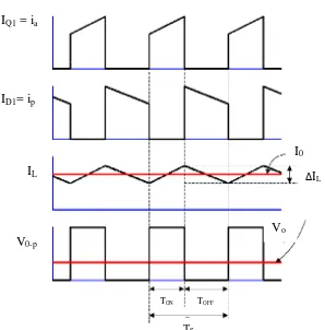
It occurs for light loads or low operating frequencies where the inductor current eventually hits zero during the switch open state in discontinuous mode. To prevent backward current flow, the diode will open. The small capacitances of the diode and MOSFET, acting in parallel with each other as a net parasitic capacitance, interact with inductor to produce an oscillation. The output capacitor is in series with the net parasitics capacitance but the capacitor is so large. When the capacitor is so large, it can be ignored in the oscillation phenomenon. Figure 2.6 shows the circuit of discontinuous mode of buck power stage converter and Figure 2.7 shows the discontinuous mode buck power stage waveforms in terms of voltage and current [3].
IQ1 = ia
ID1= ip
IL
V0-p
I0
∆IL
Vo
TON TOFF
11
Figure 2.6: Circuit of discontinuous mode of buck power stage converter [3]
Figure 2.7: The discontinuous mode buck power stage waveforms in terms of voltage and current [3]
IQ1
ID1
IL
V0-p
∆IL IPK
IPK
D*TS D2*T D3*T
12
2.1.1.3 Design of Buck Converter
A few considerations must be noted in order to design buck converter. Most buck converters are designed for continuous-current operation. When the switching frequency increases, the minimum size of the inductor to produce continuous current and the minimum size of capacitor to limit output ripple both decrease. At the same time, high switching frequencies are desirable to reduce the size of both the inductor and the capacitor. The tradeoff for high switching frequencies is increased power loss in the switches. Increased power loss in the
switches means that heat is produced. This heat produced will decrease the converter’s efficiency
and may require a large heat sink, offsetting the reduction in size of the inductor and capacitor. Typical switching frequencies need to avoid audio noise. For high-current and low-voltage applications, the synchronous rectification is preferred over using a diode for the second switch.
The voltage across the conducting MOSFET will be much less than that across a diode and resulting in lowers losses. To ensure continuous current operation, the inductor value should be larger than minimum inductor. The inductor wire must be rated at the rms current and the core should not saturate for peak inductor current. To the design specification to withstand peak output voltage and to carry the required rms current, the capacitor must be selected to limit the output ripple. The diode and switch must withstand maximum voltage stress when off and maximum current when on. The temperature ratings must not be exceeding often requiring a heat sink. Assuming ideal switches and an ideal inductor in the initial design is usually reasonable. In addition, the equivalent series resistance (ESR) of the capacitor should be included because it typically gives a more significant output voltage ripple than the ideal device and greatly influences the choice of capacitor size [4].
Important part in design this converter is by specify the input and output voltage of converter. Then find the duty ratio, D by using Equation 2.1 [5]
13
The next step is finding the average inductor current which is same with average current in the load resistor as Equation 2.2 [5]
IL = IR =
R Vo
(2.2)
Since the value of inductor current is known at Equation 2.2, the minimum and maximum values of inductor current are calculated as
IMAX = IL +
2 L i = R Vo + 2 1 [ L Vo
(1-D) T)] (2.3)
IMIN = IL
-2 L i = R Vo - 2 1 [ L Vo
(1-D) T)] (2.4)
The next step in design buck converter is by calculating the minimum inductance that required for continuous current.
LMIN =
f R D 2 ) 1 ( (2.5)
The value of inductance must greater than LMIN because to make sure that continuous
14
2.1.2 Voltage-Mode Control
Voltage-mode control is also known as the voltage feedback arrangement when applied to DC-DC converter. Voltage mode control is an easy way to design and implement and has good element to disturbance at the references input and it only contain single feedback loop from output voltage. Figure 2.8 shows the buck converter power and control stage [6].
Figure 2.8: The Buck Converter Power and Control Stage [6]
Non-ideal power train components are shown with parasitics such as capacitor equivalent
series resistance, RESR denoted explicitly and inductor DC resistance, RDCR. Second order
parasitics such as interconnection impedances and capacitor equivalent series inductance (ESL)
are not represented. The high side switch is driven by a PWM signal for time ton in each
switching period of duration TS. The duty cycle ration, D is given by Equation 2.7 [6]
Converter Power Stage
Type III Compensator
Modulator
Vref
Vramp
z1
p1 CC3
CC2
z1
15
D =
in out
S on
V V
T t
(2.7)
The low side switch is driven complementarily with duty cycle D’= 1-D. Both switches
of voltage-mode operate at fixed switching frequency fs= 1/TS. The output filter consists of
capacitor, Co and inductor, Lo. A conventional operational amplifier type voltage error amplifier
represents the epicenter of the control loop structure. The divided down output voltage at the error amplifier inverting input is usually termed the feedback node is compared to a fixed reference voltage and a compensated error signal is generated at the compensation node .This error signal is compared to a saw-tooth ramp voltage at the pulse width modulator comparator like an increase in compensation node leads to a commensurate increase in duty cycle command for the power stage. [7].
2.1.3 Current-Mode Control
There are three things to consider which current-mode operation, modulator gain is and slope compensation in current-mode control. Current-mode operation is an ideal current mode converter is only depending on the average or dc inductor current. The inner current loop turns the inductor into a voltage-controlled current source and effectively removing the inductor from the outer voltage control loop at dc and low frequency.
Modulator gain is dependent on the effective slope of the ramp presented to the modulating comparator input. Each modulating gain operating mode will have a unique characteristic equation for the modulator gain. Slope compensation is about the requirement for slope compensation which is dependent on the relationship of the average current to the value of current at the time when every sample is taken. In fixed-frequency operation, if the sampled current were equal to the average current, there would be no requirement for slope compensation.
![Figure 2.2: Buck Power Stage Schematic [2]](https://thumb-ap.123doks.com/thumbv2/123dok/513653.58452/16.612.111.559.379.554/figure-buck-power-stage-schematic.webp)
![Figure 2.3: Basic circuit of Buck Converter [3]](https://thumb-ap.123doks.com/thumbv2/123dok/513653.58452/17.612.170.477.298.434/figure-basic-circuit-buck-converter.webp)
![Figure 2.6: Circuit of discontinuous mode of buck power stage converter [3]](https://thumb-ap.123doks.com/thumbv2/123dok/513653.58452/20.612.179.447.362.651/figure-circuit-discontinuous-mode-buck-power-stage-converter.webp)
![Figure 2.8: The Buck Converter Power and Control Stage [6]](https://thumb-ap.123doks.com/thumbv2/123dok/513653.58452/23.612.178.523.261.526/figure-buck-converter-power-control-stage.webp)
