DOI: 10.12928/TELKOMNIKA.v14i4.3871 1253
Optimal Modulation Algorithm for Hybrid Clamped
Three-Level Inverter
Yi Liu*1, Guojun Tan2, Xiaoqun He3
School of Information and Electrical Engineering, China University of Mining and Technology, No.1, University Road, 221008, Xuzhou, China
*Corresponding author, e-mail: [email protected], [email protected], [email protected]
Abstract
The principle of a three phase hybrid clamped three-level inverter was presented. Taking sixty-four switch states into consideration, the operational states of hybrid clamped three-level inverter and different current circuits in different switch states were detailed derived. Optimal modulation algorithm was proposed based on the neutral small vectors by different combination, which can realize the automatic balancing of the neutral-point voltage with few switching cycles and did not need to measure the voltage of the clamped capacitors. The proposed modulation algorithm was also capable of restraining the turn-off over-voltage of the power switching devices effectively. Simulation results were given to verify the feasibility and correctness. Experimental results obtained by DSP-based implementation of the controller on 1 MW prototype show good performance in terms of DC-bus voltages regulation (small neutral point potential function and low DC ripple coefficient) and good sinusoidal current.
Keywords: Optimization method, Hybrid clamped inverter, Pulse width modulation, DC-voltage balance
Copyright © 2016 Universitas Ahmad Dahlan. All rights reserved.
1. Introduction
Nowadays, in order to meet the demands of the high-voltage grades and high-power inverter, an important trend in power electronic has been the replacement of the traditional two-level inverter by multitwo-level inverter [1-3]. With the development of power electronic technology, in [4-7], multilevel technology has been widely studied in the high-voltage and high-power system, grid-connected wind power system, active power filters, and many other fields. Currently, there is a large variety of such multilevel topologies available[8-9]. However, the three phase diode clamped three-level inverter is the most widely used topology. As an effective multilevel implementation, besides the characters of fewer power switching devices, lower input current harmonics, better sinusoidal and high adjustable power factor, diode clamped three-level inverter also has the advantages of bi-directional energy transfer, lower switching frequency and higher system efficiency, which can satisfy the requirements of higher voltage grades, higher power and lower harmonic pollution trend of inverter [10]. The operation and the control of three phase diode clamped three-level inverter have been researched during the last decade and both control and modulation methods have been presented in [11-12].
were proposed usually via the measure of DC-bus capacitor voltages and clamped capacitors. The purpose of this paper is to analyze the operation of the HCTLI, based on an analytical analysis of current circuit and clamped capacitor states, and to determine if a suitable modulation algorithm can implemented. Concentrated on the three phased HCTLI, a new PWM control algorithm is proposed by different optimal combination of neutral small vectors without the use of three clamped capacitor voltages measured in this paper. It can reduce the fluctuations of DC bus neutral voltage and restrain the over-voltages of the power switching devices. These functionalities of the proposed PWM control algorithm are demonstrated by both simulations and experimental results from a DSP controlled, the 1 MW rated inverter prototype.
2. Control Principle of HCTLI
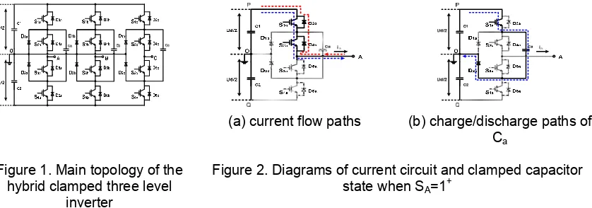
HCTLI using insulated gate bipolar transistor (IGBT) switches is presented in Figure 1. The main topology of the HCTLI consists of twelve power switches with anti-parallel diodes, each having voltage stress of Ud /2. There are six clamped diodes with three parallel clamped capacitors on phase legs and two DC-bus capacitors (C1,C2) in series on the DC side. The neutral point O of DC-bus is connected directly to three clamped midpoints.
To illustrate operation condition of HCTLI, phase A is set as an example to analyze. It is composed of clamped diodes (D1a~D2a), clamped capacitor Ca and four switches (S1a~S4a) with anti-paralleled diodes(D3a~D6a). Bidirectional current paths from load to the DC-bus potentials are achieved via switches (S1a~S4a) and diodes (D1a~D6a). Due to the clamped capacitor (Ca) of HCTLI, switches S2a and S3a can not work at the same time.
(a) current flow paths (b) charge/discharge paths of Ca
Figure 1. Main topology of the hybrid clamped three level
inverter
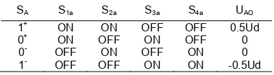
Figure 2. Diagrams of current circuit and clamped capacitor state when SA=1
+
The power switches states of phase A could be represented by SA. SA=1 +
indicates the on state of power switches S1a,S2a with S3a, S4a off. SA=0+ indicates the on state of power switches S1a, S3a with S2a, S4a off. SA=0− indicates the on state of power switches S2a, S4a with S1a, S3a off. SA=1− indicates the on state of power switches S3a, S4a with S1a, S2a off. Thus, the output voltage could be controlled by the switch states described above.
1) SA=1+ state
In SA=1
+
2) SA=0+ state
In Figure 3(a), if the phase current ia is positive in steady-state condition, the current flow along with the path: P→S1a→Ca→D5a→A. On the contrary, the current path will become A→S3a→D2a→C1→P. Whatever the direction of ia, the pole A is connected to below point of Ca. Three-level inverter has a problem that excessive high voltages may be applied to the power switches, when the floating mid-potential varies from the neutral point potential. In this state, the neutral point potential is changed constantly along with clamped capacitor charged and discharged. If the voltage UCa>UPO, the positive point P is connected to up point of the Ca at this moment. And the Ca would be discharged along with the path: A→S3a→Ca→D3a, while the phase current ia is negative. On the other hand if the voltage UCa<UPO, the Ca would be charged along with the path: P→S1a→Ca→D2a→O, until the two voltages meet the equation: UCa=UPO. The path of clamped capacitor charged and discharged is illustrated in Figure 3(b). The output voltage UAO is zero in SA=0+.
(a) current flow paths (b) charge/discharge paths of Ca
(a) current flow paths (b) charge/discharge paths of Ca Figure 3. Diagrams of current circuit and
clamped capacitor state when SA=0+
Figure 4. Diagrams of current circuit and clamped capacitor state when SA=0
3) SA=0
state
In contrast to the state of SA=0+, the power switches S1a, S3a are turned off with S2a, S4a on. When the phase current ia is positive in steady-state condition, the current flow along with the path: Q→C2→O→D1a→S2a→A. On the contrary, the current path will become A→D4a→Ca→S4a. The conduction path of current is illustrated in Figure 4(a). Similarly, the voltage across the clamped capacitor UCa is analyzed. As shown in Figure 4(b), if the voltage UCa>UOQ, the Ca would be discharged along with the path: D6a→Ca→S2a→A. On the other hand, if the voltage UCa<UOQ, the Ca will be charged along with the path: O→D1a→Ca→S4a→Q, until the voltage of the UCa has the same value as the voltage UOQ. The output voltage UAO between the inverter pole A and the neutral point O of DC-bus is also zero in SA=0−.
4) SA=1
state
The conduction path of current is presented in Figure 5(a), and the switches S1a, S2a are turned off and S3a, S4a turned on. Under steady-state condition, if the phase current ia is positive, the current flow along with the path: Q→D6a→D5a→A. Instead, the current flow path will become A→S3a→S4a→Q, when ia is negative. Whatever the direction of ia, the pole A is connected to negative point Q of the DC-bus, having the following equations: UAO=UQO=-0.5Ud. In the same way, if the voltage UCa>UOQ, the UCa remains constant. And the Ca would be discharged in the next switch state. Otherwise, the voltage UCa<UOQ, as shown in Figure 5(b), the Ca would be charged along with the path: O→D1a→Ca→S4a→Q, until the two voltages meet the equation: UCa=UOQ. The neutral point potential of the DC-bus is dropped sequentially in SA=1−.
Figure 5. Diagrams of current circuit and clamped capacitor state when SA=1 -Table 1. Switch states for phase A of HCTLI
SA S1a S2a S3a S4a UAO
1+ ON ON OFF OFF 0.5Ud
0+ ON OFF ON OFF 0
0- OFF ON OFF ON 0
1- OFF OFF ON ON -0.5Ud
To sum up, the switch states of phase A could be derived, and presented in Table 1. Similarly, this operating principle also applies to phase B and C. Because of four kinds of switch states for each phase, the HCTLI contains 43=64 kinds of switch state combinations. It makes control complicated, but the control accuracy will be improved with switch states increased.
3. DC-Bus Voltage Balance Analysis
HCTLI topology has been applied in medium and high voltage power applications due to the inherent advantages[20]. However, it also has the problem that the neutral point potential floated. It may lead to the issue that the power switches bear excessive high voltage. The HCTLI topology shows that stable neutral point potential determines whether the voltages of two DC-bus capacitors are balanced or not. In practical operation, the neutral point potential would fluctuate, leading to these two voltages of the DC-bus capacitors do not equal completely. Such voltage fluctuations may also result in distortion of the inverter output voltages, harmonic content increased and decrease in the output efficiency. Meanwhile, excessive high voltage that power switch devices withstood would cause the device itself breakdown and make the systematic reliability reduced greatly [16, 21]. And not only that, the life span of capacitance will also be greatly reduced because of severe capacitor voltages fluctuation, which would greatly damage AC drives. So it is important and significant to balance the DC-bus capacitor voltages.
It is generally known that HCTLI contains 64 kinds of switch states corresponding to 64 voltage space vectors, but among them are some redundant vectors. The neutral point potential is primarily influenced by these redundant vectors generated at the output of the inverter. The distribution of voltage space vectors is presented in Figure 6. It has 64 kinds of voltage space vectors, but there are only 19 kinds of valid and equivalent voltage space vectors after equivalent transformation, including one zero vector V0, six small vectors V1∼V6, six mid-vectors V7∼V12 and six large vectors V13∼V18. Among of them, the vector V0 contains 10 kinds of switch states and six switch states for each small vector, while each mid-vector corresponds to two switch states and each large vector corresponds to only one.
Different outputs of the inverter are generated by voltage space vectors based on the combination of 64 switch states in different ways. The analysis of these different output states of HCTLI shows that there are only seven output states associated with the DC-bus capacitors and the load. As Figure 7 shows, the direction of the arrows indicates the direction of loop-current.
0
V
13
V
7
V
14
V
8
V
15
V
9
V
16
V
10
V
17
V
11
V V18 12
V
6
V
5
V
4
V
3
V V2 1
V
(a) (b) (c) (d)
Figure 6. Diagram of voltage space vector distribution
(e) (f) (g)
The switch states that correspond to output states mentioned above are shown respectively:
(1) Output state "a": 1+0+0+, 0+1+0+, 0+0+1+; (2) Output state "b": 1+1+0+, 1+0+1+, 0+1+1+; (3) Output state "c": 0−1−1−, 1−0−1−, 1−1−0−; (4) Output state "d": 1−0−0−, 0−1−0−, 0−0−1−; (5) Output state "e": There are thirty six combinations for switch states, of which small vectors 1+0+0− and 1−0+0− all have six kinds of combinations. However, small vectors 1+0−0−, 1+1+0−, 0+1−1− and 1−0+0+ all have three kinds. Meanwhile, each of mid-vectors 1+0+1− and 1+0−1− also has six kinds of combinations;
(6) Output state "f": 1+1+1−, 1−1+1+, 1+1−1+; (7) Output state "g": 1+1−1−, 1−1+1−, 1−1−1+. Known from the analysis of the above: (i) In "a" and "b" output states, the neutral point potential rises, and the HCTLI outputs positive small vectors. The load is only connected to the capacitor C1, which forms a discharge circuit. At this moment, the voltage of C1 drops and the other rises. (ii) In "c" and "d", the neutral point potential drops, and the HCTLI outputs negative small vectors. The load is only connected to C2, and it forms a discharge circuit. In these two states, the voltage of C2 drops and the other rises. (iii) In "e", the HCTLI outputs neutral small vectors and mid-vectors. The two capacitors C1 and C2 are both connected to the load, which constituting two charge-discharge circuits. In theory, the small scale fluctuation of neutral potential can be achieved by some combinations of neutral small vectors and mid-vectors. (iv) In "f" and "g", the neutral point O has no connection and no current to the load. In this case, large vectors are generated. At the same time, the load connects the C1 and C2 directly, which have the same value in charge-discharge time and the average current of charge-discharge. In theory, as long as these two capacitors have the same parameters, the neutral point potential would keep constant. Accordingly, the neutral point potential is not affected by the large vectors.
In summary, selecting different vectors to synthesize the reference voltage space vectors will cause different effects on the neutral point potential.
4. Optimized Modulation Algorithm
Select the appropriate voltage space vectors is the core issue of SVPWM for HCTLI. The hexagonal plane of three-level voltage space vector is divided into six small hexagons of the same shape in conventional modulation algorithm, and then solved by two-level SVPWM in two-level voltage space vector plane [22]. However, this conventional modulation algorithm needs to further divide the reference voltage vector regions, because of its intersection area for some vectors. Figure 8(a) shows a new irregular division method adopted in this paper.
(a) Vector plane division (S =1, 2, 3, 4, 5, 6)
V V
(b) Composition for the reference voltage vector in small hexagonal section S=1, small
triangle section N=1
Figure 8. Diagrams of vector plane division and vector composition
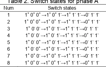
Table 2. Switch states for phase A
Num Switch states
1 1+ 0+ 0+ →1+ 0+ 1-→1+ 1- 1-→0- 1- 1 -2 1+ 0+ 0+ →1+ 0+ 1-→1+ 1- 1-→0+ 1- 1 -3 1+ 0- 0- →1+ 0- 1-→1+ 1- 1-→0- 1- 1 -4 1+ 0- 0- →1+ 0- 1-→1+ 1- 1-→0+ 1- 1 -5 1+ 0- 0+ →1+ 0- 1-→1+ 1- 1-→0- 1- 1
-6 1+ 0- 0+ →1+ 0- 1-→1+ 1- 1-→0+ 1- 1
-7 1+ 0+ 0- →1+ 0+ 1-→1+ 1- 1-→0- 1- 1
-The vector planes (S = 1, 2, 3, 4, 5, 6) are divided to ensure the reference vector can be assigned to a unique two-level voltage space vector plane. Take the vector plane divided (small hexagonal section S=1, small triangle section N=1) as an example to illustrate and calculate the switch operation time of voltage vectors selected. This triangle demarcates the valid and realizable location for the reference voltage vector. For HCTLI, SVPWM is implemented by synthesizing the reference vector using the three nearest vectors forming a triangle around it. As shown in Figure 8(b), when the reference voltage vector Vref lies to the first region N=1, the Vref can be jointly synthesized by three voltage vectors V1, V7 and V13. According to the principle of Volt-second balance, the operation times of V1, V7 and V13 would be derived at a sampling period through the voltage vectors correction and two-level SVPWM algorithm.
In Figure 8(b), the vector V'ref is corrected by Vref and V1 as the following function.
V
ref
V
ref
V
1 (1)Then, the Volt-second balance for the correct reference voltage can be expressed as:
2 13 1 7 0 1
2
/
V
T
V
T
V
T
T
V
ref
s
(2)HCTLI has 19 kinds of valid and equivalent states of the following type:
S
ABC
S
AS
BS
C
T (3)Switch states SX (x=A,B,C) take values in{1 +
, 0+ or 0−, 1−} presenting the per unit voltage of the phase with respect to the neutral point. Phase to neutral point voltages are given by:
U
AOU
BOU
CO
T
0
.
5
U
d
S
AS
BS
C
T (4)Thus, these voltages could be converted into the α-β coordinate using the following transformation:
CO BO AO ref refU
U
U
V
V
2
3
2
3
0
2
1
2
1
1
(5)The corresponding operation times (T0, T1 and T2) of V1, V7 and V13 are derived by equations (1)~ (5) respectively as follows:
d s ref s d s ref d s ref sU
T
V
T
U
T
V
T
U
T
V
T
T
T
T
T
2
3
3
2
3
5
.
4
3
3
2 1 2 1 0 (6)
Where: TS is the sampling period, Vrefα and Vrefβ are the components of Vref in α,β axis.
Take the reference voltage Vref shown in Figure 8(b) for example to analyze. As mentioned above, the reference voltage vector Vref can be jointly synthesized by three voltage vectors V1, V7 and V13 using the method of seven segment configuration. For SVPWM, the sequence of these three voltage vectors applied during a switching cycle is as follows:
V1→V7→V13→V1→V13→V7→V1
In the corresponding six switch states of small vector V1, both the positive small vector state {1+0+0+} and negative small vector state {0−1−1−} have a significant impact on the neutral point potential, and others are neutral small vector states{1+0+0−, 1+0−0+, 1+0−0−, 0+1−1−}. Mid-vectors have two kinds of states{1+0−1−, 1+0+1−}, while large vector has only one switch state. Therefore, eight kinds of vector states sequences to synthesize reference voltage vector could be obtained as shown in Table 2.
In order to ensure that each switch state change makes only one power switch turn on or off, appropriate switch state should be selected from the neutral small vector and mid-vector to meet the need. For the first of the switch state sequences, the same changes of three-phase switch states are between S1x and S4x (x = a, b, c). And the fourth of the switch states, the changes of three-phase power switch states are between S2x and S3x (x=a, b, c). Considering the power switch devices S2a and S3a can not turn on simultaneously because of the HCTLI topology, the AC load current flows through the primary channel of 1+ and 1−. In order to improve the quality of AC current waveform and reduce switch losses of power switch devices S2x and S3x (x = a, b, c), in the meantime, taking the fluctuations of the clamped capacitor into account, this paper chooses the first sequence to synthesize the reference voltage vector. The first sequence of switch states with corresponding operation times is shown as follow:
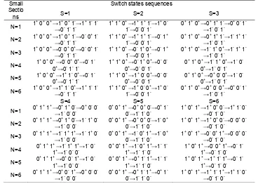
Similarly, the other vector sequences would be got to synthesize the voltage space vectors in other different sections of the vector plane following the principle proposed. The sequences of corresponding switch states for SVPWM algorithm are shown in Table 3.
Table 3. Switch states sequences for SVPWM
Small Sectio ns
Switch states sequences
S=1 S=2 S=3 N=1 1
+ 0+ 0+ →1+ 0+ 1-→1+ 1- 1
-→0- 1- 1
-1+ 1+ 0+ →1+ 1+ 1-→1+ 0
-1-→0- 0- 1
-0+ 1+ 0+ →0+ 1+ 1-→0+ 0- 1
-→1- 0- 1 -N=2 1
+
0+ 0+ →1+ 0+ 1-→0- 0+ 1
-→0- 1- 1
-1+ 1+ 0+ →1+ 1+ 1-→0- 1+ 1-→0- 0- 1
-0+ 1+ 0+ →0+ 1+ 1-→1- 1+ 1
-→1- 0- 1 -N=3 1
+
0+ 0+ →0- 0+ 0+→0- 0+ 1
-→0- 1- 1- 1 +
1+ 0+ →0- 1+ 0+→0- 1+ 1-→0- 0- 1- 0
+
1+ 0+ →1- 1+ 0+→1- 1+ 1
-→1- 0- 1
-N=4 1
+
0+ 0+ →0- 0+ 0+→0- 1 -0+→0- 1- 1
-1+ 1+ 0+ →0- 1+ 0+→0- 0 -0+→0- 0- 1
-0+ 1+ 0+ →1- 1+ 0+→1- 0 -0+→1- 0- 1 -N=5 1
+
0+ 0+ →1+ 1- 0+→0- 1 -0+→0- 1- 1
-1+ 1+ 0+ →1+ 0- 0+→0- 0 -0+→0- 0- 1
-0+ 1+ 0+ →0+ 0- 0+→1- 0 -0+→1- 0- 1 -N=6 1
+ 0+ 0+ →1+ 1- 0+→1+ 1- 1
-→0- 1- 1
-1+ 1+ 0+ →1+ 0- 0+→1+ 0
-1-→0- 0- 1
-0+ 1+ 0+ →0+ 0- 0+→0+ 0- 1
-→1- 0- 1
S=4 S=5 S=6
N=1 0
+
1+ 1+ →0+ 1+ 0-→0+ 0- 0
-→1- 0- 0
-0+ 0+ 1+ →0+ 0+ 0-→0+ 1 -0-→1- 1- 0
-1+ 0+ 1+ →1+ 0+ 0-→1+ 1- 0
-→0- 1- 0 -N=2 0
+
1+ 1+ →0+ 1+ 0-→1- 1+ 0
-→1- 0- 0- 0 +
0+ 1+ →0+ 0+ 0-→1- 0+ 0-→1- 1- 0- 1
+
0+ 1+ →1+ 0+ 0-→0- 0+ 0
-→0- 1- 0
-N=3 0
+
1+ 1+ →1- 1+ 1+→1- 1+ 0
-→1- 0- 0
-0+ 0+ 1+ →1- 0+ 1+→1- 0+ 0-→1- 1- 0
-1+ 0+ 1+ →0- 0+ 1+→0- 0+ 0
-→0- 1- 0 -N=4 0
+
1+ 1+ →1- 1+ 1+→1- 0 -1+→1- 0- 0
-0+ 0+ 1+ →1- 0+ 1+→1- 1 -1+→1- 1- 0
-1+ 0+ 1+ →0- 0+ 1+→0- 1 -1+→0- 1- 0 -N=5 0
+ 1+ 1+ →0+ 0- 1+→1- 0
-1+→1- 0- 0
-0+ 0+ 1+ →0+ 1- 1+→1- 1
-1+→1- 1- 0
-1+ 0+ 1+ →1+ 1- 1+→0- 1
-1+→0- 1- 0 -N=6 0
+
1+ 1+ →0+ 0- 1+→0+ 0- 0
-→1- 0- 0
-0+ 0+ 1+ →0+ 1- 1+→0+ 1 -0-→1- 1- 0
-1+ 0+ 1+ →1+ 1- 1+→1+ 1- 0
-In the same way, operation times of corresponding vectors in above regions could be obtained by the method proposed. Then, the pulses to control the switch devices on-off could be acquired based on SVPWM principle. The optimized modulation not only can meet the need to synthesize the voltage space vectors as a precondition, but also can balance the neutral point potential automatically. In addition to, it has good features of reducing the switch losses, decreasing switch frequency of S2x and S3x.
5. Simulation and Experiment
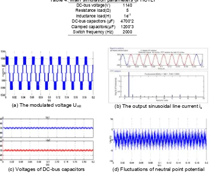
A detailed simulation for HCTLI has been built to verify the feasibility of the proposed algorithm based on Matlab/Simulink. The main parameters of simulation are listed in Table 4.
Figure 9 shows the simulation waveforms of HCTLI under steady-state operation. The modulated pole to pole voltage UAB and the output current ia are shown in Figure 9(a) and Figure 9(b) separately, and the total harmonic distortion of the measured current is 3.98%. DC-bus capacitors (C1, C2) voltages and the neutral point potential fluctuations are shown in Figure 9(c) and Figure 9(d). It is observed that the voltages of two DC-bus capacitors are almost balance. The fluctuation of the neutral point potential is very small, nearly ±5V.
Table 4. Main simulation parameters of HCTLI
DC-bus voltage(V) 1140 Resistance load(Ω) 5 Inductance load(H) 1e-3 DC-bus capacitors (μF) 4700*2 Clamped capacitors(μF) 1200*3
Switch frequency (Hz) 2000
(a) The modulated voltage UAB (b) The output sinusoidal line current ia
(c) Voltages of DC-bus capacitors (d) Fluctuations of neutral point potential
Figure 9. Simulation of voltage and current, DC-bus voltages and neutral point voltage
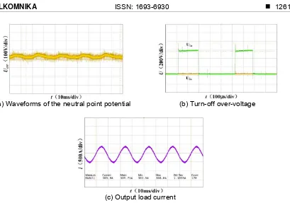
(a) Waveforms of the neutral point potential (b) Turn-off over-voltage
(c) Output load current
Figure 10. Diagrams of neutral point voltage, over-voltage in cutting off and current curves
Similar to the simulation results, the DC-bus voltage is stable and the ratio of the neutral point potential fluctuation is very small. As shown in Figure 10(a), the neutral point potential fluctuation is ±42V, and the DC ripple coefficient is 3.75% measured in the experiment. The waveform display good load current sinusoidal, while controlling the power switch devices turn-off over-voltage effectively. The turn-turn-off over-voltage of the power switch device S1a is about 200V, when the load current is 305A. Experiment fully illustrated this optimized modulation strategy is able to meet the needs of DC-bus voltage balance, effectively reducing the neutral point potential volatility and turn-off over-voltage of power switch.
6. Conclusion
The hybrid clamped three-level inverter and the operating conditions corresponding to power switch states were presented in this paper. The basic of the DC-bus capacitor voltages balancing was analyzed. A new SVPWM control algorithm was proposed to ensure balancing the DC-bus capacitor voltages and outputting sinusoidal current are met based on different optimal combination of neutral small vectors without the use of three clamped capacitor voltages measured in this paper. The operated sequences of switch states for this optimal modulation algorithm has been detailed presented. The functionality of the optimal SVPWM algorithm was proven with simulations an experiments of a 1 MW laboratory prototype. The match between the simulation and experimental results validates the the optimal SVPWM algorithm. The hybrid clamped three-level inverter is able to maintain balanced DC-bus capacitor voltages and make lower turn-off over-voltage. Furthermore, it provides better sinusoidal output load current.
References
[1] Lai JS, Peng FZ. Multilevel converters - a new breed of power converters. IEEE Transactions on Industry Applications. 1996; 32(3): 509-517.
[2] Suroso NFN, Noguchi T. Five-Level Common-Emitter Inverter Using Reverse-Blocking IGBTs. TELKOMNIKA Telecommunication Computing Electronics and Control . 2012; 10(1): 25-32. [3] Rodriguez J, Lai JS, Peng FZ. Multilevel inverters, a survey of topologies, controls, and applications.
IEEE Trans. Industry Applications. 2001; 49(4): 724-738.
[5] Holtz J, Qi X. Optimal control of medium-voltage drivesł-an overview. IEEE Transactions on Industry Electronics. 2013; 60(12): 5472-5481.
[6] Akagi H, Hatada T. Voltage balancing control for a three-level diode-clamped converter in a medium-voltage transformer-less hybrid active filter. IEEE Transactions on Power Electronics. 2009; 24(5): 571-579.
[7] Ng CH, Parker MA, Ran L, Tavner PJ, Bumby JR. A multilevel modular converter for a large light weight wind turbine generator. IEEE Transactions on Power Electronics. 2008; 23(3): 1062-1074. [8] Haitham AR, Holtz J, Rodriguez J, Ge B. Medium-voltage multilevel converters-state of the art,
challenges, and requirements in industrial applications. IEEE Transactions on Industry Electronics. 2010; 57(8): 2581-2596.
[9] Mathew J, Rajeevan PP, Mathew K, Azeez NA, Gopakumar K. Multilevel dodecagonal voltage space vector generation using flying capacitor topology for induction motor drives. in Proc. IEEE Energy Conversion Congress and Exposition (ECCE). 2012: 1136-1142.
[10] Nabea A, Takahashi I, Akagi H. A new neutral point clamped PWM inverter. IEEE Transactions on Industry Applications. 1981; 17(5): 518-523.
[11] Bharatiraja C, Raghu S. Comparative Analysis of Different PWM Techniques to Reduce the Common Mode Voltage in Three-Level Neutral-Point-Clamped Inverters for Variable Speed Induction Drives. International Journal of Electrical & Computer Engineering. 2013; 3(1): 105-116.
[12] Zhang YC, Zhao ZM, Zhu JG. A hybrid PWM applied to high-power three-level inverter fed induction-motor drives. IEEE Transactions on Industrial Electronics. 2011; 58(8): 3409-3420.
[13] Khajehoddin SA, Bakhshai A, Jain PK. A simple voltage balancing scheme for M-level diode-clamped multilevel converters on a generalized current flow model. IEEE Transactions on Power Electronic. 2008; 23(5): 2248-2259.
[14] Verne SA, Gonzalez SA, Valla MI. An optimization algorithm for capacitor voltage balance of N-level diode clamped inverters. In Proc. IEEE Conference on Industrial Electronics. Orlando, Florida, USA. 2008: 3201-3206.
[15] Vaseee S, Sankerram BV. Voltage Balancing Control Strategy in Converter System for Three-Level Inverters. International Journal of Electrical & Computer Engineering. 2013; 3(1): 7-14.
[16] Gupta AK, Khambadkone AM. A simple space vector PWM scheme to operate a three-level NPC inverter at high modulation index including over modulation region with neutral point balancing. IEEE Transactions on Industry Applications. 2007; 43(3): 751-760.
[17] Chaves M, Margato E, Silva JF, Pinto SF. New approach in back-to-back M-level diode-clamped multilevel converter modelling and direct current bus voltages balancing. IET Power Electronics, 2010, 3(4): 578-589.
[18] Ning DL, Tong XQ, Shen M, Xia W. The experiments of voltage balancing methods in IGBTs series connection. In Proc. IEEE Conference on Asia-Pacific Power and Energy Engineering. Chengdu, China. 2010: 1-4.
[19] Kim YS, Seo BS, Hyun DS. A novel structure of multilevel high voltage source inverter. In Proc. IEEE Conference on Computer, Communication, Control and Power Engineering. Beijing, China. 1993: 503-508.
[20] Zhao J, He X, Zhao R. A novel PWM control method for hybrid-clamped multilevel inverters. IEEE Trans. Industrial Electronics, 2010; 57(7): 2365-2373.
[21] Celanovic N, Boroyevich D. A comprehensive study of neutral-point voltage balancing problem in three-level neutral-point-clamped voltage source PWM inverters. IEEE Transactions on Power Electronics. 2000; 15(2): 242-249.