International Journal of the Physical Sciences Vol. 6(5), pp. 1096-1111, 4 March, 2011 Available online at http://www.academicjournals.org/IJPS
DOI: 10.5897/IJPS10.281
ISSN 1992 - 1950 ©2011 Academic Journals
Full Length Research Paper
Three phase inverter control using DSP controller for
dynamic voltage restorer (DVR) application
Rosli Omar
1* and N. A Rahim
21
Faculty of Electrical, University Teknikal Malaysia Melaka,Karung Berkunci 1752, Pejabat Pos Durian Tunggal, 76109, Durian Tunggal, Melaka.
2
Centre of Research for Power Electronics, Drives, Automation and Control, University of Malaya, 50603 Kuala Lumpur, Malaysia.
Accepted 25 February, 2011
This paper discusses the control technique improvement of a three-phase inverter using direct-quadrature-zero (d-q-0) controller based on DSP TMS320F2812 for dynamic voltage restorer (DVR) applications. The output of the inverter is then connected to a voltage grid via a second order filter and injection transformer. The control algorithms are developed using TMS320F 2812 DSP. The proposed technique achieves voltage regulation with low total harmonics distortion (THD) for both voltage and current. This paper also highlights a series of discussion, analysis and studies performed on the proposed control technique, including L-C filter design issue and the concept of DVR in the distribution system. An analysis and experimental results validate the effectiveness of the DSP controller in mitigating voltage sags and harmonics issues in the distribution system
Key words: TMS320F2812 DSP, inverters, dynamic voltage restorer (DVR), total harmonic distortion (THD), filter.
INTRODUCTION
With the rapid technology advancements in industrial control processes, electric utilities are experiencing more demanding requirements on the power quality from the large industrial power consumers. Such power quality problems have been better appreciated when the price paid, due to the economic losses caused by them, is large. These concerns are reflected in the newer versions of power quality standards, such as IEEE 1159-1995 (IEEE, 1995) and IEC6100-4-30 (IEC, 2003).
Among the various power quality problems, the voltage sag, usually resulting from the faults on parallel transmission/distribution feeders, is attracting quite a large amount of attention from researchers of both industry and academia (Nelson et al., 2004; Woodley,
*Corresponding author. E-mail: [email protected].
2000). A definitive solution to this problem at large power levels has been commonly called dynamic voltage restorer (DVR), under the rubric of the custom power concept introduced by EPRI (Hingorani, 1999). The main function of DVR is to mitigate the voltage sag, although sometimes, additional functions such as harmonic compensation and reactive power compensation are also integrated to the device.
Power quality standards for connection of an inverter to the grid are still under development, since previously, there have been a few similar high power applications. In (IEEE, 1992) it is stated that the power quality is determined by the voltage quality, when the voltage is a controlled o variable.
voltage sags and interruptions for electrical networks is thoroughly described in the work of Bollen (1999). Dynamic voltage restorer (DVR) has been recognized as a cost effective solution for the protection of sensitive loads from voltage sags (Fitzer et al., 2004). DVR is primarily used for the distribution system by injecting compensating voltage in series with the supply network when an upstream fault is detected (Zhan et al., 2001; Kara et al., 1998; Nielsen et al., 2004). Loads connected downstream of the DVR are thus protected from any voltage sags caused by faults elsewhere on the network.
In order to deliver a good ac power, the controlled pulse width modulation (PWM) inverter and L-C output filter have to convert a dc voltage source (for example, batteries) to a sinusoidal ac voltage with low voltage THD and fast transient response under load disturbances. Another important aspect of power quality is harmonic distortion. General requirements for harmonic distortion can be found in standard as seen in the work of Casadei et al. (2005) and particularly for connection of distributed resources to grid in Iqbal et al. (2006).
PWM control is the most powerful technique that offers a simple method for control of analog systems with the processor’s digital output (Grandi et al., 2006). With the availability of low cost, high performance DSP chips, characterized by the execution of most instructions in one instruction cycle, complicated control algorithms can be executed with fast speed, making very high sampling rate possible for digitally-controlled inverters (Hadiouche et al., 2006).
Recently, techniques to produce an output voltage with low total harmonic distortion (THD) in a three-phase pulse width modulation (PWM) inverter have been proposed (Maria et al., 2007).
In this paper, the implementation of a digital signal processor (DSP) using an improved d-q-0 based controller was done in order to control inverter pulses, and then the output of the inverter was injected through the injection transformer of the DVR.
The improvement of the controller is easy to design and does not depend much on circuit parameters. The dc value of the capacitor and harmonic ripple current due to input power circuit can be reduced. The controller can detect any disturbance in the network very fast.
THE CONCEPT OF THE DVR IN THE DISTRIBUTION SYSTEM
DVR operation and components
A power electronic converter based series compensator that can protect critical loads from all supply side disturbances other than outages is called a dynamic
Omar and Rahim 1097
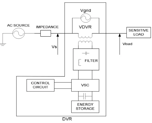
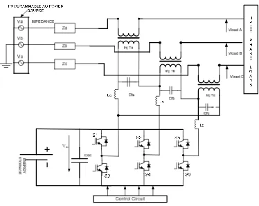
voltage restorer (Blaabjerg et al., 2004; Ojo et al., 2005). Figure 1 shows the configuration of the DVR consisting of an inverter, series or injection transformer, inverter control system and energy storage. The main function of a DVR is the protection of sensitive load from any disturbances coming from network. The main components of the DVR are summarized below;
Voltage injection transformers
In a three-phase system, either three single-phase transformer units or one three phase transformer unit can be used for voltage injection purpose (Zhan et al., 2000).
Capacitor
DVR has a large DC capacitor to ensure stiff DC voltage input to inverter.
Inverter
An Inverter system is used to convert dc storage into ac form (Ravi et al., 2007). Voltage source inverter (VSI) of low voltage and high current with step up injection transformer is used for this purpose in the DVR compensation technique (Perera et al., 2006).
Passive filters
Filters are used to convert the inverted PWM waveform into a sinusoidal waveform. This is achieved by eliminating the unwanted harmonic components generated VSI action. Higher orders harmonic components distort the compensated output voltage (Zhan et al., 2000).
Energy storage unit
It is responsible for energy storage in DC form. Flywheels, batteries, superconducting magnetic energy storage (SMES) and super capacitors can be used as energy storage devices. It supplies the real power requirements of the system when DVR is used for compensation (Banaei et al., 2006).
1098 Int. J. Phys. Sci.
Figure 1. Conventional circuit configuration (Nielsen and Blaabjerg, 2005).
by the loads. During normal operation, the capacitor receives energy from the main supply source. When voltage dip or sags are detected, the capacitor delivers dc supply to the inverter. The inverter ensures that only the missing voltage is injected to the transformer. A relatively small capacitor is present on dc side of the PWM solid state inverter, and the voltage over this capacitor is kept constant by exchanging energy with the energy storage reservoir. The required output voltage is obtained by using pulse-width modulation switching pattern. As the controller will have to supply active, as well as reactive power, some kind of energy storage is needed. In the DVRs that are commercially available now, large capacitors are used as a source of energy (Chris et al., 2004). Other potential sources being considered are; battery banks, superconducting coils, and flywheels (Zhan et al., 2001; Mostafa et al., 2007). The concept of compensation techniques being used in DVR can be divided into two methods as discussed further (Monsef et al., 2006; Kasuni, 2007).
In-phase compensation method
The injection voltage is in phase with the source voltage. When the source voltage drops due to sagging problems in the network, the injection voltage produced by the Voltage Source Inverter (VSI) will inject the missing voltage based on the drop voltage magnitude. This method can be shown in Figure 2.
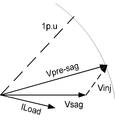
Pre-sag method
In this method, there is a difference between Vpre-sag and the sag voltage (Vsag). The injection voltage will inject the difference voltage between them as shown in Figure 3.
Inverter’s output filter design dimensioning of a DVR
A general use of a filter is to perform some frequency-selective isolation between sources which is viewed as having a range of frequency components and a load to which it will pass only some of those frequency components and reject others.
A LC filter often works best in the dc mode if the load has switches, because a large L would face the dc supply and the large capacitor of high quality would provide low impedance for the switching frequency as shown in Figure 4. The transfer function H( jω) may relate the output and input voltages or current of the filter. In this case, the relationship between the output voltage and the input voltage is as follow:
i o
V
V
jw
H
(
)
=
Figure 2. The diagram of in-phase compensation technique.
Figure 3. The diagram of pre-sag compensation
technique. L c L L i o Z L j LC j Z j V V jw H
ω
ω
ω ω − + = + = 2 1 1 1 1 1 ) ( (1)Omar and Rahim 1099
Figure 4. LC filter of a DVR system.
The values of L and C can be derived based on the following steps:
The first step is choose the suitable type of the filter that needs to be implemented in the circuit;
The second step is to calculate the designed impedance from the minimum value of the voltage (Vmin) divided by
the maximum current (Imax) which is
Z
LI
V
=
(min) (min) ;The third step is to determine the cutoff frequency fo; Finally, compute the component values
o
d
f
Z
L
π
2
=
(2)d o
Z
f
C
π
2
1
=
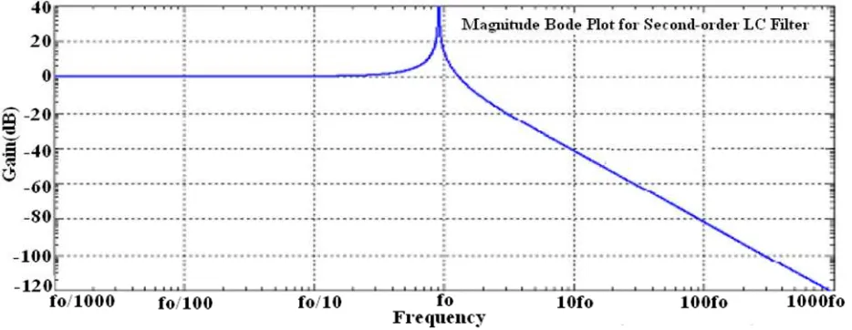
(3)The frequency response curve of Equation (1) is shown in Figure 5. From the figure, it is recognized that the filter has desirable characteristics near fundamental frequency region.
CONTROL DEVELOPMENT OF THE DVR
1100 Int. J. Phys. Sci.
Figure 5. The frequency response curve of the LC filter.
ranging from 0.9 pu to 0.5 pu of a 1-pu nominal (Zhan et al., 2001; Monsef et al., 2006; Zhou and Wang, 2002; Rodriguez et al., 2007).
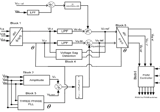
The proposed d-q-0 operated DVR system is implemented using DSP board. The general requirement of a control scheme is to obtain an ac waveform with minimum total harmonic distortion (THD) and best dynamic response against supply and load disturbance when the DVR is operated for voltage sag compensation (Mahinda et al., 2003). The main aspects of the control system are shown in Figures 6 and 7, and include the following blocks:
Block 1: used to convert the three phase load voltages (VLa, VLb, VLc ) into the α-β-o coordinates as in Equation (4) = Lc Lb La o V V V Q V V V β α (4)
Where Q =
− − − 2 1 2 1 2 1 2 3 2 3 0 2 1 2 1 1 3 2
Block 1 is also used to convert the three phase load voltages (VLa, VLb, VLc ) into the α-β-o coordinates as in Equation (1). The three phase load voltages reference components Vα-ref, Vα-ref and Vo ref can be converted to Vd
ref and Vq ref as shown in Equation (5).
− = β α θ θ θ θ V V V V q d cos sin sin cos 3
2 (5)
Transformation to dqo to abc
− = q d V V V V θ θ θ θ β α cos sin sin cos 3
2 (6)
− − = o c b a V V V V V V β α 1 2 3 5 . 0 1 2 3 5 . 0 1 0 1 (7)
Block 2: is considered as source voltages (Vsa, Vsb, Vsc). The amplitude of AC voltage at the sources (Vsource) can be calculated as follow;
( )
( )
( )
+
+
=
2 2 23
2
sc sb
sa
source
V
V
V
V
(8)
Omar and Rahim 1101
θ
θ
θ
Figure 6. Block diagram control of the proposed scheme of DVR implemented in DSP.
phase difference between the input and the output signals is measured using a phase detection scheme and passed through a loop filter to generate an error signal driving a voltage-controlled oscillator (VCO) which generates the output signal.
Block 4: is the detection scheme for the voltage unbalanced compensator. From Figure 6, it shows that, the synchronous frame variables, Vd and Vq are used as inputs for low pass filters to generate voltage references in the synchronous frame.
Block 5: receives the components of the load voltage vectors Vd ref and Vq ref and transforms them to three phase coordinates using Equations (5) and (6). The generation voltages are used as the voltage reference. The DC link error in Figure 6 is used to get optimized
controller output signal because the energy on the DC link will be changed during the voltage sag.
Block 6: is the PWM block which provides the firing for the Inverter switches (PWM1 to PWM6). The injection voltage is generated according to the difference between the reference load voltage and the supply voltage and is applied to the voltage source Inverter (VSI).
EXPERIMENTAL SET-UP
1102 Int. J. Phys. Sci.
Figure 7. DSP controlled three -phase PWM inverter using d-q-0 controller.
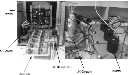
Figure 8. Experimental set-up of the power circuit consists of three phase inverter, DSP and filter scheme.
hardware designed is as shown in Table 1. The incoming three phase supply voltage is fed into the AC power source. The DVR injects active and reactive power into the system via three series injection transformers. The DVR obtains its active power from a
lead acid battery bank.
Omar and Rahim 1103
Figure 9. Configuration of the proposed DVR.
Table 1. Main specification of the DVR.
Nominal grid voltage 120 V (L-L)
Nominal load voltage 120 V(L-L)
Switching/sampling frequency 5 KHz
Max. inverter dc-bus voltage 120 V
Capacitor of dc- bus 26 uF
Filter inductance 3.947 mF
Filter capacitance 6.417 uF
to the analog digital converter of the DSP. The sampling times are governed by the DSP timer called a CpuTimer0 which generates periodic interrupt at each sampling times. The Interrupt Service Routine (ISR) will read the sampling value of the voltage and current source from the analog digital converter (ADC). The DSP controller offers a display function, which monitors the disturbances in the real time. The control algorithm which was proposed earlier is tested with a control using DSP TMS 320F 2812. The controller has its own ADC converters and PWM pulse outputs. The inputs of a 3-leg voltage source inverter (VSI) are the PWM pulses which are generated by the digital controller. The three phase supply voltage is measured continuously and is then compared with the reference voltage in order to regulate load voltage response. If any disturbances occur between the supply voltage and load voltage, the different voltage between them will be compensated. The
amount of compensated voltage needed to be injected is calculated and the results of the supply, load and compensated voltages will be processed by the DSP and injected to the IGBT switching scheme (PWM1 to PWM 6).
RESULTS AND DISCUSSION
1104 Int. J. Phys. Sci.
(a)
(b)
( c )
Omar and Rahim 1105
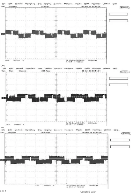
Figure 11. The line voltage of phase A ,B and C after connecting the filter.
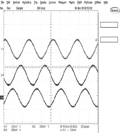
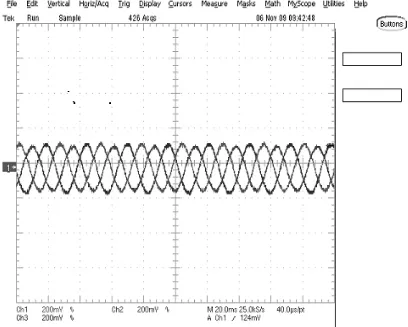
shown in Figure 11(a, b, c). The three phases of the voltages of the inverter’s output with LC filter were also measured. Figure 12 shows the results of the three phase waveform voltages with LC filter.
The phase voltage and phase current on the load side were also measured and it showed that the voltage and current are in phase and their waveforms are smoothed sinusoidal without any distortion. Figure 13 shows the results of phase voltage and current, which are in phase. Due to in phase voltage and current on the load side
without any distortion there is stable power factor and the value is almost one.
1106 Int. J. Phys. Sci.
Figure 12. Three phase voltages at output of the inverter.
Omar and Rahim 1107
H
a
rm
o
n
ic
c
o
m
p
o
n
e
n
t
(%
)
100
80
60
40
20
0
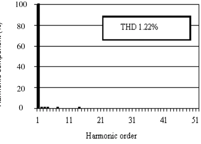
Figure 14. THD for the phase voltage.
H
a
rm
o
n
ic
co
m
p
o
n
e
n
t
(%
)
100
80
60
40
20
0
Figure 15. THD for the phase current.
Figure16 shows the currents of the output inverter with the balanced load connected. It can be seen from the figure the controller is able to stable the inverter current from distortion.
1108 Int. J. Phys. Sci.
Figure 16. Current at the inverter output.
Figure 17. Waveform of supply voltage, injection voltage and load voltage.
inject the missing voltages in the distribution system. The capabilities of the DVR to inject the appropriate voltage caused the load voltage maintained constant.
The waveforms of the three phase balanced voltage sags, three phase injection and load voltages are shown in Figure 18 (a, b, c). The three phase balanced sags
Omar and Rahim 1109
(a)
(b)
(c )
Figure 18. (a) Three phase balanced voltage sag; (b) injection voltages; (c) mitigation load
1110 Int. J. Phys. Sci.
(a)
(b)
Figure 19. (a)Total harmonic distortion current (THDI) under unstable dc-link; (b) total
harmonic distortion current (THDI) under stable dc-link.
the load voltage constant at the nominal value. The injection voltage by the DVR can be seen in Figure 18(b). The load recovery at its nominal value during the three phase sags is shown in Figure 18(c).
In the proposed system of the DVR configuration as shown in Figure 9, the DC link capacitor is used and it acts as an energy storage element of the DVR. In the calculation to determine the value of the DC link capacitor, the rating of IGBT must be considered. DC link
Conclusion
This paper presents the analysis and design of a digitally controlled three-phase PWM inverter based on DSP control application using d-q-0 controller in order to generate three-phase voltage for dynamic voltage restorer application. The basics of software optimization and hardware installation for proposed system have been presented in detail. The proposed technique achieves voltage regulation with low total harmonics distortion (THD) for both voltage and current at the connected load. The very close agreement of experimental results illustrates the efficiency, accuracy and dynamic response of DSP based PWM inverter design using d-q-0 controller. Three-phase voltages produced by inverter will be used to inject the missing voltage through injection transformer. The injection voltages through injection transformer are able to mitigate voltage sags and the load voltage is maintained at its nominal value. The experimental results also show that the capabilities of the proposed DVR along with the proposed controller DSP based in compensating voltage sags in low voltage distribution system.
ACKNOWLEDGEMENTS
The authors wish to thank University of Malaya (UM) and University Teknikal Malaysia (UTeM) for providing grants under grant PS002/2009C for this project.
REFERENCES
Banaei MR, Hosseini SH, Khanmohamadi S, Gharehpetian GB (2006). Verification of a new energy control strategy for dynamic voltage restorer by simulation. ELSEVIER Simul. Model. Pract. Theory, 14: 113-125.
Blaabjerg F, Chen Z, Kjaer S (2004). “Power electronics as efficient interface in dispersed power generation systems.” IEEE Trans. Power Electron., 19(5): 1184–1194.
Bollen M (1999). Understanding Power Quality Problems, Voltage Sags and Interruptions” Piscataway. New York: IEEE Press, 2000. Casadei D, Serra G, Tani A, Zarri L (2005). “Multi-phase inverter
modulation strategies based on duty-cycle space vector approach.” Proceedings of Ship Propulsion and Railway Systems Conference SPRTS, Bologna, Italy, pp. 222-229.
Chris F, Mike B, Peter G (2004). Voltage sag detection technique for a dynamic voltage restorer. IEEE Trans. Ind. Appl., 40(1).
Grandi G, Serra G, Tani A(2006). “Space vector modulation of a seven-phase voltage source inverter.” Proceedings of International Symposium Power Electronics. Elec. Drives Autom. Motion SPEEDAM Taormina, Italy, CDROM Pap., pp. 6-8.
Hadiouche D, Baghli L, Rezzoug A (2006). “Space vector PWM techniques for dual three-phase AC machine: Analysis, performance evaluation and DSP implementation.” IEEE Trans. Ind. Appl., 42(4): 1112-1122.
IEEE Std. (1159–1995). “Recommended Practice for Monitoring Electric Power Quality.”
Omar and Rahim 1111
IEEE Std. (1159–2000). “Recommended Practice for Monitoring Electric Power Quality.”
Iqbal A, Levi E, Jones M, Vukosavic SN (2006). “Generalised sinusoidal PWM with harmonic injection for multi-phase VSIs.” Proc. IEEE Power Elec. Spec. Conf. PESC, Jeju, Korea, pp. 2871-2877. Nielsen JG, Blaabjerg F (2005). A Detailed Comparison of System
Topologies for Dynamic Voltage Restorers. IEEE Trans. Ind. Appl., 41(5).
Kara A, Dahler P, Amhof D, Gruning H (1998). Power supply quality improvement with a dynamic voltage restorer (DVR), in Proc. IEEEAPEC., 2: 986-993.
Kasuni P, Daniel S, Arulampaiam A, Sanath A (2006). “Automated Control Technique for A Single Phase Dynamic Voltage Restorer.” IEEE., pp. 63-68.
Mahinda D, Vilathgamuwa AADR, Perera SS (2003),“Voltage sag compensation with energy optimized dynamic voltage restorer. IEEE Trans. Power Electron., 18(3): 928-936.
Maria IM, Enrique RC, Fermin BG (2007). “Comparison of Control Strategies for Shunt Active Power Filters in Three-Phase Four-Wire Systems.” IEEE Trans. Power Electron., 1: 229-236.
Monsef H, Tamimi B (2006). "The Operation Of DVR in Voltage Sag Mitigation Using EMTP." Int. J. Factory Autom. Robot. Soft Comput., 2: 102-106.
Mostafa IM, Ehab E-SF, Magdy SMA (2007). A new approach to control DVR based on symmetrical components estimation. IEEE Trans. Power Deliv., 22(4).
Nielsen G, Newman M, Nielsen H, Blaabjerg F (2000). Control and testing of a Dynamic Voltage Restorer (DVR) at medium voltage level. IEEE Trans. Power Electron., 19(3): 806–813.
Nielsen JG, Newman M, Nielsen H, Blaabjerg F (2004). “Control and testing of a dynamic voltage restorer (DVR) at medium voltage level.” IEEE Trans. Power Electron., 19(3): 806.
Ojo O, Dong G (2005). “Generalized discontinuous carrier-based PWM modulation scheme for multi-phase converter-machine systems.” Proc. IEEE Ind. Appl. Soc. Annu. Meeting IAS, Hong Kong, CD-ROM Pap., IAS38: 3.
Pedro R, Josep P, Joan B (2007). Decoupled double synchronous reference frame PLL for power converters control. IEEE Trans. Power Electron., 22(2).
Ravi KSV, Siva S, Nagaraju S (2007). “Simulation of D-Statcom and DVR in Power Systems.” ARPN J. Eng. Appl. Sci., 2(3).
Testing and Measurement Techniques (2003). Power Quality Measurement Methods. IEC 61000-4-30.
TMS320C281x Event Manager Reference Guide (SPRU065). Texas Instrument. TMS320C281x Analog to Digital Converter Reference Guide (SPRU066), Texas Instrument.
Woodley NH, Morgan L, Sundaram A (2000). “Experience with an inverter-based dynamic voltage restorer.” IEEE Trans. Power Deliv., 14(3): 1181.
Zhan C, Fitzer C, Ramachandaramurthy VK, Arul AA, Barnes M, Jenkins N (2001). Software phase-locked loop applied to dynamic voltage restorer (DVR). Proc. IEEE- PESWinter Meeting, pp. 1033-1038.
Zhan C, Barnes M, Ramachandarmurthy VK, Jenkins N (2000). “Dynamic Voltage Restorer with a battery Energy Storage for Voltage Dip Mitigation.” Eighth Int. Conf. Power Electron. Variable Speed Drives, 18-19: 360-365.