AENSI Journals
Australian Journal of Basic and Applied Sciences
ISSN:1991-8178Journal home page
Corresponding Author: Faiz Arith., Faculty of Electronics Engineering & Computer Engineering, Universiti Teknikal Malaysia Melaka, Hang Tuah Jaya, 76100 Durian Tunggal, Melaka, Malaysia.
E-mail: [email protected]
Prospects of molybdenum thin film for solar cell application from AFM analysis
1,3Faiz Arith, 1,2Nowshad Amin, 1Puvaneswaran Chelvanathan, 1,3M. Idzdihar Idris
1Department of Electrical, Electronic & System Engineering, Faculty of Engineering and Built Environment, Universiti Kebangsaan
Malaysia, Bangi 43600, Selangor, Malaysia.
2Solar Energy Research Institute, Universiti Kebangsaan Malaysia, Bangi 43600, Selangor, Malaysia.
3Faculty of Electronics Engineering & Computer Engineering, Universiti Teknikal Malaysia Melaka, Hang Tuah Jaya, 76100 Durian
Tunggal, Melaka, Malaysia.
A R T I C L E I N F O A B S T R A C T
Article history:
Received 1January 2014 Accepted X January 2014 Available online February 2014
Keywords:
CdTe, CIGS, Molybdenum, RF Sputtering.
Molybdenum (Mo) was grown on soda lime glass by the radio frequency (RF) magnetron sputtering deposition method to characterize the prospect feature to be used as solar cell back contact. 10 samples were sputtered with different suitable parameter by varying RF target power, argon gas pressure and growth temperature. Then all the samples were analyzed by atomic force microscopy (AFM) to determine their features and specification. The results include molybdenum thin film characteristics of roughness, grain size and root mean square (RMS) is obtained. From these characterization results the paramount parameter condition is obtained which at 200 °C, 6.6 mTorr and 75 Watt. These optimized results can be used in future work for fabricating of molybdenum as back contact layer for solar cell application. In conclusion, this study has obtained the optimized parameter in term of growth temperature, argon (Ar) gas pressure and radio frequency (RF) power for molybdenum growth on thin films that compatible and can be integrated not only for solar cell application but with wide variety of MEMS/NEMS devices.
© 2014 AENSI Publisher All rights reserved. To Cite This Article: Faiz Arith, Nowshad Amin, Puvaneswaran Chelvanathan, M. Idzdihar Idris., Prospects of molybdenum thin film for solar cell application from AFM analysis. Aust. J. Basic & Appl. Sci., 8(2): 87-92, 2014
INTRODUCTION
World population growth over the years causing the need of electricity is becoming vital. With the increasing cost of electricity from conventional sources and the effect of global warming it is essential to shift to renewable energies to meet the global energy demand. Photovoltaic (PV) solar cell technology is one of the most promising options of all the renewable technologies that can convert sunlight into electricity (Faiz et al., 2014; Green, 2000). Among the various PV technologies, such as Si based, a-Si:H and thin film; CIGS and CdTe solar cell which belonging to thin film solar cell group have the large potential for cost reduction with respect to power generation efficiency. The highest reported efficiencies of a CIGS and CdTe solar cell are 19.6% and 18.3%, respectively (Green et al., 2013).
MATERIALS AND METHODS
Fabrication of Molybdenum Thins Films:
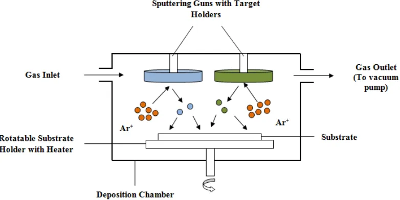
In this study, molybdenum is grown on a 10 soda lime glass (SLG) with different parameter by using radio frequency (RF) magnetron sputtering method. Hence, RF sputtering process is a very important thin film deposition method in this study. Sputtering deposition process is a physical vapor deposition (PVD) process whereby thin film layers are produced from the bombardment of energetic particles onto a target, knocking off the atoms of the target material. Film growth occurs on the substrate usually placed on the bottom of the deposition chamber as shown in the figure 1 below.
Fig. 1: Schematic diagram of sputtering deposition chamber layout
The energetic particle that is often used in sputtering process is ionized argon gas atoms which are supplied into the deposition chamber via the gas inlet. The sputtering gun has its own power supply with operating frequency of 13.56 MHz During deposition process, initially the argon gas atoms which are introduced are neutral and collide with each other creates argon gas ions which are positively charged (argon atoms loses an electron). The alternating polarity of the electric field induced by the RF frequency will attract and repel the argon ions repeatedly against the target material, causing the target material atoms to be knocked off. To promote a uniform film growth, substrate is rotated with the rotatable substrate holder and the rotation speed can be varied. Substrate can also be heated to enhance the nucleation process during the film growth. Sputtering process offers a flexible platform for thin film deposition research as there are numerous variables that can be manipulated and varied in order to observe the effects on the film growth condition (Davidse, 1967).
Parameter variables:
In this research, sputtering parameters for the buffer layer deposition process that are varied are operating pressure (correlates with argon gas flow rate, sccm), RF sputtering power, and substrate deposition temperature. Table 1 below shows the sputtering parameters that are investigated in this study.
Table 1: RF magnetron sputtering parameter
Sputtering Parameter Range
Operating Pressure 6.6– 20 [mTorr]
RF Power 50 – 125 [Watt]
Growth Temperature Room Temperature (RT) – 300 [°C]
AFM characterization produces the results of surface morphology in term of roughness, RMS and grain size. These results play as a main factor consider for the best condition to deposit molybdenum thin film and suitable for solar cell application
RESULTS AND DISCUSSION
Atomic Force Microscopy (AFM):
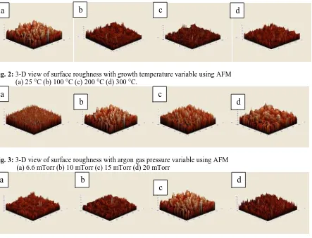
by cantilever then measured as scanned surface structure (Gross et al., 2009). In this research, the AFM test is performed to the molybdenum sputtered layer to determine the roughness and grain size. Figure 2 to figure 4 show the 3-D view of the molybdenum layer by using AFM with different parameter.
Fig. 2: 3-D view of surface roughness with growth temperature variable using AFM (a) 25 °C (b) 100 °C (c) 200 °C (d) 300 °C.
Fig. 3: 3-D view of surface roughness with argon gas pressure variable using AFM
(a)6.6 mTorr (b) 10 mTorr (c) 15 mTorr (d) 20 mTorr
Fig. 4: 3-D view of surface roughness with RF power variable using AFM
(a)50 Watt (b) 75 Watt (c) 100 Watt (d) 125 Watt
Roughness and Root Mean Square (RMS):
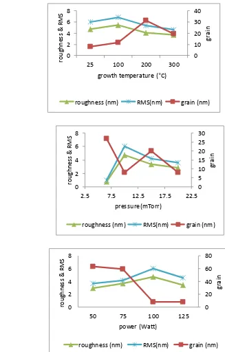
From the AFM test, the roughness, RMS and grain size is obtained. Figure 5 below shows that by varying the growth temperature, argon gas pressure and RF power, the results are significantly different. Surface roughness and RMS show that results are almost same as function of growth temperature and RF power, but abruptly low at low argon gas pressure. Roughness and RMS plays as important role in determining the interaction between samples and environment in term of forming cracks and corrosion (Black and Kohser, 2013; Den Outer et al., 1995). These factors are considered for solar cell application as crack and corrosion will reduce the solar cell efficiency in long period. On the other hand, higher roughness may promote better adhesion.
a
b
c
d
a
b
c
d
a
d
0
Fig. 5: Surface roughness, RMS and grain size as function of (a) Growth temperature (b) Argon gas pressure
(c) RF power
Grain size:
The grain size can be seen higher at 200 °C, below 75 Watt and fluctuated as function of argon gas pressure in Fig. 5. The higher grain size leads to be low resistivity that explains the current flow of the molybdenum thin films (Gordillo et al., 2006). The resistivity is the most important factor to be considered where lowers resistivity produce higher efficiency for solar cell application.
Conclusion:
best optimized condition for molybdenum deposition is at 200 °C, 6.6 mTorr and 75 Watt. Moreover all this research results properties show that the films is compatible and can be integrated not only for solar cell application but with wide variety of MEMS/NEMS devices and energy harvesters.
ACKNOWLEDGEMENT
This work was financially supported by Ministry Of Higher Education (MOHE), Malaysia through Universiti Teknikal Malaysia Melaka (UTeM) under research grant PJP/2012/FKEKK(7B)/S01099.
REFERENCES
Assmann, L., J.C. Berne`de, A. Drici, C. Amory, E. Halgand and M. Morsli, 2005. Study of the Mo thin films and Mo/CIGS interface properties. Applied Surface Science, 246(1-3): 159-166.
Barrera, E., F. Gonzalez, E. Rodriguez and J. Alvarez-Ramirez, 2010. Correlation of optical properties with the fractal microstructure of black molybdenum coatings. Applied Surface Science, 256(6): 1756-1763.
Black, J.T. and R.A. Kohser, 2013. DeGarmo’s Materials and Processes in Manufacturing (9th). Wiley, pp:
223.
Davidse, P.D., 1967. Theory and practice of RF sputtering. Vacuum, 17(3): 139-145.
Den Outer, A., J.F. Kaashoek and H.R.G.K. Hack, 1995. Difficulties with using continuous fractal theory for discontinuity surfaces. International Journal of Rock Mechanics and Mining Sciences & Geomechanics Abstracts, 32(1): 3-9.
Esmaeili-Rad, M.R. and S. Salahuddin, 2013. High performance Molybdenum Disulfide Amorphous Silicon heterojunction photodetector. Science Report, 3(2345).
Faiz, A., S. Anis, M.I. Idzdihar, M.Y. Mawarni, 2013. PV-Mini Hydro-Diesel Hybrid System in a village. International Journal of Engineering & Computer Science, 13(2): 1-7.
Faiz, A., S. Anis, M.S. Muzalifah, M.I. Idzdihar, 2014. Low-cost electro deposition of cuprous oxide P-N homo-junction solar cell. Advanced Materials Research, 827: 38-43.
George, S.J., O.B. Drury, J. Fu, S. Friedrich, C.J. Doonan, G.N. George, J.M. White, C.G. Young and S.P. Cramer, 2009. Molybdenum X-ray absorption edges from 200 to 20,000eV: The benefits of soft X-ray spectroscopy for chemical speciation. Journal of Inorganic Biochemistry, 103(2): 157-167.
Gordillo, G., F. Mesa and C. Calderon, 2006. Electrical and Morphological of Low Resistivity Mo thin films prepared by magnetron sputtering. Brazilian Journal of Physics, 36 (3B): 982-985.
Green, M.A., 2000. Power to the People: Sunlight to Electricity Using Solar Cells. UNSW Press.
Green, M.A., K. Emery, Y. Hishikawa, W. Warta and E.D. Dunlop, 2013. Solar cell efficiency tables (version 41), Progress in Photovoltaics: Research and Applications, 21: 1-11.
Gross, L., F. Mohn, N. Moll, P. Liljeroth and G. Meyer, 2009. The chemical structure of a molecule resolved by Atomic Force Microscopy. Science, 325(5944): 1110-1114.
Hossain, M.I., P. Chelvanathan, M. Zaman and N. Amin, 2011. Prospects of Indium Sulphide as an alternative to cadmimum sulphide buffer layer in CIS based solar cells from numerical analysis. Chalcogenide Letters, 8(5): 315-324.
Khatri, H and S. Marsillac, 2008. The effect of deposition parameters on radiofrequency sputtered molybdenum thin films. Journal of Physics: Condensed Matter, 20(5): 1-5.
Kuo, S.Y., M.J. Jeng, L.B. Chang, W.T. Lin, S.C. Hu, Y.T. Lu and C.W. Wu, 2009. Optimization of growth parameters for improved adhesion and electricity of molybdenum films deposited by RF magnetron sputtering.
34th Photovoltaic Specialists Conference (PVSC), pp: 594-596.
Löhmann, M., F. Klabunde, J. Bläsing, P. Veit and T. Drüsedau, 1999. Structural investigations on ultrathin Mo layers in a-Si:H with emphasis on the island-continuous layer transition, Thin Solid Films, 342(1-2): 127-135.
Pethe, S.A., E. Takahashi, A. Kaul and N.G. Dhere, 2012. Effect of sputtering process parameters on film properties of molybdenum back contact. Solar Energy Materials and Solar Cells, 100: 1-5.
Scofield, J.H., A. Duda, D. Albin, B.L. Ballardb and P.K. Predeckib, 1995. Sputtered molybdenum bilayer back contact for copper indium diselenide-based polycrystalline thin-film solar cells. Thin Solid Films, 260(1): 26-31.
Singh, R.N., D.M. Brown, M.J. Kim and G.A. Smith, 1985. Study of molybdenum‐aluminum interdiffusion
kinetics and contact resistance for VLSI applications. Journal of Applied Physics, 58(12): 4598-4604.
Takahashi, E., A. Shirish, Pethe and N.G. Dhere, 2010. Correlation between preparation parameters and
properties of molybdenum back contact layer for CIGS thin film solar cell. 35th Photovoltaic Specialists