Design of Reconfigurable Defected Ground Structure
(DGS) for UWB Application
Z. Zakaria, N. A .Shairi, R. Sulaiman and W. Y. Sam
Department of Telecommunication Engineering, Faculty of Electronic and Computer Engineering, Universiti Teknikal Malaysia Melaka (UTeM),
Hang Tuah Jaya, 76100 Durian Tunggal, Melaka, Malaysia.
E-mail: [email protected],[email protected], [email protected], [email protected]
Abstract—This paper presents the design of reconfigurable defected ground structure (DGS) resonator that can be integrated with ultrawide-band (UWB) microwave filter to produce bandpass and bandstop response simultaneously. The reconfigurable DGS is designed based upon coplanar waveguide (CPW) technology to exhibit bandstop characteristic at 3.5 GHz and 5.5 GHz using FR-4 on a 1.6 mm dielectric substrate thick with dielectric constant ࢿ࢘= 4.6. The simulation performance
shows promising results that could be further validated during the experimental works. This topology of reconfigurable DGS is useful for applications when the undesired signals need to be removed such as in wideband systems.
Keywords-Defected Ground Structure (DGS); Coplanar Waveguide (CPW); Ultra-wideband (UWB)
I. INTRODUCTION
The increasing development of wireless applications introduces new requirements for transceiver architecture that feature excellent performance and enhanced integration density. Since 1998, photonic band gap (PBG) structures [1] and defected ground structures (DGS) [2] have attracted the interest of many researchers. The used of DGS technology into coplanar waveguide transmission lines (CPW-TL) [3] compared to conventional transmission lines have many advantages such as to allow a simple reconfiguration as well as it is a very compact solution [4-7]. Furthermore, high performance, compact size and low cost often meet the stringent requirements of modern microwave communication systems.
In 2002, the Federal Communication Commission (FCC) authorized the frequency band from 3.1 GHz to 6.1 GHz for commercial applications [8]. Since then, there have been considerable research efforts put into ultra-wideband (UWB) radio technology worldwide. The UWB frequency band of 3.1 GHz to 10.6 GHz are interfering with the wireless local network signals such as WiMAX frequency at 3.5 GHz [9], and the WLAN systems operate in the 5.0 GHz frequency bands, e.g., 5.15 to 5.35 (IEEE 802.11a lower bands) and 5.725 to 5.825 GHz (IEEE 802.11a upper bands). Hence, a compact microwave bandpass filter working in the UWB system requires a design of reconfigurable bandstop filter in order to avoid being interfered by the undesired signals such as the WLAN radio.
In this paper, the design of reconfigurable defected ground structure (DGS) using coplanar waveguide (CPW) technology based on the study investigated in is presented.
II. DESIGN OF DGS
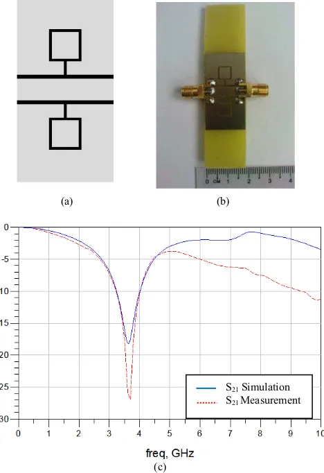
The design of the DGS is realized using coplanar waveguide (CPW). The procedures of realizing the structure can be found in [10] and [11]. Fig. 1 shows the layout for the dumbbell-shaped DGS resonator. It consists of a single square resonator whose pattern is etched in the ground plane of the CPW with a slot width, c.
Figure 1. Schematic diagram of DGS (half symmetrical view)
This structure is designed using FR4 substrate with dielectric constant, ߝr = 4.6, dielectric thickness, h = 1.6 mm, copper thickness = 0.035 mm, and loss tangent 0.019. CPW parameters are G/W/G = 0.715/4/0.715 mm in order to attain
50 Ω of input line impedance. The dimensions of A, B, C and D can be determined depending on resonant frequency and can be calculated according to the literature in [4].
A. Design of DGS at 3.5 GHz
Fig. 2 (a) shows the geometrical layout for the DGS to resonate at 3.5 GHz. The design is based on a single square resonator and constructed using Momentum Advanced Design System (ADS). The dimensions of the structure: A = 7 mm, B = 7 mm, C = 0.5 mm and D = 1 mm. The structure produces a single transmission zero at 3.5 GHz. The photograph of the fabricated DGS is shown in Fig. 2 (b), whilst the simulated and measured responses are shown in Fig. 2 (c). It can be observed that the insertion loss of -18 dB and a -10 dB bandwidth of 0.65 GHz are obtained particularly in the stopband. The
Top-layer (copper)
Square resonator
2012 IEEE Asia-Pacific Conference on Applied Electromagnetics (APACE 2012), December 11 - 13, 2012, Melaka, Malaysia
experimental result is in good agreement with the simulated response.
(a) (b)
(c)
Figure 2. (a) Layout of the DGS. (b) Fabricated DGS resonator. (c) Electromagnetic (EM) and measured S-Parameters (S21) results.
B. Design of DGS at 6.2 GHz
Fig. 3 (a) shows the geometrical layout for the DGS resonator and constructed using Momentum Advanced Design System (ADS). The dimensions of the structure: A = 4.14 mm, B = 4.14 mm, C = 0.5 mm and D = 1 mm. The structure produces a single transmission zero at 6.2 GHz. The photograph of the fabricated DGS is shown in Fig. 3 (b), whilst the simulated and measured responses are shown in Fig. 3 (c). It can be observed that the simulated return loss better than -15 dB and a -10 dB bandwidth of 0.97 GHz are obtained in the stopband. However, there is nevertheless a slight difference between measured and simulated response, which is due to the variations in manufacturing tolerance, thus producing imperfection in terms of physical dimensions differentiate between upper and lower square resonator.
(a) (b)
(c)
Figure 3. (a) Layout of the DGS. (b) Fabricated DGS3 resonator. (c) Electromagnetic (EM) and measured S-Parameters (S21) results.
III. DESIGN OF RECONFIGURABLE DGSTO PRODUCE TWO TRANSMISSION ZEROS
When a PIN diode is introduced at the square resonator (as shown in Fig. 4 (a), physical dimensions of the structure: A = 8.14 mm, B = 4.14 mm, C = 0.5 mm and D = 1 mm), the structure produce two transmission zeros and in this case approximately at 3.5 GHz and 5.5 GHz. This has due to the square structure a short bridge (when PIN diodes are ON) along its path causing the whole structure to separate into two basic structures, where each portion forms a ఒ
ସ resonator that
is terminated by a short circuit [4]. Thus, each resonator produces a single transmission zero at the corresponding frequencies as shown in Fig. 4 (b). Two transmission zeros at 3.45 GHz and 5.55 GHz with insertion loss better than -17 dB and – 13 dB have been obtained during the EM simulation. The -10 dB bandwidths of 0.45 GHz and 0.7 GHz have also been obtained, respectively. However, if the actual PIN diodes are used, the two transmission zeros will shifted to lower frequency due to the existence of series parasitic inductance in the PIN diodes during the ON state.
S21 Simulation S21 Measurement S21 Simulation
S21 Measurement
2012 IEEE Asia-Pacific Conference on Applied Electromagnetics (APACE 2012), December 11 - 13, 2012, Melaka, Malaysia
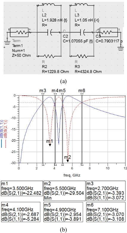
The structure can also be represented by the two parallel RLC resonators (shown in Fig. 5 (a)) and the circuit diagram response as shown in Fig. 5 (b) respectively. Two transmission zeros at 3.5 GHz and 5.5 GHz have obtained during the ideal circuit simulation. The -10 dB bandwidths of 0.5 GHz and 0.55 GHz have also been obtained, respectively.
The EM simulation performance of the reconfigurable DGS (with PIN diode) shows promising results and it is recommended to further verify during the experimental works in a laboratory.
(a)
(b)
Figure 4. (a) Layout of the DGS. (b) Electromagnetic (EM) S-Parameters (S21) results.
(a)
(b)
Figure 5. (a) Equivalent circuit of the DGS, and (b) Circuit simulation results.
IV. CONCLUSION
In this paper, the designs of defected ground structure (DGS) resonator based upon coplanar waveguide (CPW) technology have been presented. This involves the design of two DGS (without PIN diode) to produce a single transmission zero at 3.5 GHz and 6.2 GHz respectively. The simulated and measured results show the structures exhibit good performance particularly in the stop-band. The study has been further explored by simulating the reconfigurable DGS by introducing a PIN diode at the square resonator. The simulation performance of the structure shows excellent results by producing two transmission zeros and could be further verified during the experimental works. Therefore, these configurations of DGS could be integrated with any wideband microwave components such as UWB microwave filter to produce bandpass and bandstop characteristic in a single device simultaneously in order to reduce and minimize the overall physical volume and cost.
PIN diode location
PIN diode location
2012 IEEE Asia-Pacific Conference on Applied Electromagnetics (APACE 2012), December 11 - 13, 2012, Melaka, Malaysia
ACKNOWLEDGMENT
The authors would like to thank UTeM for sponsoring this work under the short term grant, UTeM, PJP/2012/FKEKK(11C)/S01015.
REFERENCES
[1] Radisic, V.; Qian, Y.; Coccioli, R.; Itoh, T.; , "Novel 2-D photonic bandgap structure for microstrip lines," Microwave and Guided Wave Letters, IEEE , vol.8, no.2, pp.69-71, Feb 1998.
[2] Chul-Soo Kim; Jun-Seok Park; Dal Ahn; Jae-Bong Lim; , "A novel 1-D periodic defected ground structure for planar circuits ," Microwave and Guided Wave Letters, IEEE , vol.10, no.4, pp.131-133, Apr 2000. [3] Jong-Sik Lim; Chul-Soo Kim; Young-Taek Lee; Dal Ahn; Sangwook
Nam; , "A spiral-shaped defected ground structure for coplanar waveguide," Microwave and Wireless Components Letters, IEEE , vol.12, no.9, pp.330-332, Sept. 2002.
[4] El-Shaarawy, H.B.; Coccetti, F.; Plana, R.; El-Said, M.; Hashish, E.A.; , "Novel Reconfigurable Defected Ground Structure Resonator on Coplanar Waveguide," Antennas and Propagation, IEEE Transactions on , vol.58, no.11, pp.3622-3628, Nov. 2010.
[5] El-Shaarawy, H.B.; Coccetti, F.; Plana, R.; El-Said, M.; Hashish, E.A.; , "Compact reconfigurable defected ground structure (DGS) based multiband bandpass filters on Coplanar Waveguide technology,"
Microwave Conference, 2009. APMC 2009. Asia Pacific , vol., no., pp.2022-2025, 7-10 Dec. 2009.
[6] El-Shaarawy, H.B.; Coccetti, F.; Plana, R.; , "A novel compact reconfigurable defected ground structure resonator on coplanar waveguide technology for filter applications," Antennas and Propagation Society International Symposium (APSURSI), 2010 IEEE , vol., no., pp.1-4, 11-17 July 2010.
[7] Jun Wang; Huansheng Ning; Lingfeng Mao; , "A Compact Reconfigurable Bandstop Resonator Using Defected Ground Structure on Coplanar Waveguide," Antennas and Wireless Propagation Letters, IEEE , vol.11, no., pp.457-459, 2012.
[8] Guo-Min Yang; Jin, R.; Vittoria, C.; Harris, V.G.; Sun, N.X.; , "Small Ultra-Wideband (UWB) Bandpass Filter With Notched Band," Microwave and Wireless Components Letters, IEEE , vol.18, no.3, pp.176-178, March 2008.
[9] G. S. V. Radha Krishna Rao and G. Radhamani, "WiMAX A Wireless Technology Revolution," Auerbach Publications, pp. 83-139, 2008. [10] R. Garg, P. Bhartia, I. Bahl and A. Ittipiboon, "Microstrip Antenna
Design Handbook", 2nd Edition, Boston: Artech House, pp. 786-789, 2001.
[11] Janaswamy, R.; Schaubert, D.H.; , "Characteristic Impedance of a Wide Slotline on Low-Permittivity Substrates (Short Paper)," Microwave Theory and Techniques, IEEE Transactions on , vol.34, no.8, pp. 900- 902, Aug 1986.
2012 IEEE Asia-Pacific Conference on Applied Electromagnetics (APACE 2012), December 11 - 13, 2012, Melaka, Malaysia