i
Defected Ground Structure with Circle Dumbbell Shape as a Quarter Wavelength
TEE KOK PENG
This report is submitted partial fulfillment of the requirement for the award of Bachelor of Electronic Engineering (Industrial Electronics/ Telecommunication Electronics/
Computer Engineering/ Wireless Communication) With Honours
Faculty of Electronic and Computer Engineering Universiti Teknikal Malaysia Melaka (UTeM)
ii
mengaku membenarkan Laporan Projek Sarjana Muda ini disimpan di Perpustakaan dengan syarat- syarat kegunaan seperti berikut:
1. Laporan adalah hakmilik Universiti Teknikal Malaysia Melaka.
2. Perpustakaan dibenarkan membuat salinan untuk tujuan pengajian sahaja.
3. Perpustakaan dibenarkan membuat salinan laporan ini sebagai bahan pertukaran antara institusi pengajian tinggi.
4. Sila tandakan ( √ ) :
(Mengandungi maklumat yang berdarjah keselamatan atau SULIT*
TERHAD*
TIDAK TERHAD
________________________________ (TANDATANGAN PENULIS)
Alamat Tetap: TN 11 SIMPANG EMPAT 78000 ALOR GAJAH MELAKA.
Tarikh: 21 APRIL 2011
kepentingan Malaysia seperti yang termaktub di dalam AKTA RAHSIA RASMI 1972)
iii
“I hereby declare that this report is the result of my own except for quotes as cited in the references”
Signature : ………
Author : TEE KOK PENG
iv
“I hereby declare that i have read this report and in my opinion this report is sufficient in terms of the scope and quality for the award of Bachelor of Electronic Engineering (Industrial Electronics/ Telecommunication Electronics/Computer Engineering*) with
Honours”.
Signature : ………..
Supervisor Name : EN. NOOR AZWAN BIN SHAIRI
v
Especially for
My beloved mom and dad
My family
My supervisor
MR. NOOR AZWAN BIN SHAIRI
All beloved friends
vii
ABSTRAK
viii
ABSTRACT
vi
ACKNOWLEDGEMENT
x
2.0 LITERATURE REVIEW 4
2.1 Defected Ground Structure (DGS) 4
2.2 DGS Equivalent Circuit 7
2.3 Application of DGS 8
2.3.1 Delay lines 9
2.3.2 Antennas 10
2.4 DGS as a Quarter Wavelength 10
3.0 METHODOLOGY 11
3.1 Project Methodology 11
3.2 Advanced Design System (ADS) 14
xi
4.1 Simulation Setup 23
4.1.1 Equivalent Circuit 24
4.1.2 Equivalent circuit simulation 29
4.1.3DGS Layout and Momentum Simulation 31
4.1.3.1DGS Layout Design 31
4.1.3.2 Momentum Simulation 32
5.0 LAYOUT, SIMULATION AND MEASUREMENT RESULTS
40
5.1 DGS Equivalent circuit 40
5.2 DGS Layout Design 42
5.2.11st design approach 42
5.2.2 2nd design approach 45
5.2.3 3rd design approach 47
5.3 Measurement of the DGS 49
6.0 CONCLUSION AND RECOMMENDATION 53
6.1 Conclusion 53
xii
LIST OF FIGURES
Figure 2.1:
Isometric view of dumbbell shaped DGS 5Figure 2.2: Distribution of surface current on the Ground Plane of a unit cell
DGS 5
Figure 2.3: Truncated Structure according to distribution of current on surface of
ground plane 6
Figure 2.4: Several resonant structures that may be used 7
Figure 2.5: The LC and equivalent circuit 8
Figure 3.1: Methodology Flowchart 13
Figure 3.2: Advanced Design System 14
Figure 3.3: Advanced Design System 2008 software main 15
Figure 3.4: Example of a Network Analyzer 20
Figure 3.5: The Electronic Calibration (Ecal) Module 22
Figure 4.1: Main Window of ADS 24
Figure 4.2: ADS schematic Window 24
xiii
Figure 4.4(a):S-Parameter item in schematic window 25
Figure 4.5(b): Option of S-Parameter 26
Figure 4.18: S-Parameter momentum simulations 35
Figure 4.19: Momentum simulation setup 36
Figure 4.20: Layout look-like options 37
Figure 4.21: Layout look-like options 37
Figure 4.22: Component Library 38
Figure 4.23: Choosing the project saved in the component library 39
Figure 5.1: Equivalent LC circuit 41
Figure 5.2: Relationship between Inductance and center frequency 41
Figure 5.3:Relationship between Capacitor and center frequency 42
xiv
Figure 5.5(a): Smith Chart graph of first DGS design 44
Figure 5.5(b): Phase graph of second DGS design 44
Figure 5.6: Second DGS layouts design 45
Figure 5.7(a): Smith Chart graph of second DGS design 46
Figure 5.7(b): Phase graph of second DGS design 46
Figure 5.8: Third DGS layouts design 47
Figure 5.9(a): Smith Chart graph of third DGS design 48
Figure 5.9(b): Phase graph of third DGS design 48
Figure 5.10(a): DGS design on FR4 board 49
Figure 5.10(b): 1st DGS design on FR4 board after soldering process of the port 50 Figure 5.10(c): 2nd DGS design on FR4 board after soldering process of the port 50 Figure 5.11(a): Comparison of simulation result and measurement result of
first DGS design 51
Figure 5.11(b): Comparison of simulation result and measurement result of
xv
LIST OF TABLES
Table 4.1: Comparison of simulation result and measurement result for two
1
CHAPTER 1
INTRODUCTION
1.1 Background
2
efficient coupling to the line. This project will further investigate the capability of DGS with circle dumbbell shape as a quarter wavelength at 2.4 GHz band. This project will use simulation tool to design and simulate the DGS. Then the prototype of DGS will be realized on FR4 board.
1.2 Project Objective
The objective of this project is to investigate the capability of DGS with circle dumbbell shape as a quarter wavelength at 2.4 GHz band. Then, this project will focus on the design and simulation of the DGS and finally realize the prototype on FR4 board.
1.3 Problem Statement
3
1.4 Project Scope
i. Studies the knowledge involved in this project such as Smith Chart and parameter in the DGS such as Scatting-Parameter, L-C Ratio and coupling coefficient.
ii. Design the DGS as quarter wavelength in ADS software as an equivalent circuit and layout.
iii. Simulate and analyze the DGS as a quarter wavelengths in the equivalent circuit and EM simulation in ADS software.
iv. Fabricate the selected DGS layout on FR4 board.
4
CHAPTER 2
LITERATURE REVIEW
2.1 Defected Ground Structure (DGS)
5
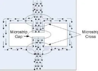
DGS is an etched periodic or non-periodic cascaded configuration defect in the ground of a planar transmission line such as microstrip, coplanar and conductor backed coplanar wave guided. DGS will disturb the shield current distribution in the ground plane cause of the defect in the ground.
This disturbance will change characteristics of a transmission line such as line capacitance and inductance [5]. In a word, any defect etched in the ground plane of the microstrip can give rise to increasing effective capacitance and inductance.
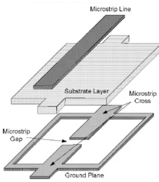
The isometric view of a conventional Defected Ground Structure is shown in Figure 2.1[2]; the surface current distribution on the ground plane resembles Figure 2.2. Taking this as the reference the ground plane of the DGS can be truncated as shown in Figure 2.3. The Frequency response of Figure 2.1 and Figure 2.3 being exactly the same, we would further the analysis of Fig. 3 in the light of different microstrip discontinuities.
Figure 2.1:Isometric view of dumbbell shaped DGS
6
Figure 2.3: Truncated Structure according to distribution of current on surface of ground plane
The DGS with Circle Dumbbell Shape has two circular areas on both sides. The area of circle is depending to the radius r, g x w gaps and a narrow connecting slot wide etched areas in backside metallic ground plane.
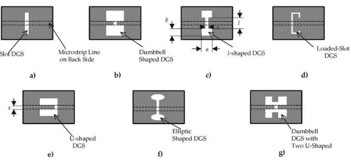
Figure 2.4 shows several resonant structures that may be used [9]. The basic
element of DGS is a resonant gap or slot in the ground surface (Figure 2.4a), placed
directly under the transmission line and aligned for efficient coupling to the line. The
dumbbell-shaped DGS (Figure 2.4b) includes two wide defected areas connected by a
narrow slot. The conventional dumbbell-shaped DGS has been modified into an
I-shaped DGS, as shown in Figure 2.4c. The frequency control of the I-I-shaped DGS is
accomplished by adjusting the length of the transverse slot and the dimensions a and b.
The stop-band characteristic of the DGS in Figure 2.4c depends on l, which is the
distance between two rectangular lattices. In the U-shaped structure of Figure 2.4e, the
loaded Q-factor increases as distance s decreases. Elliptic DGS cells are also obtained
by etching a slot that connects two elliptic DGS shapes in a microstrip ground plane
(Figure 2.4f). Figure 2.4g represents the DGS unit composed of two U-shaped slots
connected by a transverse slot. This DGS section can provide cutoff frequency and
7
Figure 2.4: Some resonant structures used for defected ground structure (DGS) applications
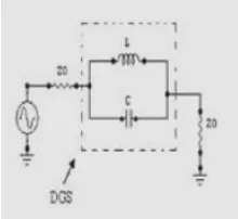
2.2 DGS Equivalent Circuit
The equivalent circuit of the DGS can be represented by a parallel LC resonant
circuit in series with the microstrip line. The transverse slot in the DGS increases the
effective capacitance, while the U-shaped slots attached to the transverse slot increase
the effective inductance of the microstrip line. This combination of DGS elements and
microstrip lines yields sharp resonances at microwave frequencies which can be
controlled by changing shape and size of the DGS circuitry. The shape and size of the
DGS slot controls both the fundamental resonant frequency and higher order resonances.
The size of the FR4 board area is also considered. To fulfill the different requirements,
a variety of DGS shapes have evolved over time, including dumbbell, periodic, circular,
spiral, L-, and H-shaped structures. There are three types of equivalent circuit, LC and
8
The parameters of equivalent circuit models of DGSs were also researched and utilized to design planar circuit easily [1].
Figure 2.5:LC equivalent circuit
2.3 Application of DGS
There are widely applications in active and passive devices useful for compact design. Since each DGS provides its own distinctive characteristics depending on the geometries, such circuit functionalities as filtering unwanted signals and tuning high-order harmonics can easily be accomplished by means of placing required DGS pattern, which correspond to the desired circuit operations without increasing circuit complexity[9].
2.3.1 Delay lines
9
mode transmission, but slows the even mode, which must propagate around the edges of the DGS “slot” [11].
2.3.2 Antennas
The filtering characteristics of DGS can be applied to antennas, reducing mutual coupling between antenna array elements, and reducing unwanted responses (similar to filters). This is the most common application of DGS for antennas, as it can reduce side lobes in phased array, improve the performance of couplers and power dividers, and reduce the response to out of band signals for both transmit and receive. An interesting application combines the slot antenna and phase shift behaviors of DGS. An array of DGS elements can be arranged on a flat surface and illuminated by a feed antenna, much like a parabolic reflector antenna. Each element re-radiates the exciting signal, but a phase shift can be built into the structure to correct for the distance of each element from the feed. The re-radiating elements introduce additional loss, but the convenience of a flat form factor is extremely attractive for transportable equipment or applications where a low-profile is essential.
2.3.3 Amplifier Design