UNIVERSITI TEKNIKAL MALAYSIA MELAKA
Design a Mini Depanelize Jig to Separate
PCBA’s
From Panel into Single Pieces.
This report submitted in accordance with requirement of the Universiti Teknikal Malaysia Melaka (UTeM) for the Bachelor Degree of Manufacturing Engineering
(Manufacturing Design) with Honours.
By
Mohd Zaidi bin Jakaria B050710183
UTeM Library (Pind.1/2007)
UNIVERSITI TEKNIKAL MALAYSIA MELAKA
BORANG PENGESAHAN STATUS LAPORAN PROJEK SARJANA MUDA
TAJUK: Design a Mini Depanelize Jig to Separate PCBA from Panel into Single Pieces
SESI PENGAJIAN: 2009/2010 Semester 2
Saya: Mohd Zaidi b. Jakaria
mengaku membenarkan Laporan PSM ini disimpan di Perpustakaan Universiti Teknikal Malaysia Melaka (UTeM) dengan syarat-syarat kegunaan seperti berikut:
1. Laporan PSM adalah hak milik Universiti Teknikal Malaysia Melaka dan punulis . 2. Perpustakaan Universiti Teknikal Malaysia Melaka dibenarkan membuat salinan
untuk tujuan pengajian sahaja.
3. Perpustakaan dibenarkan membuat salinan laporan PSM ini sebagai bahan pertukaran antara institusi pengajian tinggi. atau kepentingan Malaysia yang termaktub di dalam AKTA RAHSIA RASMI 1972)
(Mengandungi maklumat TERHAD yang telah ditentukan oleh organisasi/badan di mana penyelidikan dijalankan)
(TANDATANGAN PENULIS)
** Jika laporan PSM ini SULIT atau TERHAD, sila lampirkan surat daripada pihak berkuasa/organisasi berkenaan dengan menyatakan sekali sebab dan tempoh tesis ini perlu dikelaskan sebagai
DECLARATION
I hereby, declare this thesis entitle “Design a Mini Depanelize Jig to Separate the PCBA from Panel into Single Pieces” is the result of my own research except as sites
in the reference.
Signature :………..
Authors Name : Mohd Zaidi b. Jakaria
APPROVAL
This thesis submitted to the Senate of Universiti Teknikal Malaysia Melaka (UTeM) and has been accepted as partial fulfillment of the requirement for the degree of Bachelor of Manufacturing Engineering (Manufacturing Design). The members of supervisory committee are as follow:
……….
i
ABSTRACT
In order to optimize the productivity in PCBA manufacturing process, PCB’s are
design in panel form and have to be separated into single pieces before testing. This project is based on industrial problems at Cubic Electronics Sdn. Bhd. to cut the
ii
ABSTRAK
Dalam meningkatkan proses pengeluaran PCBA, PCB direkabentuk dalam bentuk panel dan perlu diasingkan/dipotong kepada satu satu bahagian litar. Projek ini berdasarkan masalah industri di Cubic Electronic Sdn. Bhd. untuk memotong litar daripada panel. Litar litar PCB ini di asing oleh lurah/alur V di atas dan bawah dan
perlu dipotong untuk digunakan. Teknik biasa yang digunakan adalah ‘punch’ dan
‘pizza cutters/circular rotating blade’ dan dilakukan secara manual oleh pekerja
iii
DEDICATION
For my mother, father and all my family and do not forget also to my friend and
iv
ACKNOWLEDGEMENT
v
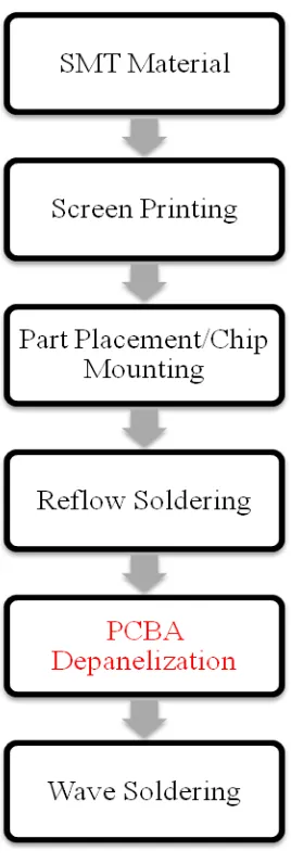
2.3.3 Part Placement/Chip mounting 10
2.3.4 Reflow Soldering 11
2.3.5 PCBA Depanelization 13
2.1.5.1 Current PCBA Depanelizer in Cubic Electronic Sdn. Bhd. 15
2.1.6 Wave Soldering 16
vi
3.1.1 Gantt Chart Clarification 25
3.2 Process Flow Chart 26
3.3 Process Flow 27
3.3.1 Data and Information Gathering 27
3.3.2 Identify Mechanism 28
3.3.3 Part Design 29
3.3.4 Material 32
3.3.5 Design Analysis 33
3.3.6 Design Simulation 35
4. RESULT AND ANALYSIS
4.0 Introduction 37
4.1 3D Modeling 37
4.2 Solidwork SimulationXpress 41
4.2.1 Existing Design 41
4.2.2 New Design 1 44
vii
5.1 Solidwork Simulationxpress Analysis 60
5.2 Time Study Analysis 62
5.3 Cost Analysis 63
6. CONCLUSION 65
7. RECOMMENDATION
7.0 Introductions 67
7.1 Suggestion and recommendation 67
REFERENCES 69
viii
LIST OF TABLE
Table 2.3.5: Depaneling Method 13
Table 2.3.5.1: Example of Circular Rotating Blade
(Current Cubic Electronic Method) 16
Table 3.3.1: PCB Panel Size 28
Table 3.3.4: FR-4 Halogen Free 33
Table 4.1: New Depanelize Jig Process 38
Table 4.2: Result on PCB Board Analysis 49
Table 4.3.1: Time Study for existing jig 52
ix
LIST OF FIGURES
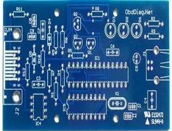
Figure 2.1: Printed Circuit Board 4
Figure 2.2: 18” x 24” (46mm x 61mm) panel example 5
Figure 2.3: V- Groove 6
Figure 2.4: SMT Flow Process 7
Figure 2.5: Solder Paste 8
Figure 2.6: solder paste screen or pattern 8
Figure 2.7: Printed Circuit Board (PCB) 8
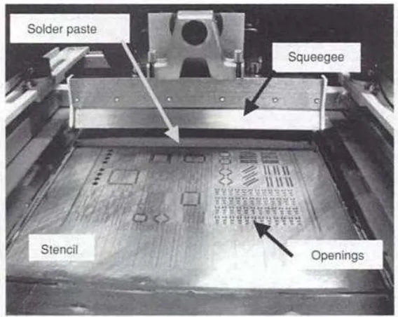
Figure 2.8: Stencil Printing 9
Figure 2.9: Printing Process Illustration 9
Figure 2.10: Surface Mount Technology (SMT) 10
Figure 2.11: CUBIC Electronic Chip/IC Mounting Machine 11 Figure 2.12: Reflow Oven Showing zones Creates the Profile 12 Figure 2.13: Temperature Profile for SMT Reflow Soldering 12
Figure 2.14: 3 Phase Diagram 13
Figure 2.15: Wave Soldering Process 17
Figure 2.11: Breakeven Chart 20
Figure 2.12: Jig and Fixture Standard Component 22
Figure 3.1: Gantt chart 24
Figure 3.2: Process Flow Chart 26
Figure 3.3: Surface Mount Technology (SMT) process 27
Figure 3.4: PCB Panel 28
Figure 3.5: Existing Jig 29
Figure 3.6: Solidwork toolbar 30
Figure 3.7: Some part design in 3D 30
Figure 3.8: Part Downloaded 31
Figure 3.9: Product after mating process 31
Figure 3.10: Material for Jig (solidwork library) 32
Figure 3.11: Material Selection 34
x
Figure 3.13: Solidwork Meshing processs 35
Figure 4.1: Mini Depanelize Jig 38
Figure 4.1: Force and Restrain applied (existing jig) 41
Figure 4.2: Stress on PCB (existing jig) 42
Figure 4.3: Safety Factor on PCB (existing jig) 43
Figure 4.4: displacement on PCB (existing jig) 43
Figure 4.5: Force and Restrain applied (New design 1) 44
Figure 4.6: Stress on PCB (New design 1) 45
Figure 4.7: Safety Factor on PCB (New design 1) 45
Figure 4.8: Displacement on PCB (New design 1) 46
Figure 4.9: Force and Restrain applied (New design 2) 47
Figure 4.10: Stress on PCB (New design 2) 48
Figure 4.11: Safety factor on PCB (New design 2) 48
Figure 4.12: Displacement on PCB (New design 2) 49
Figure 4.13: Flex Crack 50
Figure 4.14: Stress on Chip (existing jig) 51
Figure 4.15: Stress on Chip (New Design 2) 51
Figure 4.16: PCB Panel Cutting Line 52
Figure 5.1: Comparison Maximum Stress 61
Figure 5.2: Safety Factor & Displacement for 3 Designs 62
Figure 5.3: Output 63
Figure 5.4: Cost per part ` 64
xi
LIST OF ABBREVIATIONS
PCB Printed Circuit Board SMT Surface Mount Technology ICT In Circuit Test
PCBA Printed Circuit Board Assembly CAD Computer Aided Design
SMD Surface Mount Device
IR Infrared
1
CHAPTER 1
INTRODUCTION
1.1 Problem Background
Depanelization is one important process in high volume electronic assembly production i.e. PCBA printed circuit board assembly. In order to increase the output of printed circuit board (PCB) manufacturing and surface mount (SMT) lines,
(Surface-mount technology (SMT) is a method for constructing electronic circuits in
which the components, are mounted directly onto the surface of printed circuit
boards) PCB are often designed so that they consist of many smaller PCBs that will
be used in the final product. This PCB cluster is called panel or multi block. The
large panel is broken up or “depaneled” as a certain step in the process. The
depaneling process may happen right after SMT process, after in circuit test (ICT), after soldering of through hole element or even right before the final case-up of the assembly depending on the product or process.
There are few depaneling cutting techniques that have currently been used in industry nowadays. The techniques have been used are:
a) Hand break
b) V-cut / Pizza cutter (The use of a pizza cutter to avoid the dislodging of loose
toppings through the back-and-forth motion of the blade typical of a knife.)
2
1.2 Problem Statement
This project is based on industrial problems at Cubic Electronics Sdn. Bhd. to cut the printed circuit board. The PCB comes in a panel form contains from double up to 100 pieces of single PCB’s in one panel. The PCBs are separated by V-groove at top and bottom from one end to another and needs to be cuts in order to use them. The current technique is by using punch and pizza cutters and manually done by operators using jig or depanelize machine respectively. From the observations made at the company, the technique takes longer cycle time and difficult to handle for large panels. Although there is an automatic PCB cutter available in the market, the machine is far too expensive compared to the current machine. The current depaneling machines have their own advantages and disadvantages.
Advantages of current depaneling machine
1. Lower cost – low cost because lower money is invested to buy the machine
Disadvantages of current depaneling machine
1. Low productivity – less of outputs with longer cycle time need to operate the machine manually.
3
1.3 Objectives
The objectives of this study are to design a new PCB cutter machine which: 1. Design a PCB Depanelizing Jig
2. To reduce stress to PCB and chip during cutting process to reduce the reject part.
3. Cost effective – in term of overall performance of the machine and process for examples, reduce reject and cycle time.
4. Easy to handle – The operator easily can handle the machine without specific skills.
5. Improve the Productivity – use method and part that can improve the productivity of the output.
1.4 Scope of Project
In this project, several tools and equipment will be used in order to fulfil the objectives that have been stated. The scopes of this project are as follows:
1. PCB panel used is standard panel 18”x 24” (457mm x 610mm).
4
CHAPTER 2
LITERATURE RIVIEW
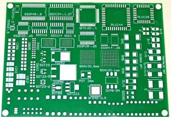
2.0 Printed Circuit Board (PCB)
In 1950’s electronic companies started using Printed Circuit Board (PCB) to reduce
cost and errors. A simple PCB contains an insulating substrate (the board) which made of phenolic (a material made from paper and resin), fibreglass or ceramic. Then a thin layer of copper printed/placed on the board in a particular pattern to connect all the components mounted to the board. (Al Williams, 2004)
5
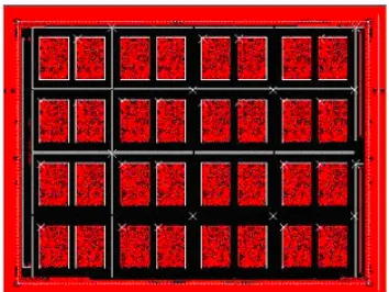
2.1 Panelization
Panelization is required for all SMT boards and smaller boards (whether through-hole or SMT) to increase processing efficiencies. There are some considerations
when deciding to panelize or not. From an assembler’s perspective, panels are
desirable and sometimes necessary to provide the tooling holes and PCB edge
clearance requirements. The PCB manufacturer’s material utilization and cost of an
electrical test fixture should also be considered, which the main priority is often. (Tommy Ewing, 2007. Sibex Electronic)
The following are some considerations for circuits intended for panelization.
1. If components overhang the edge of the PCB, adequate space between circuits to allow all components to be installed on the panelized PCBs is necessary. The layout may allow for component clearance on the adjacent PCB so that material usage is not sacrificed.
2. Panels can be either scored or routed or a combination of each depending on the
application. For routed PCB’s the breakaway tabs should be drilled for inside breakaway. Copper Trace or plane clearance at the location of the breakaway tabs
should be at least 0.10” from the PCB edge. For V-Score, see below guideline. 3. Component weight and panel size should be considered to reduce the possibility
of warpage and/or breakage. Panels that are wave soldered (i.e. Through Hole Components) will tend to sag in the center when subjected to preheat and reflow temperatures.
6
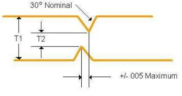
2.2 V-Groove
Figure 2.3: V- Groove
(Sanmina-SCI Company, http://www.Sanmina-SCI.com Copyright 2001 – 2007
Sanmina-SCI Corporation)
Minimum / maximum panel thickness (T1): 0.020” / 0.080” (0.5mm/2mm).
Maximum score distance: 25”.
Standard web thickness tolerance: +/- 0.005” (0.1mm). Preferred score angle: 30 +/- 2 degrees.
The standard/maximum web thickness (T2 in “Scoring diagram” figure): 0.012”/0.020” (0.3mm/0.5mm).
Traces should be ≥ 0.040” away from the score line center on all outer and inner layers.
Score line width should be 1.15 times the depth.
One score test coupon per score line should be included in the net list; these
7
2.3 Surface Mount Technology (SMT)
Surface mounts technology (SMT) which component leads are attached directly on the surface of the board. The component that suitable with this technology called surface mount device (SMD). (Clive Maxfield, 2002).
In surface mount technology, the traditional component lead through is replaced with solder paste to hold the component on the surface of the PCB. A solder paste
template is made that’s allowing the placement of the components at required area. Then all the required components is placed manually or usually automatically placed onto the solder paste. A baking process allows the solder paste liquefies and the components remain soldered to the PCB. (David A. Madsen 2001 Ed. 3)
8
2.3.1 SMT Tool/Material
The main raw material for screen printing is solder paste and the tool used are solder paste screen or pattern, solder paste and PCB.
Figure 2.5: Solder Paste
Figure 2.6: solder paste screen or pattern
9
2.3.2 Screen Printing
The most commonly used solder paste disposition is stencil printing although the other technology also is being use like dispensing, pin-transferring and roller coating. A stencil usually made from metal foil with a pattern similar to footprint of PCB where deposition of solder paste desired. The solder paste will be deposited onto the stencil and will be wiped with squeegee across the stencil. The stencil then will be detached from the surface of the PCB with solder paste on top of the corresponding pads. The printing process normally being used because of the higher speed, higher through-put, better patterns registration and better solder paste volume control. (Ning-Cheng Lee, 2002)
Figure 2.8: Stencil Printing