i
DESIGN AND CHARACTERIZATION OF VERTICAL MOSFET
NUR ASIMA BINTI MOHAMMAD NASIR
This Report Is Submitted In Partial Fulfillment of Requirements for the Bachelor Degree of Electronic Engineering (Computer Engineering)
Faculty of Electronics and Computer Engineering Universiti Teknikal Malaysia Melaka
ii
UNIVERSTI TEKNIKAL MALAYSIA MELAKA
FAKULTI KEJURUTERAAN ELEKTRONIK DAN KEJURUTERAAN KOMPUTER
BORANG PENGESAHAN STATUS LAPORAN PROJEK SARJANA MUDA II
Tajuk Projek : ………..…… Sesi
Pengajian : 1 1 / 1 2
Saya ……….. (HURUF BESAR)
mengaku membenarkan Laporan Projek Sarjana Muda ini disimpan di Perpustakaan dengan syarat-syarat kegunaan seperti berikut:
1. Laporan adalah hakmilik Universiti Teknikal Malaysia Melaka.
2. Perpustakaan dibenarkan membuat salinan untuk tujuan pengajian sahaja.
3. Perpustakaan dibenarkan membuat salinan laporan ini sebagai bahan pertukaran antara institusi pengajian tinggi.
4. Sila tandakan ( √ ) :
SULIT* *(Mengandungi maklumat yang berdarjah keselamatan atau kepentingan Malaysia seperti yang termaktub di dalam AKTA RAHSIA RASMI 1972)
TERHAD** **(Mengandungi maklumat terhad yang telah ditentukan oleh organisasi/badan di mana penyelidikan dijalankan)
TIDAK TERHAD
Disahkan oleh:
____________________________________ _____________________________________ (TANDATANGAN PENULIS) (COP DAN TANDATANGAN PENYELIA)
Tarikh: ………... Tarikh: ……….
DESIGN AND CHARACTERIZATION OF VERTICALMOSFET
NUR ASIMA BINTI MOHAMMAD NASIR
15th JUNE 2012
iii
“I declare that this thesis is the result of my own work except for quotes as cited in the references.”
Signature : ……….
iv
“I declare that I have been reading this thesis in view of our work is sufficient from the scope and quality for the award of Bachelor of Electronic Engineering (Computer
Engineering).”
Signature : ………
v
Dedicated to my beloved family To my father and mother To my respected lecturer/supervisor
And to all my friends
vi
ACKNOWLEDGEMENT
Firstly, the author would like to express utmost gratitude to the project supervisor, Mr. Zul Atfyi Fauzan bin Mohammed Napiah for his guidance and supervision for the project. The motivations and advices that he gave have helped her to overcome the complexities and the challenges that were posed by the project. The comments on the project throughout the whole progress of final year project have also helped the author to set clear and right path to achieve the goal set.
Next, the author would like to extent the appreciation for the support offered by parents and family in inspiring her to pursue in this study. The support and encouragement showered has made her more motivated while facing the problems in the project. Therefore, the author hopes the completion of the study will bring honors and contribution to the family.
vii
ABSTRACT
Vertical MOSFET is a device structure that considered overcoming the Short Channel Effects (SCEs) in nanometer scale device structure. In this research, the comparison between Drain-On-Top (DOT) and Source-On-Top (SOT) of Double Gate Vertical MOSFET were developed by using the SILVACO TCAD tools for several channel length (Lg) of 50, 70, 90, 130, and 180 nm respectively. The
performance of the Double Gate Vertical MOSFET was analyzed by using process and device simulation which are DevEdit, ATHENA and ATLAS tools respectively. The electrical characteristics for proposed devices have been analyzed based on different channel length and the results are as shown in the I-V curve. The physical parameters extracted from the I-V curve are the threshold voltage (VT), leakage
current (IOFF), active current (ION), Drain Induced Barrier Lowering (DIBL) and
viii
ABSTRAK
MOSFET Menegak adalah satu struktur peranti elektronik yang dipertimbangkan untuk mengatasi Kesan Saluran Pendek (SCEs) dalam struktur peranti berskala nanometer. Dalam kajian ini, perbandingan antara Saliran-Di-Atas (DOT) dan Sumber-Di-Atas (SOT) bagi MOSFET Menegak Get Duaan dilakukan dengan menggunakan perisian SILVACO TCAD untuk beberapa panjang saluran (Lg) iaitu 50, 70, 90, 130, dan 180 nm masing-masing. Prestasi MOSFET Menegak
Get Duaan telah dianalisa dengan menggunakan simulasi proses dan peranti iaitu DevEdit, ATHENA dan ATLAS masing-masing. Ciri-ciri elektrikal untuk peranti yang diusulkan telah dikaji berdasarkan panjang saluran yang berbeza dan hasil kajian adalah seperti yang ditunjukkan di dalam graf arus-voltan. Parameter fizikal yang diekstrak dari graf arus-voltan ambang (VT), arus bocor (IOFF), arus aktif (ION),
Drain Induced Barrier Lowering (DIBL) dan ayunan separa ambang. Daripada
ix
TABLE OF CONTENT
CHAPTER TITLE PAGE
PROJECT TITLE i
STATUS CONFIRMATION REPORT FORM ii
AUTHOR’S DECLARATION iii
SUPERVISOR’S DECLARATION iv
DEDICATION v
ACKNOWLEDGMENT vi
ABSTRACT vii
ABSTRAK viii
TABLE OF CONTENT ix
LIST OF TABLES xii
LIST OF FIGURES xiii
LIST OF ABBREVIATIONS xvi
LIST OF APPENDIX xvii
1 INTRODUCTION
1.1 BACKGROUND 1
1.2 PROBLEM STATEMENT 2
1.3 OBJECTIVES 3
1.4 SCOPE OF PROJECT 3
x
1.4.2 DevEdit 4
1.4.3 ATHENA 4
1.4.4 ATLAS 4
1.5 METHODOLOGY 5
1.6 PROJECT STRUCTURE OVERVIEW 6
2 LITERATURE REVIEW
2.1 PLANAR MOSFET 7
2.2 VERTICAL MOSFET 9
2.3 DOUBLE GATE VERTICAL MOSFET 10
2.4 SHORT CHANNEL EFFECTS (SCEs) 12
2.4.1 Threshold Voltage (VT) 12
2.4.2 Leakage Current (IOFF) 13
2.4.3 Active Current (ION) 14
2.4.4 Drain Induced Barrier Lowering (DIBL) 14
2.4.5 Sub-threshold Swing 15
3 METHODOLOGY
3.1 SUMMARY OF PROJECT FLOWS 16
3.2 INTRODUCTION TO TCAD TOOLS 18
3.2.1 SILVACO TCAD Tools 19
3.3 CREATING DOUBLE GATE VERTICAL
MOSFET STRUCTURE USING DEVEDIT 20
3.4 CREATING DOUBLE GATE VERTICAL
MOSFET STRUCTURE USING ATHENA 41
xi
4 RESULT AND DISCUSSIONS
4.1 DOUBLE GATE VERTICAL MOSFET
STRUCTURE BY USING DEVEDIT 56
4.1.1 Comparison of Drain-On-Top (DOT)
structure for various channel length 64 4.1.2 Comparison of Drain-On-Top (DOT) and
Source-On-Top (SOT) structure 67
5 CONCLUSION AND RECOMMENDATIONS
5.1 CONCLUSIONS 70
5.2 RECOMMENDATIONS 71
REFERENCES 72
APPENDIX A 74
APPENDIX B 76
xii
LIST OF TABLES
NO. TITLE PAGE
4.1 The threshold voltage of DOT structure for various channel
length 65
xiii
LIST OF FIGURES
NO. TITLE PAGE
1.1 Flow Chart of the Project 6
2.1 Planar MOSFET 8
2.2 Vertical MOSFET 9
2.3 Drain-On-Top Double Gate Vertical MOSFET 10
2.4 Source-On-Top Double Gate Vertical MOSFET 11
2.5 ID – VG curve 13
2.6 IOFF versus Lg curve 13
2.7 Output characteristic, Log ID – VG curve for DIBL 14
2.8 Output characteristic, Log ID – VG curve for sub-threshold
swing 15
3.1 Methodology of the Project 18
3.2 Resize the Work Area 20
3.3 Resized Area 21
3.4 Drawing the Base Region 22
3.5 Selecting “Set Base Impurity” 23
3.6 The Silicon Region 23
3.7 Drawing the Silicon Oxide Region 24
xiv
3.9 Adding Source Electrode 26
3.10 Setting of Doping Type of the Source 27
3.11 Source Electrode Region 27
3.12 Adding Drain Electrode 28
3.13 Setting Doping Type of the Drain 29
3.14 Drain Electrode Region 29
3.15 Substrate Electrode Panel 30
3.16 Adding Gate Electrode 31
3.17 Setting Doping Type of the Gate 32
3.18 The Polysilicon Gate Region 32
3.19 Add Impurity Panel for Source 33
3.20 User Added Impurity 34
3.21 Add Impurity Panel for Drain 35
3.22 User Added Impurity 36
3.23 Net Doping Example 37
3.24 Mesh Example 38
3.25 Double Gate Vertical MOSFET Structure 39
3.26 The Double Gate Vertical Structure with Mesh 40 3.27 The Double Gate Vertical Structure with Net Doping 40 3.28 The Double Gate Vertical Structure with both Mesh and Net
Doping 41
3.29 Creating Non-Uniform Grid in 0.39µm by 0.67µm Simulation
Area 42
3.30 Initial Triangular Grid 43
3.31 Codes for Etching 43
3.32 Silicon Pillar for Vertical MOSFET 44
3.33 Codes for gate oxidation and threshold voltage adjust implant 44 3.34 Contour Plot of the Boron doping profile after Ion
Implantation 45
3.35 Codes to Deposit the Polysilicon 45
xv
Polysilicon
3.38 Net Doping contour plot after Polysilicon implantation step 47 3.39 Codes for spacer oxide deposition and source/drain
implantation 48
3.40 Source/drain implantation 48
3.41 Codes for handling the metallization part 49
3.42 Half of the Double Gate Vertical MOSFET 50
3.43 Codes for mirror the structure and declare the electrodes 50 3.44 Full structure of DOT Double Gate Vertical MOSFET 51 3.45 Codes to load the .str file from DevEdit or ATHENA 52
3.46 Code for the recombination model 52
3.47 Codes for specifying the contact characteristics and interface
properties 53
3.48 Codes for the method statement 53
3.49 Codes to obtain ID – VG curve 54
3.50 ID – VG curve for VD = 0.1 V 54
3.51 Codes to obtain ID – VD curve 55
3.52 ID – VD curve 55
4.1 Drain-On-Top Double Gate Vertical MOSFET from DevEdit 57 4.2 Arsenic and Boron concentration for Drain-On-Top structure 58 4.3 Source-On-Top Double Gate Vertical MOSFET structure from
DevEdit 59
4.4 Arsenic and Boron concentration for Source-On-Top structure 60 4.5 The threshold voltage for 50nm DOT structure 61 4.6 The leakage current and active current for 50nm DOT structure 62
4.7 The DIBL for 50nm DOT structure 63
4.8 The sub-threshold swing for 50nm DOT structure 64 4.9 ID – VG curve for various channel length 64
4.10 Log ID – VG curve for various channel length 66
4.11 ID – VD curve for various channel length 67
4.12 ID – VG curve for DOT and SOT structure 68
xvi
LIST OF ABBREVIATIONS
AC - Alternating Current
DC - Direct Current
DIBL - Drain Induced Barrier Lowering
DOT - Drain-On-Top
FET - Field Effect Transistor
IC - Integrated Circuit
ID - Drain Current
IOFF - Leakage Current
ION - Active Current
Lg - Channel Length
MOSFET - Metal-Oxide Semiconductor Field Effect Transistor Nsub - Substrate Thickness
SCEs - Short Channel Effects
SOT - Source-On-Top
TCAD - Technology Computer Aided Design
tox - Oxide Thickness
VDS - Drain-Source Voltage
VGS - Gate-Source Voltage
VT - Threshold Voltage
xvii
LIST OF APPENDIX
NO. TITLE PAGE
A Example For Analyzing Drain-On-Top Structure From
DevEdit 74
B Example For Creating Drain-On-Top Structure Using
ATHENA 76
C Example For Analyzing Drain-On-Top Structure From
CHAPTER 1
INTRODUCTION
1.1 Background
2
It is impossible to be engaged in the semiconductor industry without encountering frequent references to Moore’s Law. In 1965, Gordon Moore, co-founder and chairman Emeritus of Intel Corporation, made the observation that the number of transistors per integrated circuit (IC) were growing at an exponential rate and predicted that this trend would continue. Since that time, the industry has an accomplished the exceptional feat of producing semiconductor devices with twice as many transistors as the prior generation every 18-24 months. Consumers and businesses alike have reaped tremendous benefits from the electronics technology, and semiconductors is the heart of it all [4].
Nowadays, research is focused on obtaining higher speeds, low power consumption, and low cost devices. Marketing leaders are very keen on inventing a new generation of MOSFET technologies to continue their dominating position [4]. Due to physical device fabrication limitations and short channel effects, the future of MOSFET relies on the evaluation of new techniques like Vertical MOSFET and Double Gate MOSFET.
1.2 Problem Statement
An integrated circuit (IC) is a minuscule electronic circuit that consists of active and passive components as well as interconnection. These components include transistor, diode, capacitor, and resistor. The IC is based mainly on the transistor. The transistor, a semiconductor device was developed as an alternative to the old vacuum tube.
3
almost all electronic equipment. The recent development of MOSFET has reached the progress that the channel length goes shorter into nanometer scale.
While the MOSFET undergoes scaling down of the size in order to improve integrated circuit performance such as speed, power consumption and packing density, a number of challenges need to be overcome.
1.3 Objectives
The objectives of this project are:
(i) To be familiarize with SILVACO TCAD tools.
(ii) To design and characterize the Vertical MOSFET (Metal-Oxide-Semiconductor Field Effect Transistor).
(iii) To compare the performance of Vertical MOSFET and other relevant device structure.
1.4 Scope of Project
4
1.4.1 Introduction to TCAD
TCAD stands for Technology Computer Aided Design, which is not that self-explanatory. What it really refers to is computer programs able to simulate either the workings of a semiconductor device (device simulation) or the fabrication process of a semiconductor device (process simulation). Often the result of a process simulation, which is called a “mesh” or “grid”, is fed into a device simulator to evaluate the performance or the behavior of the device that has been “virtually fabricated”. Simulations are very inexpensive and fast compared to actual prototype fabrication. They are also an excellent tool to understand semiconductor physics.
1.4.1 DevEdit
DevEdit can be used to either create a device from scratch or to re-mesh or edit an existing device. DevEdit creates standard SILVACO structures that are easily integrated into SILVACO 2D or 3D simulators and other support tools.
1.4.2 ATHENA
ATHENA provides a convenient platform for simulating processes used in semiconductor industry such as ion implantation, diffusion, oxidation, physical etching and deposition, lithography, stress formation and silicidation.
1.4.3 ATLAS
physics-5
based, easy to use, modular and extensible platform to analyze DC, AC and time domain responses for all semiconductor based technologies in 2 and 3 dimensions.
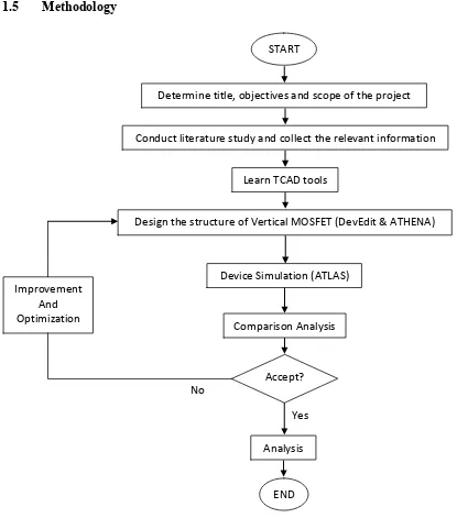
[image:22.595.111.526.185.656.2]1.5 Methodology
Figure 1.1: Flow Chart of the Project
No
Determine title, objectives and scope of the project
Conduct literature study and collect the relevant information
Design the structure of Vertical MOSFET (DevEdit & ATHENA) Learn TCAD tools
Accept?
Device Simulation (ATLAS)
Comparison Analysis
Analysis START
END Improvement
And Optimization
6
1.6 Project Structure Overview
This thesis consists of five chapters. The first chapter provides an introduction to this project. This includes the objectives and importance of this project. The second chapter contains theories and information about other relevant researchers conducted by research institutes and universities around the world.
The research activities and methods employed in this project will be discussed in detail in Chapter 3. This chapter shows the flow of this project from the very beginning of the data collection until the acceptable results. It also introduced the TCAD tools used in this project. Step by step explanations on the development of the Vertical MOSFET are provided for extra information and knowledge.
Chapter four will discuss about the result obtained from the process simulation using ATLAS tools. The data and results from the process are analyzed and discussed in this chapter. The effect of the tested parameters is discussed and opinions are brought forward in this chapter. Comparison between the Drain-On-Top (DOT) and Source-On-Top (SOT) structure are also discussed.
CHAPTER 2
LITERATURE REVIEW
This chapter provides an introduction to MOSFET inclusive of an overall view of the past and current technology revolving around it. Backgrounds of the planar MOSFET to the novel device of Double Gate Vertical MOSFET were illustrated in this chapter. The previous research paper that had been selected to be the key papers was also discussed in this chapter.