Dept. of Electrical Engineering, Diponegoro University, Semarang, Indonesia 50275
4
Dept. of Physics, Diponegoro University, Semarang, Indonesia 50275 *Corresponding author, e-mail: [email protected]
Abstract
Non-planar structures have been identified as promising structure for next device generation in the nanoelectronic era. However, the continuous device dimension scaling into nano regime eventually requires more sophisticated model due to the limitation of the existing models. A model for non-planar MOSFET structure was elaborated in this paper, especially for device with pillar structure, using analytical approach. The concern of channel shape and structure were discussed as well. The result shows the shift in subthreshold characteristic in the channel with recessed channel model. The charge sharing is suspected as one of the key parameter in the shift of performance in the recessed region.
Keywords: non-planar MOSFET, nanoscale, analytical model, surface potential, short channel effect
1. Introduction
The rapid development of MOSFET have shown a tremendous progress in downscaling the dimension and structure as well into nanoscale. The continuous scaling of the device dimension has now reached tens of nanometer size especially for the channel length of transistors. With the smaller device dimension, it is getting impossible to maintain the conventional bulk structure legacy, as shown by International Technology Roadmap for Semiconductor (ITRS) [1]. Several future devices with non-conventional structure have been proposed to overcome the conventional MOSFET structure limitations, as example in [2]-[8]. The non-planar MOSFET is expected to expand the Moore’s law. Several structures could shift the downsizing off the lithography and obtain self-aligned multi gate which is hard to produce with conventional one.
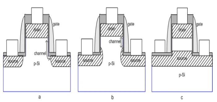
On the other hand, several fabrication methods produces various channel shapes, Some methods result in straight channel between source and drain, while some others create such a bending channel, a combination of vertical and recessed horizontal direction of current. For example, several geometries may be found in non-planar double gate MOSFET. Figure 1(a) reveals the recessed channel with L-shaped geometry due to the presence of corner that diverts the direction of current from drain to source. The second geometry, shown in Figure 1(b), offers the possibility of direct flux. This body-tied geometry have its channel connected to the substrate potential. The floating body channel (Figure 1(c)) reveals simple double gate structure but with its channel potential isolated electrically from the substrate.
channel, (b) body-tied channel, and (c) floating-body channel
Therefore, in order to explain the behaviour of channel with different shape and potential profile, it is important to derive the appropriate model. In addition, the continuous scaling of device requires applicable model in nanoscale. This paper elaborates the analytical model of non-planar MOSFET which employ the recessed channel geometry in the bottom part. The corner effect is elaborated extensively, with the help of approach that has been provided for conventional model [17]. In addition, the preceeding reports on this model have also been reported in [18]. This extended report provides more evaluation on the short channel effects which are crucial in the nano regime.
2. Analytical Model
The structure of recessed channel in non-planar MOSFET can be seen in Figure 2. This typical structure is an ideal form of the fabricated devices. The straight channel potential model is derived from Poisson equation using generic approach as noted in several references, e.g. [10],[19]-[22]:
, ,
(1)
Moreover, the presence of corner region in the bottom is arguably difficult to solve using two-dimensional Poisson equation in Cartesian system. Therefore, we divide the channel into two regions: first is the straight and latter is the corner region. We simplify the corner region as a quarter circle, an approach adopted from Zhang et al [17] for grooved gate in conventional MOSFET. However, Zhang’s model used trapezium-shape approach, while our model employs quarter-circle approach which is more realistic.
The uniformed depletion width is calculated using the following formula:
(2)
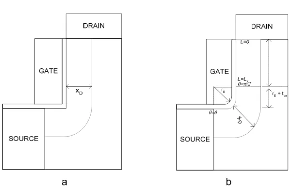
[image:2.595.124.475.73.239.2]Figure 2. The structure of recessed channel in vertical geometry (a), and its approach using two-region solution (b)
The potential of channel for each region is following the two dimensional second-order parabolic approach of graded channel approximation (GCA) that originally proposed by Young [24]. However, for corner area, the parabolic approximation is adopted to the cylindrical coordinate system as was used in [17]. The potential for both cartesian and polar coordinate systems are:
ψ , (3)
ψ , (4)
The notation “st” stands for “straight”, to differentiate with “cr” for “corner”. In solving the differential Poisson equation using general parabolic approach, several boundary conditions are set, which are applied to both regions (for polar coordinate, x and y should be replaced with and r, respectively):
The electric field in the silicon-oxide interface is according to Gauss’ law [23]:
(5)
(i) The potential at depletion layer is equal to the substrate potential, for body-tied channel to the Vsub :
, (6)
(ii) The electric field in the depletion layer is:
(7)
All parameters are put and later the potential equation is rewritten as:
, (8)
′′ (11)
Similarly for corner area, the surface potential of Eq. 9 is substituted into Poisson’s equation for polar coordinate [17]:
ψ ψ
(12)
which result in [17]
′′ (13)
It is noteworthy that Poisson equation of both regions as expressed in Eqs. 10 and 12 can be rearranged in the generic second-order differential equation formula [26] which has the common form of:
′′
λ , for straight (14)
′′ , for corner (15)
The respective boundary conditions for both regions can be defined as:
(i) ψ ,
(ii) ψ ,
(iii)
(iv) (16)
Threshold voltage VT is determined when the value of minimum surface potential is
twice the Fermi potential , . Thus, the location of the minimum potential along the surface in the channel obeys the expression:
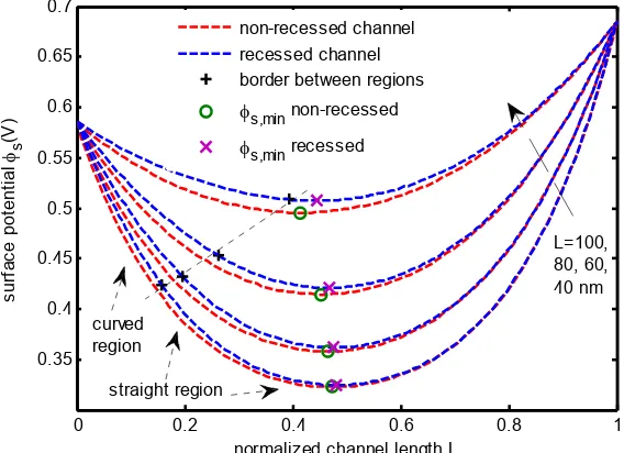
tied structure, the body of channel outside the depletion region is assumed to have the potential of substrate, . Meanwhile, Figure 4 shows the surface potential with the recessed channel is limited to around 15% of the total channel length L. It is notable that the minimum surface potential is located in the straight region for Lrec < 40% L.
[image:5.595.146.428.514.714.2]Figure 3. The surface potential for recessed and non-recessed channel. the length recessed part are constant (10 nm), Vds =0.1 V. tox = 3 nm, Vgs=0.1V
Figure 4. The surface potential as a function of normalized channel length, with the recessed region length are 15% of L. Vds =0.1 V. tox = 3 nm, Vgs=0.1V
0 0.2 0.4 0.6 0.8 1
0.35 0.4 0.45 0.5 0.55 0.6 0.65 0.7
normalized channel length L
s ur fa c e pot ent ial s (V ) non-recessed channel recessed channel border between regions
s,min non-recessed
s,min recessed
curved region straight region L=100, 80, 60, 40 nm
0 0.2 0.4 0.6 0.8 1
0.35 0.4 0.45 0.5 0.55 0.6 0.65 0.7
normalized channel length L
s u rf a c e pot ent ia
l
s
(V
)
non-recessed channel recessed channel border between regions
s,min non-recessed
s,min recessed
Figure 5. The threshold voltage due to short channel effect
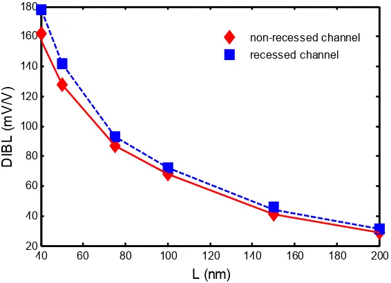
Figure 6. The drain-induced barrier lowering for recessed and non-recessed channel, at Vds=0.1
and 1.0 V
40 60 80 100 120 140 160 180 200
0.5 0.55 0.6 0.65 0.7 0.75
L (nm)
V T
(V
)
non-recessed channel recessed channel
40 60 80 100 120 140 160 180 200
20 40 60 80 100 120 140 160 180
L (nm)
D
IBL
(
m
V/
V
)
[image:6.595.151.434.508.713.2]4. Conclusion
The non-planar MOSFET structure with recessed channel has been modeled analytically using parabolic approach. Two distict region representing different channel shape were applied for the ease of model. The simulation based on the developed model shows the shift of threshold voltage due to the presence of the recessed part in the corner. In addition, the DIBL reveals the tendency of increasing in the lower channel length, as a manifestation of the short channel effect. While the straight channel offers lower threshold voltage, the higher DIBL is found for recessed channel. The result reveals the implication of the usage of pillar for non-planar structure, which requires more careful design in the future for threshold-sensitive application .
References
[1] ITRS. International Technology Roadmap for Semiconductors (ITRS). 2013. Available: http://www.itrs.net/reports.html
[2] T. Endoh, et al. Sub-10 nm Multi-Nano-Pillar Type Vertical MOSFET. IEICE Transactions on Electronics. 2010; E93-C: 557-562.
[3] A. Sugimura, et al. Proposal of Vertical-Channel Metal Oxide Semiconductor Field-Effect Transistor with Entirely Oxidized Silicon Beam Isolation. Japanese Journal of Applied Physics. 2009; 48. [4] MA. Riyadi, et al. Vertical Double Gate MOSFET For Nanoscale Device With Fully Depleted Feature.
AIP Conference Proceedings. 2009;1136: 248-252.
[5] J. Pan. The Gate-Controlled Diode, High-Frequency, and Quasi-Static C-V Techniques for Characterizing Advanced Vertical Trenched Power MOSFETs. IEEE Transactions on Electron Devices. 2009; 56: 1351-1354.
[6] M. Masahara, et al. Vertical Ultrathin-channel Multi-gate MOSFETs (MuGFETs): Technological Challenges and Future Developments. IEEJ Transactions on Electrical and Electronic Engineering. 2009; 4: 386-391.
[7] L. Tan, et al. The influence of junction depth on short channel effects in vertical sidewall MOSFETs. Solid-State Electronics. 2008; 52: 1002-1007.
[8] J. Moers. Turning the world vertical: MOSFETs with current flow perpendicular to the wafer surface. Applied Physics A: Materials Science & Processing. 2007; 87: 531-537.
[9] Y. Taur, et al. "A continuous, analytic drain-current model for DG MOSFETs. IEEE Electron Device Letters. 2004; 25: 107-109.
[10] Y. Taur. An analytical solution to a double-gate MOSFET with undoped body. IEEE Electron Device Letters. 2000; 21: 245-247.
[11] XP. Liang, Y. Taur. A 2-D analytical solution for SCEs in DG MOSFETs. IEEE Transactions on Electron Devices. 2004; 51: 1385-1391.
[12] J. He, et al. A continuous analytic channel potential solution to doped symmetric double-gate MOSFETs from the accumulation to the strong-inversion region. Chinese Physics B, 2011; 20. [13] K. Chandrasekaran, et al. Compact modeling of doped symmetric DG MOSFETs with regional
approach. in Workshop on Compact Modeling, NSTI-Nanotech, MA, USA. 2006: 792 - 795.
[14] D. Munteanu, et al. Compact model of the quantum short-channel threshold voltage in symmetric Double-Gate MOSFET. Molecular Simulation. 2005; 31: 831-837.
[15] S. Kolberg, TA. Fjeldly. 2D Modeling of nanoscale DG SOI MOSFETs in and near the subthreshold regime. Journal of Computational Electronics, 2006; 5: 217-222.
[16] B. Subrahmanyam, MJ. Kumar. Recessed source concept in nanoscale vertical surrounding gate (VSG) MOSFETs for controlling short-channel effects. Physica E-Low-Dimensional Systems & Nanostructures. 2009; 41: 671-676.
[25] X. Zhang, et al. An Analytical Model for Threshold Voltage of Grooved-Gate MOSFET's [in Chinese]. Chinese Journal of Semiconductors. 2004; 4: 441-445.
[26] E. Kreyszig. Advanced engineering mathematics, 9th ed. Wiley. 2006.
[27] B. Doris, et al. Extreme scaling with ultra-thin Si channel MOSFETs. Electron Devices Meeting,2002 IEDM'02. Digest. International. 2002: 267-270.